

Datasheet TV15C5V0K-B, TV15C5V0J-B, TV15C6V0K-B, TV15C6V0J-B, TV15C6V5K-B Datasheet (COMCHIP)
...Page 1
查询TV15C100J供应商
SMD Transient Voltage SuppressorSMD Transient Voltage Suppressor
TV15C5V0 Thru TV15C171
Working Peak Reverse Voltage: 5.0 - 170 Volts
Power Dissipation: 1500 Watts
Features
Ideal for surface mount applications
Easy pick and place
Plastic package has Underwriters Lab.
flammability classification 94V-0
Typical IR less than 1uA above 10V
Fast reponse time: typically less 1nS for
uni-direction, less than 5nS for bi-
directiona, from 0 V to BV min.
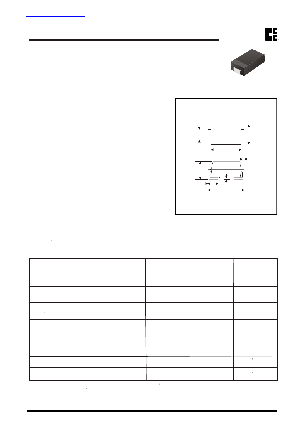
Mechanical data
Case: JEDEC DO-214AB molded plastic
Terminals: solderable per MIL-STD-750,
method 2026
Polarity: Cathode band denoted
Mounting position: Any
Approx. Weight:0.21 gram
0.124(3.15)
0.108(2.75)
0.050(1.27)
0.030(0.76)
COMCHIPCOMCHIP
www.comchip.com.tw
SMC/DO-214AB
0.280(7.11)
0.260(6.60)
0.103(2.62)
0.079(2.00)
Dimensions in inches and (millimeter)
0.320(8.13)
0.305(7.75)
0.245(6.22)
0.220(5.59)
0.012(0.31)
0.006(0.15)
0.008(0.20)
0.0203(0.10)
Maximum Ratings and Electrical Characterics
Rating at 25 C ambient temperature unless otherwise specified.
Single phase, half wave, 60Hz, resistive or inductive load.
For capacitive load, derate current by 20%
Characteristics
Peak Power Dissipation on 10/1000uS
Waveform (Note 1, Fig. 1)
Peak Pulse Current of on 10/1000uS
Waveform (Note 1, Fig. 3)
Steady State Power Dissipation at
TL=75 C (Note 2)
Peak Forfard Surge Current, 8.3mS Single
Half Sine-Wave Superimposed on Rated
Load, Uni-Directional Only (Note 3)
Maxinum Instantaneous Forward Voltage
at 100A for Uni-Directional only
(Note 3 & 4)
Operation Junction Temperature Range
Storage Temperature Range
Note: 1. Non-Repetitive Current Pulse, per Fig. 3 and Derated above TA=25 C, per Fig. 2.
2. Mounted on 8.0x8.0 mm . Copper Pads to Each Terminal.
3. Measured on 8.3 mS Single Half Sine-Wave or Equivalent Square Wave, Duty Cycle=4 Pulse per Minute Maximum.
4. VF=3.5V on TV15C5V0 thru TV15C900 Devices and VF=5.0V on TV15C101 thru TV15C171.
Symbol
PPPM
IPPM
PM(AV)
IFSM
VF
Tj
TSTG
Value
1500
See Table 1
5.0
200
3.5/5.0
-55 to +150
-55 to +150
Units
Watts
A
Watts
A
Volts
C
C
MDS0211016A
Page 1
Page 2
SMD Transient Voltage SuppressorSMD Transient Voltage Suppressor
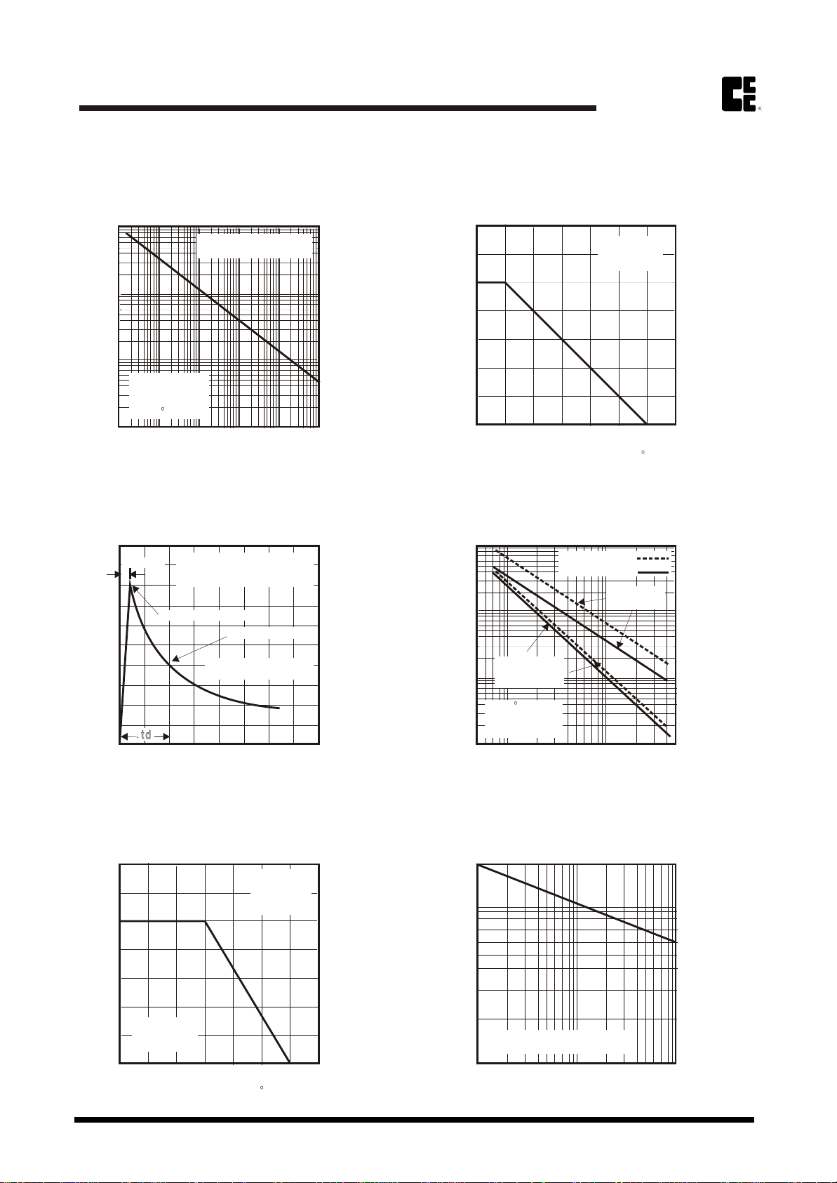
Rating and Characteristic Curves (TV15C5V0 Thru TV15C171)
COMCHIPCOMCHIP
www.comchip.com.tw
Fig. 1 - Reverse Characteristics
100
10
1.0
Non-Repetitive
Peak Pulse Power, PPPM (KW)
Pulse Waveform
Shown in Fig. 3
TA=25 C
0.1
0.1 1.0 10 100 1000 10000
Mounted on 8mmx8mm
Copper Pads
Pulse Width, td (uS)
Fig. 3 - Pulse Waveform
125
tr =10uS
100
75
50
25
Peak Pulse Current, IPPM ( %)
0
0 1.0 2.0 3.0 4.0
Pulse Width (td) is Defined
as the Point Where the peak
Current Decay to 50% of Ipp
Peak Value IPPM
Half Value Ipp/2
10/1000 uS Waveform
as Defined by R.E.A.
Time, t (mS)
Fig. 2 - Pulse Derating Curve
140
Mounted on
120
100
80
60
40
20
Peak pulse Power (Ppp) or Current (Ipp)
Derating in Percent (%)
0
0 25 50 75 100 125 150 175
Ambient Temperature,TA ( C)Ambient Temperature,TA ( C)
5mmx5mm
Copper pads
Fig. 4 - Typical Junction Capacitance
for Uni-Directional Devices
10,000
Uni-Directional
Bi-Directional
1,000
Measure at
100
Junction Capacitance, Cj (pF)
0
Standard-off
Voltage, Vwm
Tj=25 C
f=1.0MHz
Vsig=50mVp-p
5.0 10 100 500
Breakdown Voltage,VBR (Volts)
Measure at
Zero Bias
Fig. 5 - Steady State Power Derating Curve
7.0
6.0
5.0
4.0
3.0
2.0
Steady State Power Dissipation,
PM(AV), Watts
1.0
0
MDS0211016A
Mounted on
8mmx8mm
Copper pads
0 25 50 75 100 125 150 175
Leadt Temperature,TL ( C)
60Hz
Resistive or
Inductive
Load
Fig. 6 - Maxinum Non-Repetitive Peak
Forward Surge Current (Uni Directional Only)
200
100
50
20
Peak Forward Surge Current, IFSM (A)
8.3mS Single Half Sine-Wave
(JEDEC Method) Tj=Tjmax
10
1 10 100
Number of Cycle at 60Hz
Page 2
Page 3

SMD Transient Voltage SuppressorSMD Transient Voltage Suppressor
Part No. VRWM VBR Mi n VBR Ma x IT IFSM IR @VRWM
( V ) ( V ) ( V ) ( mA ) (A) @8.3mS ( V ) Ipp(A) ( uA ) UNI BI
TV15C5V0K(B) 5.00 6.40 7.55 10 100 9.6 156.2 800 GDD BDD
TV15C5V0J(B) 5.00 6.40 7.25 10 100 9.2 163.0 800 GDE BDE
TV15C6V0K(B) 6.00 6.67 8.45 10 100 11.4 131.6 800 GDF BDF
TV15C6V0J(B) 6.00 6.67 7.67 10 100 10.3 145.6 800 GDG BDG
TV15C6V5K(B) 6.50 7.22 9.14 10 100 12.3 122.0 500 GDH BDH
TV15C6V5J(B) 6.50 7.22 8.30 10 100 11.2 133.9 500 GDK BDK
TV15C7V0K(B) 7.00 7.78 9.86 1 100 13.3 112.8 200 GDL BDL
TV15C7V0J(B) 7.00 7.78 8.95 1 100 12.0 125.0 200 GDM BDM
TV15C7V5K(B) 7.50 8.33 10.67 1 100 14.3 104.9 100 GDN BDN
TV15C7V5J(B) 7.50 8.33 9.58 1 100 12.9 116.3 100 GDP BDP
TV15C8V0K(B) 8.00 8.89 11.30 1 100 15.0 100.0 50 GDQ BDQ
TV15C8V0J(B) 8.00 8.89 10.23 1 100 13.6 110.3 50 GDR BDR
TV15C8V5K(B) 8.50 9.44 11.9 1 100 15.9 94.3 10 GDS BDS
TV15C8V5J(B) 8.50 9.44 10.8 1 100 14.4 104.2 10 GDT BDT
TV15C9V0K(B) 9.00 10.00 12.6 1 100 16.9 88.7 5 GDU BDU
TV15C9V0J(B) 9.00 10.00 11.5 1 100 15.4 97.4 5 GDV BDV
TV15C100K(B) 10.00 11.10 14.1 1 100 18.8 79.8 5 GDW BDW
TV15C100J(B) 10.00 11.10 12.8 1 100 17.0 88.2 5 GDX BDX
TV15C110K(B) 11.00 12.20 15.4 1 100 20.1 74.6 5 GDY BDY
TV15C110J(B) 11.00 12.20 14.0 1 100 18.2 82.4 5 GDZ BDZ
TV15C120K(B) 12.00 13.30 16.9 1 100 22.0 68.2 5 GED BED
TV15C120J(B) 12.00 13.30 15.3 1 100 19.9 75.3 5 GEE BEE
TV15C130K(B) 13.00 14.40 18.2 1 100 23.8 63.0 5 GEF BEF
TV15C130J(B) 13.00 14.40 16.5 1 100 21.5 69.7 5 GEG BEG
TV15C140K(B) 14.00 15.60 19.8 1 100 25.8 58.1 5 GEH BEH
TV15C140J(B) 14.00 15.60 17.9 1 100 23.2 64.7 5 GEK BEK
TV15C150K(B) 15.00 16.70 21.1 1 100 26.9 55.8 5 GEL BEL
TV15C150J(B) 15.00 16.70 19.2 1 100 24.4 61.5 5 GEM BEM
TV15C160K(B) 16.00 17.80 22.6 1 100 28.8 52.1 5 GEN BEN
TV15C160J(B) 16.00 17.80 20.5 1 100 26.0 57.7 5 GEP BEP
TV15C170K(B) 17.00 18.90 23.9 1 100 30.5 49.2 5 GEQ BEQ
TV15C170J(B) 17.00 18.90 21.7 1 100 27.6 53.3 5 GER BER
TV15C180K(B) 18.00 20.00 25.3 1 100 32.2 46.6 5 GES BES
TV15C180J(B) 18.00 20.00 23.3 1 100 29.2 51.4 5 GET BET
TV15C200K(B) 20.00 22.20 28.1 1 100 35.8 41.9 5 GEU BEU
TV15C200J(B) 20.00 22.20 25.5 1 100 32.4 46.3 5 GEV BEV
TV15C220K(B) 22.00 24.40 30.9 1 100 39.4 38.1 5 GEW BEW
TV15C220J(B) 22.00 24.40 28.0 1 100 35.5 42.2 5 GEX BEX
TV15C240K(B) 24.00 26.70 33.8 1 100 43.0 34.9 5 GEY BEY
TV15C240J(B) 24.00 26.70 30.7 1 100 38.9 38.6 5 GEZ BEZ
TV15C260K(B) 26.00 28.90 36.6 1 100 46.6 32.2 5 GFD BFD
TV15C260J(B) 26.00 28.90 33.2 1 100 42.1 35.6 5 GFE BFE
TV15C280K(B) 28.00 31.10 39.4 1 100 50.0 30.0 5 GFF BFF
TV15C280J(B) 28.00 31.10 35.8 1 100 45.4 33.0 5 GFG BFG
TV15C300K(B) 30.00 33.30 42.2 1 100 53.5 28.0 5 GFH BFH
TV15C300J(B) 30.00 33.30 38.3 1 100 48.4 31.0 5 GFK BFK
TV15C330K(B) 33.00 36.70 46.5 1 100 59.0 25.2 5 GFL BFL
TV15C330J(B) 33.00 36.70 42.2 1 100 53.3 28.1 5 GFM BFM
TV15C360K(B) 36.00 40.00 50.7 1 100 64.3 23.3 5 GFN BFN
TV15C360J(B) 36.00 40.00 46.0 1 100 58.1 25.8 5 GFP BFP
TV15C400K(B) 40.00 44.40 56.3 1 100 71.4 21.0 5 GFQ BFQ
TV15C400J(B) 40.00 44.40 51.1 1 100 64.5 23.2 5 GFR BFR
TV15C430K(B) 43.00 47.80 60.5 1 100 76.7 19.6 5 GFS BFS
TV15C430J(B) 43.00 47.80 54.9 1 100 69.4 21.6 5 GFT BFT
TV15C450K(B) 45.00 50.00 63.3 1 100 80.3 18.7 5 GFU BFU
TV15C450J(B) 45.00 50.00 57.5 1 100 72.7 20.6 5 GFV BFV
Max Vc Mar king Code
Absolute Maximum Rating ( Ta=25 C ) Electrical Characteristics ( Ta=25 C )
COMCHIPCOMCHIP
www.comchip.com.tw
Table 1. Specification
MDS0211016A
Page 3
Page 4

SMD Transient Voltage SuppressorSMD Transient Voltage Suppressor
Part No. VRWM VBR Min VBR Max IT IFSM IR @VRWM
( V ) ( V ) ( V ) ( mA ) (A) @ 8.3 m S ( V ) Ipp(A) ( uA ) UNI BI
TV 15C480K(B) 48.00 53.30 67.5 1 100 85.5 17.5 5 GFW BFW
TV15C480J(B) 48.00 53.30 61.3 1 100 77.4 19.4 5 GFX BFX
TV15C510K(B) 51.00 56.70 71.8 1 100 91.1 16.5 5 GFY BFY
TV15C510J(B) 51.00 56.70 65.2 1 100 82.4 18.2 5 GFZ BFZ
TV15C540K(B) 54.00 60.00 76.0 1 100 96.3 15.6 5 GGD BGD
TV15C540J(B) 54.00 60.00 69.0 1 100 87.1 17.2 5 GGE BGE
TV15C580K(B) 58.00 64.40 81.6 1 100 103.0 14.6 5 GGF BGF
TV15C580J(B) 58.00 64.40 74.1 1 100 93.6 16.0 5 GGG BGG
TV15C600K(B) 60.00 66.70 84.5 1 100 107.0 14.0 5 GGH BGH
TV15C600J(B) 60.00 66.70 76.7 1 100 96.8 15.5 5 GGK BGK
TV15C640K(B) 64.00 71.10 90.1 1 100 114.0 13.2 5 GGL BGL
TV15C640J(B) 64.00 71.10 81.8 1 100 103.0 14.6 5 GGM BGM
TV15C700K(B) 70.00 77.80 98.6 1 100 125.0 12.0 5 GGN BGN
TV15C700J(B) 70.00 77.80 89.5 1 100 113.0 13.3 5 GGP BGP
TV15C750K(B) 75.00 83.30 105.7 1 100 134.0 11.2 5 GGQ BGQ
TV15C750J(B) 75.00 83.30 95.8 1 100 121.0 12.4 5 GGR BGR
TV15C780K(B) 78.00 86.70 109.8 1 100 139.0 10.8 5 GGS BGS
TV15C780J(B) 78.00 86.70 99.7 1 100 126.0 11.4 5 GGT BGT
TV15C850K(B) 85.00 94.40 119.2 1 100 151.0 9.9 5 GGU BGU
TV15C850J(B) 85.00 94.40 108.2 1 100 137.0 10.4 5 GGV BGV
TV15C900K(B) 90.00 100.00 126.5 1 100 160.0 9.4 5 GGW BGW
TV15C900J(B) 90.00 100.00 115.5 1 100 146.0 10.3 5 GGX BGX
TV15C101K(B) 100.00 111.00 141.0 1 100 179.0 8.4 5 GGY BGY
TV15C101J(B) 100.00 111.00 128.0 1 100 162.0 9.3 5 GGZ BGZ
TV15C111K(B) 110.00 122.00 154.5 1 100 196.0 7.7 5 GHD BHD
TV15C111J(B) 110.00 122.00 140.5 1 100 177.0 8.4 5 GHE BHE
TV15C121K(B) 120.00 133.00 169.0 1 100 214.0 7.0 5 GHF BHF
TV15C121J(B) 120.00 133.00 153.0 1 100 193.0 7.9 5 GHG BHG
TV15C131K(B) 130.00 144.00 182.5 1 100 231.0 6.5 5 GHH BHH
TV15C131J(B) 130.00 144.00 165.5 1 100 209.0 7.2 5 GHK BHK
TV15C151K(B) 150.00 167.00 211.5 1 100 268.0 5.6 5 GHL BHL
TV15C151J(B) 150.00 167.00 192.5 1 100 243.0 6.2 5 GHM BHM
TV15C161K(B) 160.00 178.00 226.0 1 100 287.0 5.2 5 GHN BHN
TV15C161J(B) 160.00 178.00 205.0 1 100 259.0 5.8 5 GHP BHP
TV15C171K(B) 170.00 189.00 239.5 1 100 304.0 4.9 5 GHQ BHQ
TV15C171J(B) 170.00 189.00 217.5 1 100 275.0 5.5 5 GHR BHR
Max Vc Marking Code
Absolute Maxim um Rating ( Ta=25 C ) Electrical Characteristics ( Ta=25 C )
COMCHIPCOMCHIP
www.comchip.com.tw
Note:
1) Suffix K denotes 10% tolerance devices, suffix J denotes 5% tolerance devices.
2) Suffix B after part number to specify bi-directional devices.
3) For bi-directional devices having VR of 10 volts and under, the IR limit is double.
MDS0211016A
Page 4
 Loading...