

Page 1
TSH93
HIGH SPEED LOW POWER TRIPLE
OPERATIONAL AMPLIFIER
■ LOW SUPPLY CURRENT : 4.5mA
■ HIGH SPEED : 150M Hz - 110V/µs
■ UNITY GAIN STABILITY
■ LOW OFFSET VOLTAGE : 4mV
■ LOW NOISE 4.2 nV/√Hz
■ LOW COST
■ SPECIFIED FOR 600Ω AND 150Ω LOADS
■ HIGH VIDEO PERFORMANCES :
Differential Gain : 0.03%
Differen tial Phase : 0.07
Gain Flatness : 6MHz, 0.1dB max. @ 10dB
gain
o
■ HIGH AUDIO PERFORM
■ ESD TOLERANCE : 2 kV
DESCRIPTION
The TSH93 is a triple low power high frequency
op-amp, designated for high qua lity vi deo signal
processing. The device offers an excellent speed
consumption ratio with 4.5mA per amplifier for
150MHz bandwidth.
High slew rate and low noise make it also suitable
for high quality audio applications.
ORDER CODE
Part Number Temperature Range
TSH93I -40°C, +125°C
Package
D
•
D
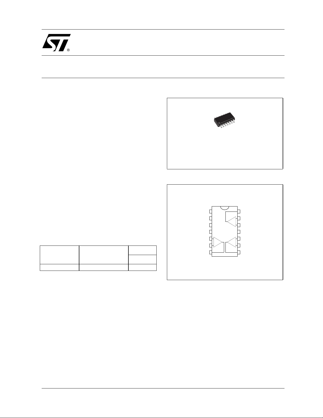
SO14
(Plastic Micropackage)
PIN CONNECTIONS (top view)
N.C.
N.C.
N.C.
V
CC
Non-inverting Input 1
Inverting Input 1
Output 1
1
2
3
+
4
5
+
-
6
7
14
13
-
+
12
11
10
+
9
8
Output 3
Inverting Input 3
Non-inverting Input 3
-
V
CC
Non-inverting Input 2
Inverting Input 2
Output 2
D = Small Outline Package (SO) - also available i n Tape & Reel (DT)
October 2000
1/8
Page 2

TSH93
SCHEMATIC DIAGRAM (1/3)
non inverting
input
V
CC
Internal
V
ref
+
output
inverting
input
C
c
-
V
CC
MAXIMUM RATINGS
Symbol Parameter Value Unit
V
T
T
Supply Voltage
CC
V
Differential Input Voltage
id
V
i Input Voltage
Operating Free-Air Temperature range -40 to +125 °C
oper
Storage Temperature Range -65 to +150 °C
stg
1)
2)
3)
1. All voltages values, except differential voltage are with respect to network ground terminal
2. Dif ferential voltages are the non-inver ting input ter minal with respect to the inv erting input terminal
3. The magnitude of input and out put voltages m ust never exc eed V
CC
+
+0.3V
14 V
±5 V
-0.3 to 12 V
OPERATING CONDITIONS
Symbol Parameter Value Unit
V
Supply Voltage 7 to 12 V
CC
V
Common Mode Input Voltage Range
ic
V
CC
-
+2 to V
CC
+
-1
V
2/8
Page 3

ELECTRICAL CHARACTERISTICS
+
V
= 5V, V
CC
Symbol Parameter Min. Typ. Max. Unit
V
io
I
io
I
ib
I
CC
CMR
SVR
Avd
V
OH
V
OL
I
o
GBP
f
T
SR
e
n
m
φ
V
O1/VO2
Gf
THD
G
∆
∆ϕ
-
= -5V, T
CC
Input Offset Voltage
T
. ≤ T
min
Input Offset Current
. ≤ T
T
min
Input Bias Current
T
. ≤ T
min
Supply Current (per amplifier, no load)
. ≤ T
T
min
Common-mode Rejection Ratio V
T
. ≤ T
min
Supply Voltage Rejection Ratio V
. ≤ T
T
min
Large Signal Voltage Gain R
. ≤ T
T
min
= 25°C (unless otherwise specified)
amb
≤ T
amb
max.
≤ T
amb
max.
.
≤ T
amb
max.
≤ T
amb
max.
= -3V to +4V, Vo = 0V
= 100
L
ic
CC
= ±5V to ±3V
Vo = ±2.5V
Ω,
amb
amb
amb
≤ T
≤ T
≤ T
max.
max
max.
80
70
60
50
57
54
4
6
12
5
515
20
4.5 6
8
100
75
70
High Level Output Voltage Vid = 1V
R
= 600
Ω
L
= 150
R
. ≤ T
T
min
amb
≤ T
max.
RL = 150Ω
Ω
L
2.5
2.4
3
3.5
3
Low Level Output Voltage Vid = 11V
= 600
R
R
T
. ≤ T
min
amb
≤ T
max.
RL = 150Ω
L
= 150
L
Ω
Ω
-3.5
-2.8
-3
-2.5
-2.4
Output Short Circuit Current Vid = ±1V
Source
Sink
. ≤ T
T
min
amb
≤ T
max.
Source
Sink
20
20
15
15
36
40 mA
Gain Bandwidth Product
= 100, RL = 600Ω, CL = 15pF, f = 7.5MHz
A
VCL
90 150
Transition Frequency 90 MHz
Slew Rate
= -2 to +2V, A
V
in
Equivalent Input Voltage Noise Rs = 50Ω, f = 1kHz
Phase Margin A
VM
= +1
= +1, RL = 600
VCL
CL = 15pF
Ω,
62 110
4.2 nV/√Hz
35 Degrees
Channel Seperation f = 1MHz to 10MHz 65 dB
Gain Flatness f = DC to 6MHz, A
Total Harmonic Distortion f = 1kHz, V
Differential Gain f = 3.58MHz, A
Differential Phase f = 3.58MHz, A
= 10dB
VCL
= ±2.5V, RL = 600
o
= +2, RL = 150
VCL
= +2, RL = 150
VCL
0.1 dB
Ω
Ω
Ω
0.01 %
0.03 %
0.07 Degree
TSH93
mV
A
µ
A
µ
mA
dB
dB
dB
V
V
MHz
V/µs
3/8
Page 4

TSH93
PRINTED CIRCUIT LAYOUT
As for any high frequency device, a few rules m ust be ob served when des igning th e PCB t o get the best
performances from this high speed op amp.
From the most to the least important points :
❑ Each power supply lead has to be bypassed to ground with a 10nF ceramic capa citor very close
to the device and a 10µF capacitor.
❑ T o provide low inductance and low resistance common return, use a ground plane or common point
return for power and signal.
❑ All leads must be wide and as short as possible especially for op amp inputs. This is in order to
decrease parasitic capacitance and inductance.
❑ Use small resistor values to decrease time constant with parasitic capacitance.
❑ Choose component sizes as small as possible (SMD).
On output, decrease capacitor load so as to avoid circuit stability being degraded whic h may caus e
oscillation. You can also add a serial resistor in order to minimise its influence.
INPUT OFFSET VOLTAGE DRIFT VERSUS
TEMPERATURE
LARGE SIGNAL FOLLOWER RESPONSE
STATIC OPEN LOOP VOLTAGE GAIN
SMALL SIGNAL FOLLOWER RESPO N SE
4/8
Page 5

TSH93
OPEN LOOP FREQUENCY RESPONSE AND
PHASE SHIFT
AUDIO BANDWIDTH FREQUENCY
RESPONSE AND PHASE SHIFT
(TSH93 vs Standard 15MHz Audio Op-Amp)
CLOSE LOOP FREQUENCY RESPONSE
GAIN FLATNESS AND PHASE SHIF T VERSUS
FREQUENCY
CROSS TALK ISOLATION VERSUS
FREQUENCY (SO14 PACKAGE)
CROSS TALK ISOLATION VERSUS
FREQUENCY (SO14 PACKAGE)
5/8
Page 6

TSH93
DIFFERENTIAL INPUT IMPEDANCE VERSUS
FREQUENCY
4.5
4.0
3.5
3.0
)
W
2.5
2.0
Zin-diff (k
1.5
1.0
0.5
1k 10k 100k 1M 10M 100M
Frequency (Hz)
COMMON INPUT IMPEDANCE VERSUS
FREQUENCY
120
100
80
)
W
60
Zin-com (M
40
20
1k 10k 100k 1M 10M 100M
Frequency (Hz)
6/8
Page 7

MACROMODEL
Applies to: TSH93I
TSH93
** Standard Linear Ics Macromodels, 1997.
** CONNECTIONS :
* 1 INVERTING INPUT
* 2 NON-INVERTING INPUT
* 3 OUTPUT
* 4 POSITIVEPOWER SUPPLY
* 5 NEGATIVE POWER SUPPLY
.SUBCKT TSH93 1 3 2 4 5(analog)
********************************************************
.MODEL MDTH D IS=1E-8 KF=1.809064E-15
CJO=10F
* INPUT ST AGE
CIP 2 5 1.000000E-12
CIN 1 5 1.000000E-12
EIP 10 5 2 5 1
EIN 16 5 1 5 1
RIP 10 11 2.600000E-01
RIN 15 16 2.600000E-01
RIS 11 15 3.645298E-01
DIP 11 12 MDTH 400E-12
DIN 15 14 MDTH 400E-12
VOFP 12 13 DC 0.000000E+00
VOFN 13 14 DC 0
IPOL 13 5 1.000000E-03
CPS 11 15 2.986990E-10
DINN 17 13 MDTH 400E-12
VIN 17 5 2.000000e+00
DINR 15 18 MDTH 400E-12
VIP 4 18 1.000000E+00
FCP 4 5 VOFP 3.500000E+0 0
FCN 5 4 VOFN 3.500000E+00
FIBP 2 5 VOFP 1.000000E-02
FIBN 5 1 VOFN 1.000000E-02
* AMPLIFYING STAG E
FIP 5 19 VOFP 2.530000E+02
FIN 5 19 VOFN 2.530000E+02
RG1 19 5 3.160721E+03
RG2 19 4 3.160721E+03
CC 19 5 2.00000E-09
DOPM 19 22 MDTH 400E-12
DONM 21 19 MDTH 400E-12
HOPM 22 28 VOUT 1.504000E+03
VIPM 28 4 5.000000E+01
HONM 21 27 VOUT 1.400000E+03
VINM 5 27 5.000000E+01
*********** ************
RZP1 5 80 1E+06
RZP2 4 80 1E+06
GZP 5 82 19 80 2.5E-05
RZP2H 83 4 10000
RZP1H 83 82 80000
RZP2B 84 5 10000
RZP1B 82 84 80000
LZPH 4 83 3.535e-02
LZPB 84 5 3.535e-02
EOUT 26 23 82 5 1
VOUT 23 5 0
ROUT 26 3 35
COUT 3 5 30.000000E-12
DOP 19 25 MDTH 400E-12
VOP 4 25 2.361965E+00
DON 24 19 MDTH 400E-12
VON 24 5 2.361965E+00
.ENDS
ELECTRICAL CHARACTERISTICS
= ±5V, T
V
CC
Symbol Conditions Value Unit
V
io
A
vd
I
CC
V
icm
V
OH
V
OL
I
sink
I
sourceVo
GBP
SR
m
φ
= 25°C (unless otherwise specificed)
amb
0mV
RL = 600
No load / Ampli 5.2 mA
RL = 600
RL = 600
Vo = 0V
R
R
R
Ω
Ω
Ω
= 0V
= 600Ω, CL = 15pF
L
= 600Ω, CL = 15pF
L
= 600Ω, CL = 15pF
L
3.2 V/mV
-3 to 4 V
+3.6 V
-3.6 V
40 mA
40 mA
147 MHz
110 V/µs
42 Degrees
7/8
Page 8

TSH93
PACKAGE MECHANICAL DATA
14 PINS - PLASTIC MICROPACKAGE (SO)
Dim.
Millimeters Inches
Min. Typ. Max. Min. Typ. Max.
A 1.75 0.069
a1 0.1 0.2 0.004 0.008
a2 1.6 0.063
b 0.35 0.46 0.014 0.018
b1 0.19 0.25 0.007 0.010
C 0.5 0.020
c1 45° (typ.)
D (1) 8.55 8.75 0.336 0.344
E 5.8 6.2 0.228 0.244
e 1.27 0.050
e3 7.62 0.300
F (1) 3.8 4.0 0.150 0.157
G 4.6 5.3 0.181 0.208
L 0.5 1.27 0.020 0.050
M 0.68 0.027
S 8° (max.)
Note : (1) D and F do not i nclude mold flash or protrusions - Mold flash or protrusions shall not exceed 0.15mm (.066 inc) ONLY FOR DATA B OOK.
Information furnished is bel ieved to be accurate and reliable. However, STMicroe lectronics assumes no responsibility for the
consequences of use of such information nor for any infringement of patents or other rights of third parties which may result from
its use. No li cense is granted by imp lica tion or otherwise under an y patent or patent rig hts of STMicroelectronics. Specific at ions
mentioned in this publication ar e subject to change without notice. This publication supersedes and replaces all information
previously supplied. S TMicroelectronics products are not authorized for use as critica l components in life suppo rt devices or
systems without express written approval of STMicroelectronics.
© The ST logo is a registered trademark of STMicroelectronics
8/8
© 2000 STM icroelectronics - Printed in Ital y - All Rights Reserved
STMicr o el ectronics G ROU P OF COMPANIE S
Australi a - Brazil - Chi na - Finland - F rance - Germany - Hong Kon g - I ndi a - Italy - Jap an - Malaysia - Malta - Morocco
Singapo re - Spain - Sweden - Switzerland - Un i ted Kingdom
© http://www.st.com
 Loading...