

Page 1
.
1.5V to 5VOPERATINGVOLTAGE
.
28dB GAIN @ 3V @ 450MHz
.
20dB GAIN @ 3V @ 900MHz
.
+13.5dBmOUTPUTPOWER(P1dB)
.
BIASPIN FOR CURRENT ADJUST&
AMPLIFIERDISABLE
.
ADJUSTABLEOUTPUTPOWER
.
50Ω INPUT/OUTPUTMATCHING
.
FULLYGUARANTEEDAT2.7V
DESCRIPTION
TSH690 is a wide band RF amplifier, consistedof
2 stages, designed in advanced bipolar process
featuring 28dB gain and +13.5dBm output power
at 450MHzunder 3V. The pin 8 allowsan external
bias current adjust to tune the output power and
also to set the amplifier in power-down mode. This
powerfulamplifierisdedicatedtoequipsecuredRF
data transmitters as antennadrivers in ISM band
(reliable RF meter-readingsystems, secured Remote Controls, Cordless Telephones,...)
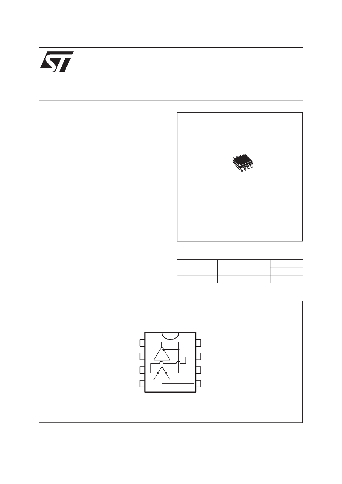
TSH690
40MHz to 1GHz AMPLIFIER
D
SO8
(Plastic Micropackage)
ORDER CODES
Part Number Temperature Range
o
TSH690ID -40, +85
C •
Package
D
PIN CONNECTIONS (top view)
RF out
September 1998
GND
GND
GND
1
2
3
4
8
7
6
5
Vbias
V
CC
GND
RF in
1/10
Page 2
TSH690
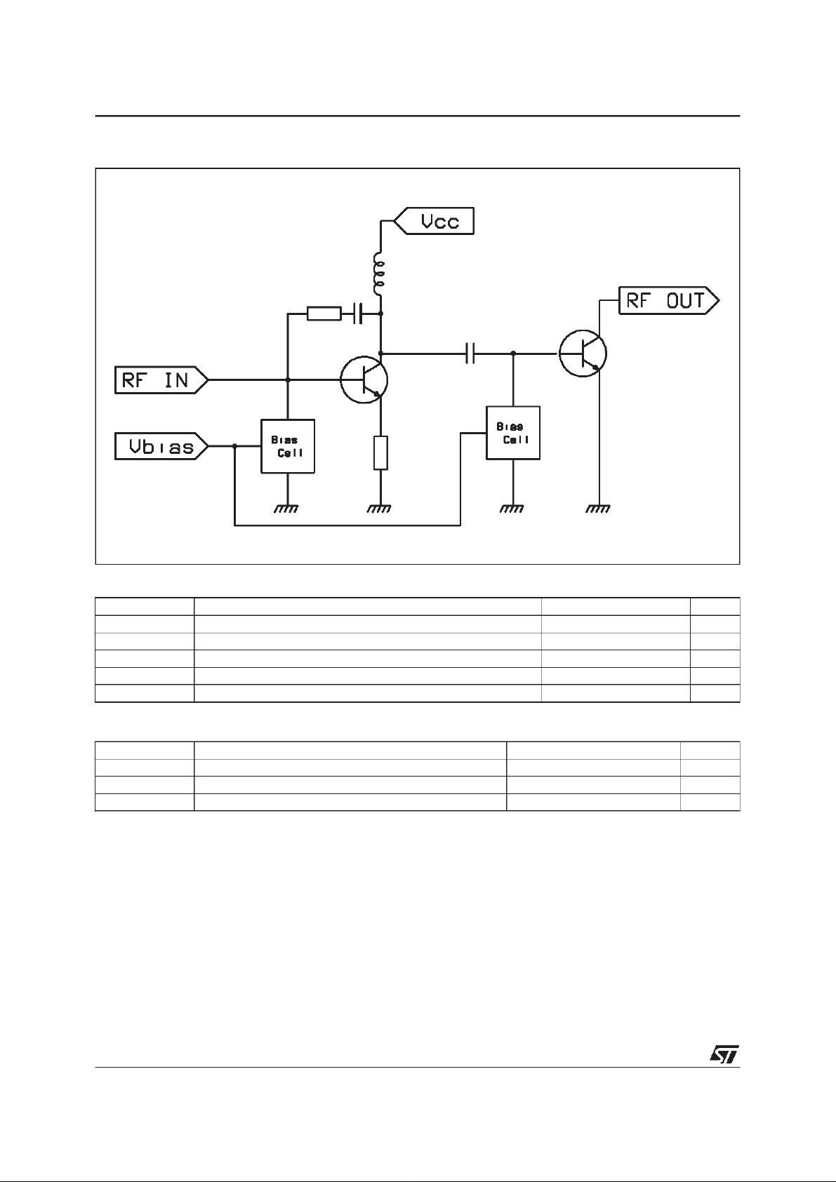
SCHEMATIC DIAGRAM
ABSOLUTE MAXIMUMRATINGS
Symbol Parameter Value Unit
V
CC1,VCC2,Vbias
RF in RF Input Power +10 dBm
RF out RF Output Power +21 dBm
T
oper
T
stg
Supply Voltages & Bias Voltage 5.5 V
Operating Free Air Temperature Range -40 to +85
Storage Temperature Range -65 to +150
OPERATINGCONDITIONS
Symbol Parameter Value Unit
V
CC1,VCC2
V
bias
RF
sr
Supply Voltages 1.5 to 5 V
Bias Voltage 0 to 6 V
RF SignalRange 40 to 1000 MHz
ESD SENSITIVEDEVICE
Handling Precautions Required
o
C
o
C
2/10
Page 3
ELECTRICAL CHARACTERISTICS
=25oC, VCC&V
T
amb
=+2.7V, ZL=50Ω
bias
TSH690
Parameter
SupplyCurrent 40 46 mA
S21 (V
S21 (Vin= -20dBm, f = 900MHz) 17 dB
Output Power 1dB Compression (f = 450MHz) 8 12 dBm
3rd Order Intercept Point (f = 430MHz) 16 22 dBm
S12 (Reverse Isolation @ f = 400MHz) -46 dB
S11 (Input Return Loss @f = 450MHz) -10 -15 dB
S11 (Input Return Loss @f = 900MHz) -10 dB
Noise Figure @ f = 450MHz 4.5 dB
Noise Figure @ f = 900MHz 5.4 dB
R
All parameters withmin. or max. figures are 100% tested.
= -20dBm, f = 450MHz) 20 23 30 dB
in
Junction Ambient ThermalResistance For SO8 Package 140 180
th(j-a)
Min. Typ. Max.
TSH690
o
SO8 PACKAGE THERMALRESISTIVITY
Tamb (°C)
150
135
120
105
90
75
60
45
30
DEVICE
OVERSTRESSED
RIGHT BEHAVIOUR
Rthmin
Rthmax
Unit
C/W
123456
DEFINITION
R
th(j-a)
(oC) Maximum Die JunctionTemperature
T
j
T
amb
P
(W) Maximum Dissipated Power
d
JunctionAmbient ThermalResistance
o
(~ 150
C)
(oC) Ambient Temperature
(P
= 0.75 VCC• ICC)
d
Vcc (V)
REMARKS
The rightbehaviour is obtained when the following equation is fulfilled.
T
j-Tamb=Pd•Rth(j-a)
3/10
Page 4

TSH690
TYPICALSCATTERINGPARAMETERS (Reference wavesplanes at package leads)
TEST CONDITIONS V
Freq S11 S21 S12 S22
MHz Mag Ang Mag Ang Mag Ang Mag Ang
40 0.642 -22.0 6.319 5.0 0.003 -126.5 0.715 -54.7
50 0.615 -25.7 6.406 7.1 0.008 170.7 0.631 -64.7
100 0.537 -41.3 7.643 7.7 0.002 70.1 0.369 -91.3
150 0.490 -55.6 9.353 3.1 0.004 -141.9 0.253 -100.9
200 0.464 -68.0 11.502 -5.7 0.007 -117.3 0.202 -100.9
250 0.428 -79.0 13.856 -18.0 0.003 162.3 0.203 -92.7
300 0.413 -92.1 16.229 -33.4 0.005 142.1 0.209 -87.6
350 0.373 -101.5 18.019 -51.2 0.008 101.4 0.263 -89.4
400 0.334 -106.7 19.110 -70.1 0.008 115.2 0.326 -99.7
450 0.312 -111.5 19.159 -90.3 0.008 169.9 0.382 -112.1
500 0.290 -112.5 18.154 -108.0 0.008 111.5 0.395 -122.9
550 0.302 -114.5 16.778 -124.8 0.010 92.1 0.425 -130.0
600 0.324 -118.2 15.075 -140.5 0.015 93.6 0.424 -139.6
650 0.335 -122.9 13.482 -153.6 0.011 109.6 0.427 -150.8
700 0.349 -129.6 11.992 -165.5 0.011 101.7 0.425 -159.0
750 0.368 -135.0 10.750 -177.2 0.019 82.4 0.414 -169.5
800 0.366 -142.1 9.453 173.4 0.011 79.5 0.413 -177.8
850 0.373 -147.9 8.598 165.0 0.015 60.2 0.432 176.2
900 0.374 -154.1 7.783 155.8 0.013 89.7 0.438 166.4
950 0.381 -159.0 7.117 146.7 0.017 111.3 0.447 160.8
1000 0.377 -165.8 6.500 138.9 0.013 82.2 0.462 155.1
CC1,VCC2,Vbias
= +2V,Pin = -40dBm,T
amb
=25oC
4/10
Page 5

TSH690
TEST CONDITIONS V
Freq S11 S21 S12 S22
MHz Mag Ang Mag Ang Mag Ang Mag Ang
40 0.616 -23.3 9.237 6.2 0.002 -135.8 0.733 -56.9
50 0.595 -27.0 9.402 7.9 0.005 -169.5 0.651 -67.7
100 0.513 -43.4 11.263 6.5 0.006 -153.8 0.381 -101.7
150 0.470 -57.7 13.566 0.9 0.006 94.5 0.227 -119.1
200 0.436 -71.1 16.434 -8.6 0.007 155.8 0.156 -117.5
250 0.402 -82.2 19.416 -21.3 0.007 154.1 0.134 -100.3
300 0.382 -95.0 22.265 -36.6 0.005 7.2 0.135 -75.7
350 0.343 -103.3 24.337 -53.7 0.008 40.6 0.193 -78.0
400 0.302 -109.7 25.564 -71.8 0.010 125.9 0.269 -86.1
450 0.279 -114.8 25.594 -91.2 0.008 167.1 0.316 -100.6
500 0.271 -114.0 24.292 -108.3 0.011 120.2 0.356 -111.0
550 0.280 -116.1 22.527 -124.7 0.013 101.0 0.396 -119.3
600 0.306 -119.8 20.511 -140.1 0.005 89.9 0.404 -131.3
650 0.315 -125.5 18.282 -153.2 0.006 107.2 0.400 -142.6
700 0.330 -131.1 16.311 -165.1 0.007 78.9 0.406 -151.6
750 0.333 -136.2 14.604 -177.1 0.012 84.5 0.398 -160.4
800 0.343 -142.5 12.860 173.6 0.017 76.0 0.399 -170.5
850 0.346 -148.0 11.668 165.1 0.014 90.8 0.411 -178.8
900 0.354 -155.1 10.579 156.0 0.018 75.6 0.413 170.9
950 0.347 -159.6 9.652 147.0 0.013 66.6 0.439 165.2
1000 0.355 -166.2 8.775 139.2 0.018 75.3 0.459 157.3
CC1,VCC2,Vbias
= +3V,Pin = -40dBm,T
amb
=25oC
TESTCONDITIONS V
Freq S11 S21 S12 S22
MHz Mag Ang Mag Ang Mag Ang Mag Ang
40 0.614 -23.1 11.023 6.9 0.002 107.6 0.726 -54.4
50 0.590 -27.4 11.248 7.9 0.003 -111.3 0.646 -65.1
100 0.508 -44.6 13.262 4.5 0.004 -47.0 0.366 -97.6
150 0.465 -59.9 15.736 -2.0 0.006 -62.5 0.206 -110.4
200 0.429 -72.0 18.727 -11.5 0.003 97.7 0.130 -104.3
250 0.396 -83.4 21.837 -24.2 0.002 -135.5 0.108 -78.6
300 0.371 -94.7 24.804 -39.3 0.009 154.7 0.136 -56.7
350 0.335 -103.8 26.854 -56.0 0.006 135.2 0.191 -64.3
400 0.295 -109.9 28.077 -73.6 0.003 139.7 0.262 -75.2
450 0.275 -114.8 28.113 -92.5 0.010 97.0 0.321 -85.8
500 0.265 -114.8 26.710 -109.4 0.007 111.8 0.335 -98.2
550 0.282 -117.0 24.831 -125.5 0.007 93.8 0.389 -108.5
600 0.296 -120.3 22.620 -140.8 0.007 110.0 0.393 -121.0
650 0.314 -124.7 20.235 -154.1 0.005 85.1 0.402 -131.7
700 0.321 -131.5 18.081 -166.2 0.010 93.2 0.388 -143.9
750 0.334 -135.8 16.178 -178.0 0.012 106.1 0.390 -153.8
800 0.339 -143.8 14.235 172.5 0.010 74.1 0.377 -162.4
850 0.348 -149.4 12.941 164.1 0.014 57.9 0.392 -170.4
900 0.340 -157.5 11.693 154.9 0.014 80.2 0.402 179.5
950 0.352 -161.0 10.670 145.7 0.006 87.4 0.409 171.4
1000 0.341 -166.8 9.683 137.6 0.016 50.0 0.433 163.3
CC1,VCC2,Vbias
= +4V, Pin= -40dBm, T
amb
=25oC
5/10
Page 6

TSH690
Figure1 : Typical 300MHz-1000MHzBiasingCircuit
APPLICATIONSINFORMATION
CIRCUIT DESCRIPTION
TheTSH690is50Ω input/outputinternallymatched
from 300MHz to 1000MHz.Due to its open-collector structure, the output RF port must be tied to
Vcc2. The pin 8 allows a bias currentadjust to set
the output power and the gain.The circuit is packagedinSO8forthermaldissipationconsiderations.
MATCHING
Withinthe300-1000MHzband, althoughthecircuit
ismatched,the outputreturn losscan be improved
by adding a serial inductor (L2) between the RF
output and V
(56nH @ 450MHz and 10nH @
CC2
900MHz).Below300MHz, usingthe S-parameters
matrix, specific input/output matching networks
can be calculated to maximize electrical performances.
DC BLOCKING
Because input/output are respectivelyinternal/external biased, DC blocks (C1, C2) are recommended on both RF ports to guarantee a DC
isolationfromthenextcells.Above500MHz,100pF
issuggested whereasbelow, 1nF is better and far
below(less than 100MHz),10nF is prefered.
BIASING
The amplifier can operate in the range of 1.5V to
5Vand offersa bias current adjust function
(Vbiaspin) whichenables the trimming of theRF
output power(AB class Amplifier) by tuning a seriesvariableresistor (Rbias).
WhenVbiasis wired to the Vcc rail, the current
consumptionis maximized getting the best linearity (A class Amplifier) whereasbiasingto
Ground,the IC is setin powerdownmode.
For highersupply voltage than 4V to reach high
output power, the serial resistor (R1) is strongly
recommendedto increasethe efficiency of the
amplifierand thereforereduce the thermaldissipationof the circuit.
DECOUPLING
As withany RFdevices, the supplyvoltagedecoupling must be done carefully using a 1nF bypass
capacitor (C3, C5) placed as close as possible to
the device pins and could be also improved by
adding a 150nH RF choke inductance (L1). Concerningthe Vbiaspin, a 10nFdecouplingcapacitor
(C4)is recommendedwhileplacingon boardis not
critical.Note thatSurfaceMounted Devices(SMD)
componentsare prefered for RF applicationsdue
to theright behaviourin highfrequencieswhile low
inductor values (few 10nH) can be printed on
board.
6/10
Page 7

TSH690
GAIN vs FREQUENCY(450MHz)
30
25
20
Gain(dB)
15
L2 =10nH(450MHz Operation)
Vcc=Vbias=3V
10
100 200 300 400 500 600 700 800 900 1000
Freq (MHz)
INPUT RETURN LOSS (450MHz)
0
-5
-40°C
+25°C
V
+85°C
GAIN vs FREQUENCY(900MHz)
30
25
20
Gain(dB)
15
L2 =10nH (900MHz Operation)
Vcc=Vbias=3V
10
100 200 300 400 500 600 700 800 900 1000
Freq(MHz)
INPUTRETURN LOSS (900MHz)
0
-5
-40°C
+25°C
V
+85°C
2V
3V
S11(dB)
-10
-15
-20
Vcc=Vbias @ Ta=+25°C
L2=56nH (450MHz operation)
-25
100 200 300 400 500 600 700 800 900 1000
Freq(MHz)
OUTPUT RETURN LOSS (450MHz)
0
-5
3V
-10
S22(dB)
-15
-20
-25
100 200 300 400 500 600 700 800 900 1000
2V
Vcc=Vbias @ Ta=+25°C
L2=56nH (450MHz operation)
Freq(MHz)
-10
S11 (dB)
-15
4V
-20
Vcc=Vbias @ Ta=+25°C
2V
3V
4V
L2 =10nH(900MHz operation)
-25
100 200 300 400 500 600 700 800 900 1000
Freq (MHz)
OUTPUT RETURN LOSS (900MHz)
0
-5
-10
4V
S22 (dB)
-15
-20
Vcc=Vbias @ Ta=+25°C
L2=10nH (900MHz operation)
-25
100 200 300 400 500 600 700 800 900 1000
Freq (MHz)
3V
2V
4V
7/10
Page 8

TSH690
REVERSE ISOLATIONvs FREQUENCY
0
-10
-20
-30
S12 (dB)
-40
-50
L2=10nH
L2=56nH
Vcc=Vbias=3V
Ta=+25°C
-60
100 200 300 400 500 600 700 800 900 1000
Freq(MHz)
ADMISSION(900MHz)
20
15
+85°C
10
Pout (dBm)
-40°C
5
0
-20 -15 -10 -5 0
+25°C
Vcc=Vbias=3V
L2 =10nH (900MHz operation)
Pin (dBm)
1dB COMPRESSIONvs BIAS VOLTAGE
20
15
Vcc = 3V
10
P1dB(dBm)
5
0
1,5 2 2,5 3 3,5 4
Vcc= 2V
L2=10nH (900MHz operation)
Vbias(V)
Ta=25°C
SUPPLYCURRENT vs BIASVOLTAGE
60
Icctotal
40
Icctotal (mA)
20
Vcc=3V,Ta=+25°C
Pin= -40dBm
0
0 0,5 1 1,5 2 2,5 3
Vbias(V)
I bias
Vcc = 4V
6
4
I bias(mA)
2
0
8/10
Page 9

DEMONSTRATION BOARD : Diagram for 300MHz - 1000MHz operation
DEMONSTRATION BOARD : Silk Screen
TSH690
DEMONSTRATION BOARD : Printed Circuit Board (available on request)
9/10
Page 10

TSH690
PACKAGEMECHANICALDATA
8 PINS- PLASTICMICROPACKAGE(SO)
Dim.
Min. Typ. Max. Min. Typ. Max.
Millimeters Inches
A 1.75 0.069
a1 0.1 0.25 0.004 0.010
a2 1.65 0.065
a3 0.65 0.85 0.026 0.033
b 0.35 0.48 0.014 0.019
b1 0.19 0.25 0.007 0.010
C 0.25 0.5 0.010 0.020
c1 45
o
(typ.)
D 4.8 5.0 0.189 0.197
E 5.8 6.2 0.228 0.244
e 1.27 0.050
e3 3.81 0.150
F 3.8 4.0 0.150 0.157
L 0.4 1.27 0.016 0.050
M 0.6 0.024
S8
Information furnished is believed to be accurate and reliable. However, STMicroelectronics assumes no responsibility for the
consequences of use of such information nor for any infringement of patents or other rights of third parties which may result from
its use. No license is granted by implication or otherwise under any patent or patent rights of STMicroelectronics. Specifications
mentioned in this publication are subject to change without notice. This publication supersedes and replaces all information
previously supplied. STMicroelectronicsproducts are not authorized for useascritical components inlife support devices orsystems
without express written approval of STMicroelectronics.
The ST logo is a trademark of STMicroelectronics
1998 STMicroelectronics – Printed in Italy – All Rights Reserved
STMicroelectronics GROUP OF COMPANIES
Australia - Brazil - Canada - China - France - Germany - Italy - Japan - Korea - Malaysia - Malta - Mexico - Morocco
The Netherlands - Singapore - Spain - Sweden - Switzerland - Taiwan - Thailand - United Kingdom - U.S.A.
http://www.st.com
o
(max.)
10/10
PM-SO16.EPS
SO16.TBL
ORDERCODE :
 Loading...