

Page 1
TSH60,61,62,63,64
Wide-Band, Low-Power Operational Amplifiers
with Standby
■ 5V, ±5V specifications
■ Gain-bandwidth product: 60MHz
■ Slew-rate: 80V/µs
■ Output current: up to 45mA
■ Input/output rail-to-rail
■ Specified for 150Ω load
■ Low distortion, THD: 0.1%
■ SO packages
Description
The TSH6x series offers single, dual, triple and
quad operational amplifiers featuring high video
performances.
The TSH6x op-amps can be used in consumer
video applications, such as set-top boxes, DVD
players and recorders, or TVs, as either video
buffers or video line drivers. Their performances
guarantee excellent video quality, enhancing the
performance of your video solution.
Running at single supply voltage from 5V to 12V,
amplifiers feature large output voltage swing and
high output current capability to drive standard
150Ω loads.
The TSH61 and TSH63 also feature standby
inputs, allowing the op amps to be put into a
standby mode with low power consumption and
high output impedance.
For easy integration into video applications, the
TSH6x series is proposed in standard SO8 and
SO14 packages.
Applications
■ Standard definition video buffers
■ Set-top boxes
■ DVD players and recorders
■ Analog and digital TVs
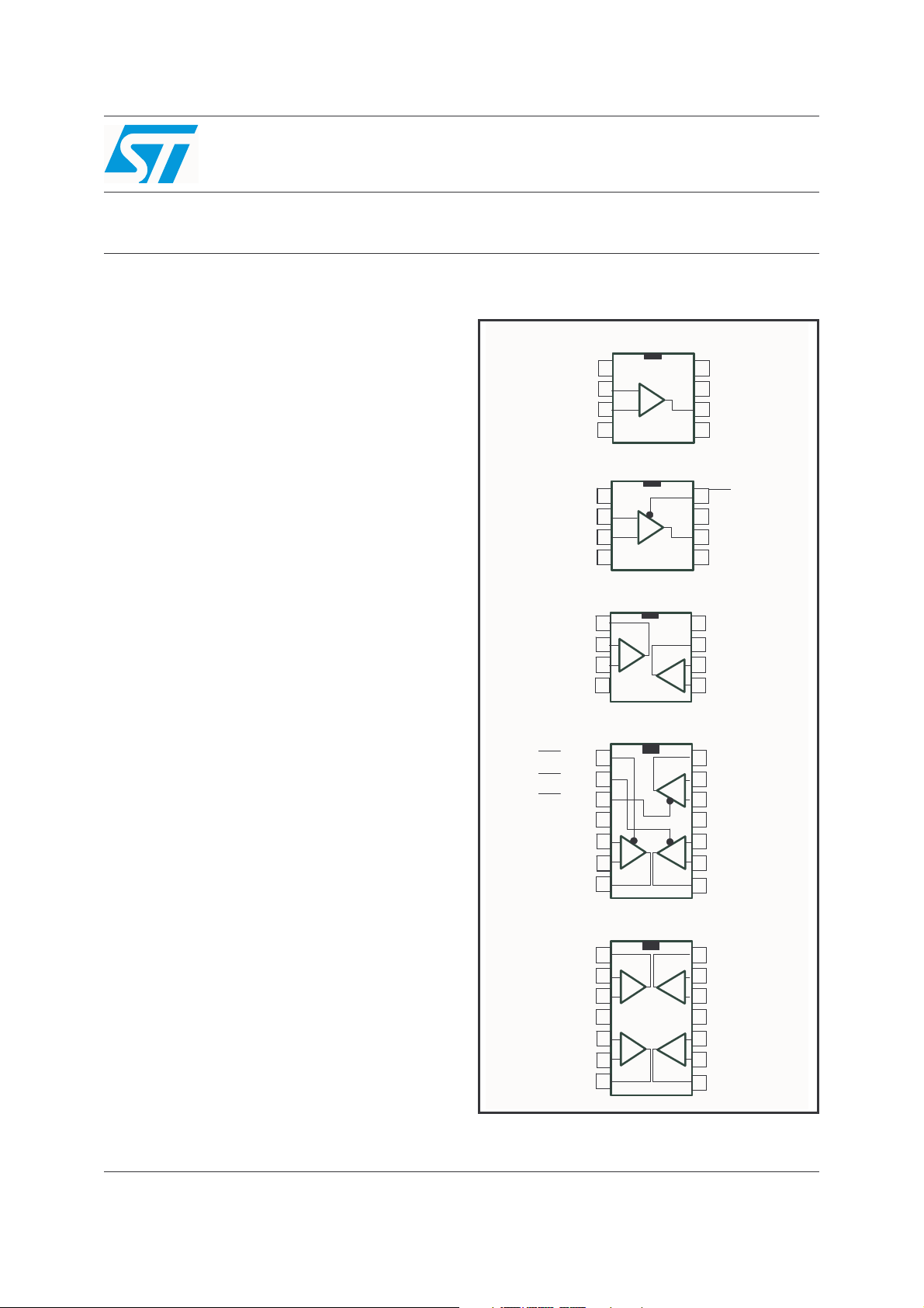
Pin connections (top view)
TSH60 : SO8
TSH60 : SO8
NC
NC
NC
NC
NC
1
1
1
_
_
_
2
2
Inverting Input
Inverting Input
Inverting Input
Non Inverting Input
Non Inverting Input
Non Inverting Input
Inverting Input
Inverting Input
Inverting Input
Non Inverting Input
Non Inverting Input
Non Inverting Input
Inverting Inpu t1 Outpu t2
Inverting Inpu t1 Outpu t2
Inverting Inpu t1 Outpu t2
Non Inverting Input1
Non Inverting Input1
Non Inverting Input1
STANDBY1
STANDBY1
STANDBY1
STANDBY2
STANDBY2
STANDBY2
STANDBY3
STANDBY3
STANDBY3
Non Inverting Input1
Non Inverting Input1
Non Inverting Input1
Inverting Input1
Inverting Input1
Inverting Input1
Inverting Input1
Inverting Input1
Inverting Input1
Non Inverting Input1
Non Inverting Input1
Non Inverting Input1
Non Inverting Input2
Non Inverting Input2
Non Inverting Input2
Inverting Input2
Inverting Input2
Inverting Input2
2
3
3
3
VCC -
VCC -
VCC -
4
4
4
TSH61 : SO8
TSH61 : SO8
NC
NC
NC
1
1
1
2
2
2
3
3
3
VCC -
VCC -
VCC -
4
4
4
TSH62 : SO8
TSH62 : SO8
Output1
Output1
Output1
1
1
1
2
2
2
3
3
3
VCC -
VCC -
VCC -
4
4
4
TSH63 : SO14
TSH63 : SO14
1
1
1
2
2
2
3
3
3
VCC +
VCC +
VCC +
5
5
5
6
6
6
7
7
7
Output1
Output1
Output1
TSH64 : SO14
TSH64 : SO14
1
1
1
Output1
Output1
Output1
2
2
2
3
3
3
VCC +
VCC +
VCC +
5
5
5
6
6
6
Output2
7
Output2
7
Output2
7
+
+
+
_
_
_
+
+
+
_
_
_
+
+
+
+
+
+
_
_
_
_
_
_
+
+
+
+
+
+
_
_
_
NC
8
8
8
7
7
7
VCC +
VCC +
VCC +
6
Output
6
Output
6
Output
NC
NC
NC
5
5
5
8
8
8
STANDB Y
STANDB Y
STANDB Y
7
7
7
VCC +
VCC +
VCC +
6
Output
6
Output
6
Output
NC
NC
NC
5
5
5
VCC +
VCC +
VCC +
8
8
8
7
7
7
Inverting Input2
Inverting Input2
Inverting Input2
_
_
_
6
6
6
+
+
+
Non Inverting Input2
Non Inverting Input2
Non Inverting Input2
5
5
5
14
14
14
Output3
Output3
Output3
13
13
13
Inverting Input3
Inverting Input3
Inverting Input3
_
_
_
+
+
+
Non Inverting Input3
Non Inverting Input3
Non Inverting Input3
12
12
12
VCC -
VCC -
VCC -
114
114
114
10
10
10
Non Inverting Input2
Non Inverting Input2
Non Inverting Input2
+
+
+
_
_
_
Inverting Input2
Inverting Input2
Inverting Input2
9
9
9
Output2
Output2
Output2
8
8
8
14
14
14
Output4
Output4
Output4
13
13
13
Inverting Input4
Inverting Input4
Inverting Input4
_
_
_
+
+
+
Non Inverting Input4
Non Inverting Input4
Non Inverting Input4
12
12
12
114
114
114
VCC -
VCC -
VCC -
10
10
10
Non Inverting Input3
Non Inverting Input3
Non Inverting Input3
+
+
+
_
_
_
Inverting Input3
Inverting Input3
Inverting Input3
9
9
9
Output3
Output3
Output3
8
8
8
March 2006 Rev. 1 1/13
www.st.com
13
Page 2

Order Codes TSH60,61,62,63,64
1 Order Codes
Type Temperature Range Packages Packing Marking
TSH60CD/CDT
TSH61CD/CDT TSH61C
TSH62CD/CDT TSH62C
TSH63CD/CDT
TSH64CD/CDT TSH64C
0°C to 70°C
SO8
Tube or Tape & Reel
SO14
TSH60C
TSH63C
2/13
Page 3
TSH60,61,62,63,64 Absolute Maximum Ratings and Operating Conditions
2 Absolute Maximum Ratings and Operating
Conditions
Table 1. Absolute maximum ratings
Symbol Parameter Value Unit
(3)
(1)
(2)
(4)
14 V
±2V
±6V
28
°C/W
22
157
°C/W
125
T
V
T
R
R
CC
V
V
oper
stg
T
thjc
thja
Supply Voltage
id
i
Differential Input Voltage
Input Voltage
Operating Free Air Temperature Range 0 to +70 °C
Storage Temperature -65 to +150 °C
j
Maximum Junction Temperature 150 °C
Thermal Resistance Junction to Case
SO8
SO14
Thermal Resistance Junction to Ambiant Area
SO8
SO14
ESD HumanBodyModel 2 kV
1. All voltages values, except differential voltage are with respect to network ground terminal
2. Differential voltages are non-inverting input terminal with respect to the inverting terminal
3. The magnitude of input and output must never exceed VCC +0.3V
4. Short-circuits can cause excessive heating
Table 2. Operating conditions
Symbol Parameter Value Unit
V
CC
V
IC
Supply Voltage 4.5 to 12 V
Common Mode Input Voltage Range V
CC
-
to (V
+
-1.1) V
CC
3/13
Page 4
Standby Mode TSH60,61,62,63,64
3 Standby Mode
Table 3. V
+
(positive supply voltage), V
CC
-
(negative supply voltage, or ground), T
CC
amb
= 25°C
(unless otherwise specified)
Symbol Parameter Test Conditions Min. Typ. Max. Unit
Vl
ow
V
high
I
CC STBY
Z
out
T
on
T
off
Standby Low Level V
Standby High Level (V
Current Consumption per
Operator when STANDBY is
Active
Output Impedance (Rout//Cout)
pin 8 (TSH61) to V
pin 1,2 or 3 (TSH63) to V
R
out
C
out
CC
-
CC
CC
-
Time from Standby Mode to
Active Mode
Time from Active Mode to
Standby Mode
TSH61 Standby Control pin 8 (STBY
V
low
V
high
Down to I
CC STBY
= 10µA10 µs
) Operator Status
TSH63 Standby Control Operator Status
-
CC
-
+2) (V
20 55 µA
10
17
2 µs
Standby
Active
(V
CC
-
+0.8) V
+
)V
CC
MΩ
pF
pin 1
(STBY
OP1)
V
low
V
high
xV
xV
xxV
xxV
pin 2
(STBY OP2)
pin 3
(STBY OP3)
x x Standby x x
xxActivexx
low
high
x x Standby x
low
high
OP1 OP1 OP3
xActivex
x x Standby
xxActive
4/13
Page 5

TSH60,61,62,63,64 Electrical Characteristics
4 Electrical Characteristics
Table 4. V
CC
+
= 5V, V
-
= GND, Vic = 2.5V, T
CC
= 25°C (unless otherwise specified)
amb
Symbol Parameter Test Conditions Min. Typ. Max. Unit
= 25°C
T
| Input Offset Voltage
|V
io
I
Input Bias Current 6 µA
ib
Input Capacitance 0.3 pF
C
in
I
Supply Current per Operator
CC
CMRR
PSRR
Common Mode Rejection Ratio
(δVic/δVio)
Power Supply Rejection Ratio
(δVCC/δVout)
A
Large Signal Voltage Gain
vd
Output Short Circuit Current Source
I
o
amb
T
< T
min.
amb
+0.1 < Vic < 3.9V & Vout = 2.5V 85 dB
Positive & Negative Rail 70 dB
=150Ω to 1.5V
R
L
V
=1V to 4V 78
out
= +1, V
V
id
V
id
= -1, V
out
out
|Source|
Sink
= 150Ω to GND
R
V
High Level Output Voltage
oh
Low Level Output Voltage
V
ol
Bw Bandwidth @-3dB
SR Slew Rate
φm Phase Margin R
THD Total Harmonic Distortion
∆G Differential gain
Df Differential phase
L
R
= 150Ω to 2.5V
L
= 150Ω to GND
R
L
R
= 150Ω to 2.5V
L
= +1
A
VCL
R
=150Ω to 2.5V
L
= +2
A
VCL
R
=150Ω to 2.5V 86
L
=150Ω to 2.5V 40 °
L
= +2, F = 4MHz
A
VCL
R
=150Ω to 2.5V
L
V
= 1Vpp
out
V
= 2Vpp
out
A
= +2, RL = 150Ω to 2.5V
VCL
F = 4.5MHz, V
A
= +2, RL=150Ω to 2.5V
VCL
F = 4.5MHz, V
Gf Gain Flatness F= DC to 6MHz, A
< T
max.
to 1.5V
to 1.5V
out
out
= 2Vpp
= 2Vpp
= +2 0.2 dB
VCL
1.5 10
12
8.2
45
45
4.36
4.66
48
100
220
400
60 MHz
V/µs
-57
-51
0.5 %
0.5 °
mV
mA
mA
mV
Vo1/Vo2 Channel Separation F=1MHz to 10MHz 65 dB
dB
V
dB
5/13
Page 6

Electrical Characteristics TSH60,61,62,63,64
Table 5. V
CC
+
= 5V, V
-
= -5V, Vic = GND, T
CC
= 25°C (unless otherwise specified)
amb
Symbol Parameter Test Condition Min. Typ. Max. Unit
| Input Offset Voltage
|V
io
I
ib
C
in
I
CC
CMRR
PSRR
A
vd
I
o
Input Bias Current 6 µA
Input Capacitance 0.7 pF
Supply Current per Operator 9.8 mA
Common Mode Rejection Ratio
(δVic/δVio)
Power Supply Rejection Ratio
(δVCC/δVou t)
Large Signal Voltage Gain
Output Short Circuit Current Source
T
min.
< T
amb
< T
-4.9 <Vic < 3.9V & Vout = GND 94 dB
Positive & Negative Rail 70 dB
=150Ω to GND
R
L
V
=- 4 to +4 80
out
V
= +1, V
id
V
id
=- 1, V
out
out
|Source|
Sink
V
High Level Output Voltage RL = 150Ω to GND 4.36 V
oh
V
Low Level Output Voltage RL = 150Ω to GND -4.63 -4.4 mV
ol
= +1
A
Bw Bandwidth @-3dB
SR Slew Rate
φmPhase Margin R
THD Total Harmonic Distortion
∆G Differential gain
Df Differential phase
VCL
R
= 150Ω to GND
L
= +2
A
VCL
R
=150Ω to GND 98
L
= 150Ω to GND 40 °
L
= +2, F = 4MHz
A
VCL
R
=150Ω to GND
L
V
= 1Vpp
out
V
= 2Vpp
out
A
= +2, RL = 150Ω to GND
VCL
F = 4.5MHz, V
= +2, RL=150Ω to GND
A
VCL
F = 4.5MHz, V
Gf Gain Flatness F = DC to 6MHz, A
max.
to 1.5V
to 1.5V
= 2Vpp
out
= 2Vpp
out
1.2 10
12
45
45
74 MHz
-57
-51
0.5 %
0.5 °
= +2 0.2 dB
VCL
mV
mA
V/µs
Vo1/Vo2 Channel Separation F = 1MHz to 10MHz 65 dB
dB
dB
6/13
Page 7

TSH60,61,62,63,64 Electrical Characteristics
Figure 1. Closed loop gain and phase vs.
frequency (Gain = +2, V
R
=150Ω, T
10
5
0
-5
Gain (dB)
-10
-15
1E+4 1E+5 1E+6 1E+7 1E+8 1E+9
L
Frequency (Hz)
amb
Gain
Phase
= 25°C)
= ±2.5V,
CC
200
100
0
Phase (°)
-100
-200
Figure 3. Large signal measurement - positive
slew rate (Gain = 2, V
R
= 150Ω//5.6pF, Vin = 1Vpk)
L
3
2
= ±2.5V,
CC
Figure 2. Standby mode - Ton, Toff
= ±2.5V, open loop)
(V
CC
3
2
1
0
-1
Vin, Vout (V)
-2
-3
0 2E-6 4E-6 6E-6 8E-6 1E-5
Ton Toff
Vout
Standby
Vin
Time (s)
Figure 4. Large signal measurement -
negative slew rate (Gain = 2,
VCC= ±2.5V, RL = 150Ω//5.6pF,
Vin = 1Vpk)
3
2
1
0
Vout (V)
-1
-2
-3
0 1020304050607080
Time (ns)
Figure 5. Small signal measurement - rise
time (Gain = 2, V
Z
= 150Ω, Vin = 25mVpk)
L
Vin
0 102030405060
Tim e (ns)
Vin, Vout (V)
0.06
0.04
0.02
0
-0.02
-0.04
-0.06
Vout
= ±2.5V,
CC
1
0
Vout (V)
-1
-2
-3
0 10203040506070
Time (ns)
Figure 6. Small signal measurement - fall time
(Gain = 2, V
= ±2.5V, ZL = 150Ω,
CC
Vin = 25mVpk)
0.06
0.04
0.02
0
Vin Vout (V)
-0.02
-0.04
-0.06
0 102030405060
Vin
Vout
Time (ns)
7/13
Page 8

Electrical Characteristics TSH60,61,62,63,64
Figure 7. Equivalent noise voltage
(Gain = 100, V
30
+
25
20
Hz)
√
15
en (nV/
10
5
0.1 1 10 100 1000
_
10k
100
Frequency (kHz)
= ±2.5V, no load)
CC
Figure 8. Maximum output swing
(Gain = 11, VCC= ±2.5V, RL = 150Ω)
3
2
1
0
Vin, Vout (V)
-1
-2
-3
0.0E+0 5.0E-2 1.0E-1 1.5E-1 2.0E-1
Vout
Vin
Time (ms)
8/13
Page 9

TSH60,61,62,63,64 Video Applications
5 Video Applications
TSH6x operational amplifiers can be used to buffer standard definition video signals on
75-ohm video lines. An example of a video channel is shown below. A typical third-order
filter and its response are also shown.
Figure 9. Implementation of a video driver on a video DAC output
Video
DAC
1Vpp
Video
Signal
Reconstruction
LPF
1Kohm
Filter
1.05V
50mV
time
+5V
+
TSH6x
_
1Kohm
Volt
Video
Signal
2.1V
time
100mV
75Ω
2Vpp
Volt
75Ω Cable
Video
Signal
1.05V
50mV
75Ω
time
1Vpp
Figure 10. Third order low-pass filter and its response (for standard definition video)
5pF
5pF
Vin Vout
Vin Vout
6.8uH
6.8uH
33pF
33pF
33pF
33pF
9/13
Page 10

Package Mechanical Data TSH60,61,62,63,64
6 Package Mechanical Data
In order to meet environmental requirements, ST offers these devices in ECOPACK®
packages. These packages have a Lead-free second level interconnect. The category of
second level interconnect is marked on the package and on the inner box label, in
compliance with JEDEC Standard JESD97. The maximum ratings related to soldering
conditions are also marked on the inner box label. ECOPACK is an ST trademark.
ECOPACK specifications are available at: www.st.com.
6.1 SO-8 package
SO-8 MECHANICAL DATA
DIM.
A 1.35 1.75 0.053 0. 069
A1 0.10 0.25 0.04 0. 010
A2 1.10 1.65 0.043 0.065
B 0.33 0.51 0.013 0. 020
C 0.19 0.25 0.007 0.010
D 4.80 5.00 0.189 0.197
E 3.80 4.00 0.150 0. 157
e 1.27 0.050
H 5.80 6.20 0.228 0.244
h 0.25 0.50 0.010 0.020
L 0.40 1.27 0.016 0.050
k ˚ (max.)
ddd 0.1 0.04
MIN. TYP MAX. MIN. TYP. MAX.
mm. inch
8
10/13
0016023/C
Page 11

TSH60,61,62,63,64 Package Mechanical Data
6.2 SO-14 package
SO-14 MECHANICAL DATA
DIM.
A 1.75 0.068
a1 0.1 0.2 0.003 0.007
a2 1.65 0.064
b 0.35 0.46 0.013 0.018
b1 0.19 0.25 0.007 0.010
C 0.5 0.019
c1 45˚ (typ.)
D 8.55 8.75 0.336 0.344
E 5.8 6.2 0.228 0.244
e 1.27 0.050
e3 7.62 0.300
F 3.8 4.0 0.149 0.157
G 4.6 5.3 0.181 0.208
L 0.5 1.27 0.019 0.050
M 0.68 0.026
S˚ (max.)
MIN. TYP MAX. MIN. TYP. MAX.
mm. inch
8
PO13G
11/13
Page 12

Revision History TSH60,61,62,63,64
7 Revision History
Table 6. Document revision history
Date Revision Changes
March 2006 1 First Release.
12/13
Page 13

TSH60,61,62,63,64 Revision History
y
y
Please Read Carefully:
Informatio n in this document is provided solely in connection with ST products. STMicroelectronics NV and its subsidiaries (“ST”) reserve the
right to make changes, corrections, modifications or improvements, to this document, and the products and services described herein at an
time, without notice.
All ST products are sold pursuant to ST’s terms and conditions of sale.
Purchasers are solely responsible for the choice, selection and use of the ST products and services described herein, and ST assumes no
liability whatsoever relating to the choice, selection or use of the ST products and services described herein.
No license, express or implied, by estoppel or otherwise, to any intellectual property rights is granted under this document. If any part of this
document refers to any third party products or services it shall not be deemed a license grant by ST for the use of such third party products
or services, or any intellectual property contained therein or considered as a warranty covering the use in any manner whatsoever of such
third party products or services or any intellectual property contained therein.
UNLESS OTHERWISE SET FORTH IN ST’S TERMS AND CONDITIONS OF SALE ST DISCLAIMS ANY EXPRESS OR IMPLIED
WARRANTY WITH RESPECT TO THE USE AND/OR SALE OF ST PRODUCTS INCLUDING WITHOUT LIMITATION IMPLIED
WARRANTIES OF MERCHANTABILITY, FITNESS FOR A PARTICULAR PURPOSE (AND THEIR EQUIVALENTS UNDER THE LAWS
OF ANY JURISDICTION), OR INFRINGEMENT OF ANY PATENT, COPYRIGHT OR OTHER INTELLECTUAL PROPERTY RIGHT.
UNLESS EXPRESSLY APPROVED IN WRITING BY AN AUTHORIZE REPRESENTATIVE OF ST, ST PRODUCTS ARE NOT DESIGNED,
AUTHORIZED OR WARRANTED FOR USE IN MILITARY, AIR CRAFT, SPACE, LIFE SAVING, OR LIFE SUSTAINING APPLICATIONS,
NOR IN PRODUCTS OR SYSTEMS, WHERE FAILURE OR MALFUNCTION MAY RESULT IN PERSONAL INJURY, DEATH, OR
SEVERE PROPERTY OR ENVIRONMENTAL DAMAGE.
Resale of ST products with provisions different from the statements and/or technical features set forth in this document shall immediately void
any warranty granted by ST for the ST product or service described herein and shall not create or extend in any manner whatsoever, an
liability of ST.
ST and the ST logo are trademarks or registered trademarks of ST in various countries.
Information in this document supersedes and replaces all information previously supplied.
The ST logo is a registered trademark of STMicroelectronics. All other names are the property of their respective owners.
© 2006 STMicroelectronics - All rights reserved
STMicroelectronics group of companies
Australia - Belgium - Brazil - Canada - China - Czech Republic - Finland - France - Germany - Hong Kong - India - Israel - Italy - Japan -
Malaysia - Malta - Morocco - Singapore - Spain - Sweden - Switzerland - United Kingdom - United States of America
www.st.com
13/13
 Loading...