

Page 1
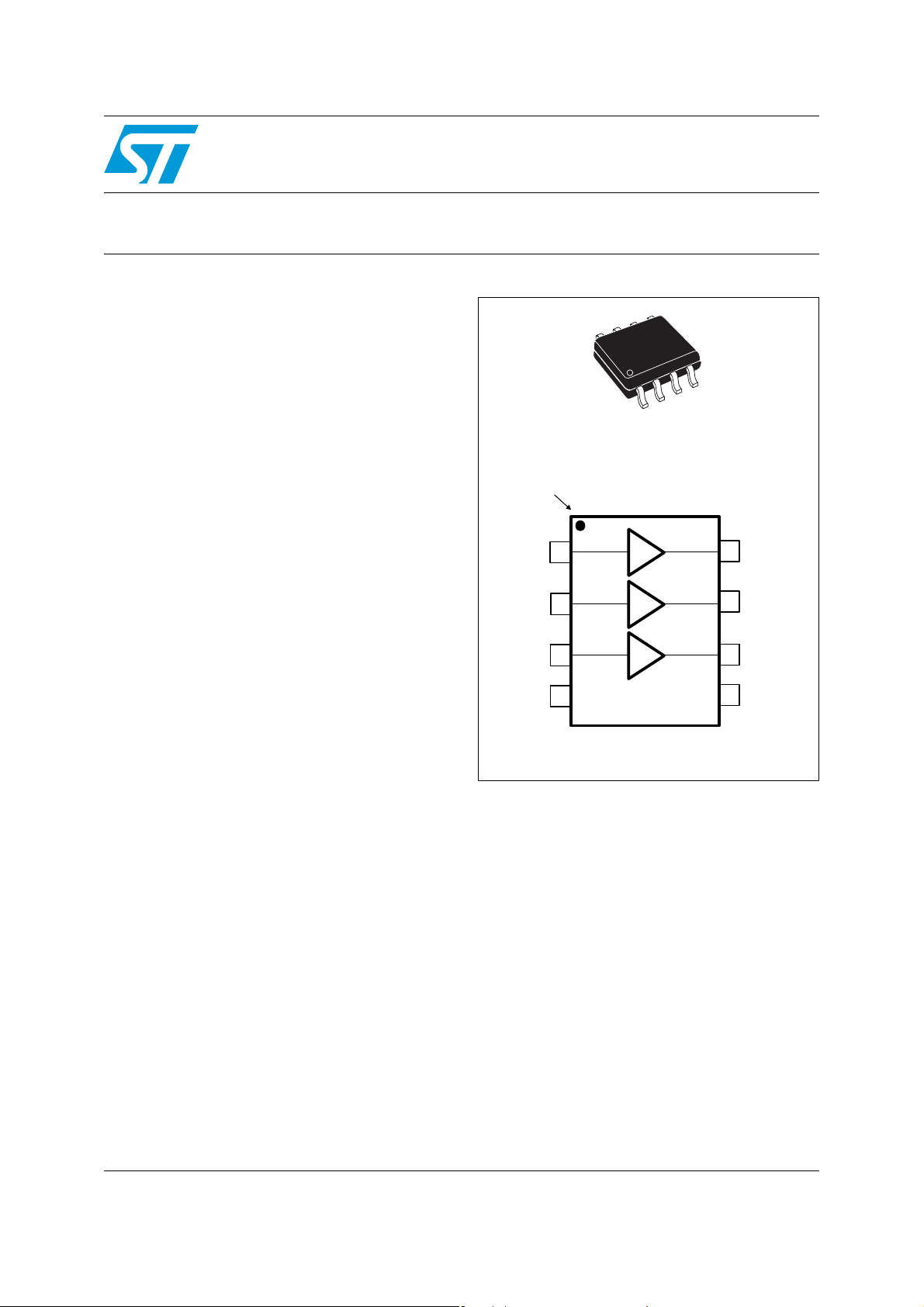
340MHz single-supply triple video buffer
Features
■ Bandwidth: 340MHz
■ 5V single-supply operation
■ Low output rail guaranteed at 60mV max
■ Internal gain of 6dB for a matching between 3
channels
■ Very low harmonic distortion
■ Slew rate: 740V/ms
■ Specified for 150Ω and 100Ω loads
■ Tested on 5V power supply
■ Min. and max. data tested during production
Pin connections (top view)
Pin1 identification
1
IN1
Top View
6dB
TSH344
8
OUT1
Applications
■ High-end video systems
■ High definition TV (HDTV)
■ Broadcast and graphic video
■ Multimedia products
Description
The TSH344 is a triple single-supply video buffer
featuring an internal gain of 6dB and a large
bandwidth of 340MHz.
The main advantage of this buffer is its very low
output rail very close to GND when supplied in
single supply 0/5V. This output rail is guaranteed
by test at 60mV from GND on 150Ω.
datasheet gives technical information on using
the TSH344 as an RGB driver for video DAC
output on a video line. See the TSH343 datasheet
for Y-Pb-Pr signals.
The TSH344 is available in the compact SO8
plastic package for optimum space-saving.
This
IN2
IN3
+Vcc
7
6
5
OUT2
OUT3
GND
2
3
4
6dB
6dB
SO8
March 2007 Rev 4 1/17
www.st.com
17
Page 2

Contents TSH344
Contents
1 Absolute maximum ratings and operating conditions . . . . . . . . . . . . . 3
2 Electrical characteristics . . . . . . . . . . . . . . . . . . . . . . . . . . . . . . . . . . . . . 4
3 Application information . . . . . . . . . . . . . . . . . . . . . . . . . . . . . . . . . . . . . 10
3.1 Using the TSH344 to drive R-G-B video components . . . . . . . . . . . . . . . 10
3.2 Power supply considerations . . . . . . . . . . . . . . . . . . . . . . . . . . . . . . . . . . 12
3.3 Delay between channels . . . . . . . . . . . . . . . . . . . . . . . . . . . . . . . . . . . . . 13
4 Package information . . . . . . . . . . . . . . . . . . . . . . . . . . . . . . . . . . . . . . . . 14
5 Ordering information . . . . . . . . . . . . . . . . . . . . . . . . . . . . . . . . . . . . . . . 16
6 Revision history . . . . . . . . . . . . . . . . . . . . . . . . . . . . . . . . . . . . . . . . . . . 16
2/17
Page 3
TSH344 Absolute maximum ratings and operating conditions
1 Absolute maximum ratings and operating conditions
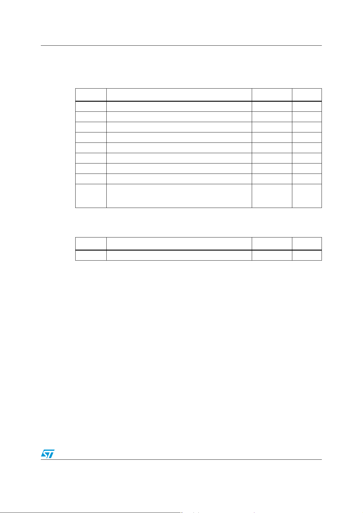
Table 1. Absolute maximum ratings (AMR)
Symbol Parameter Value Unit
V
T
T
R
R
P
CC
V
oper
stg
T
thjc
thja
max
Supply voltage
Input voltage range
in
Operating free air temperature range -40 to +85 °C
Storage temperature -65 to +150 °C
Maximum junction temperature 150 °C
j
SO8 thermal resistance junction to case 28 °C/W
SO8 thermal resistance junction to ambient area 157 °C/W
Maximum power dissipation (@T
CDM: charged device model
ESD
HBM: human body model
MM: machine model
1. All voltage values, except differential voltage, are with respect to network terminal.
2. The magnitude of input and output voltage must never exceed VCC +0.3V.
Table 2. Operating conditions
(1)
(2)
6V
0 to +2 V
=25°C) for Tj=150°C 800 mW
amb
2
1.5
200
kV
kV
V
Symbol Parameter Value Unit
V
CC
1. Tested in full production at 0V/5V single power supply.
Power supply voltage
(1)
3 to 5.5 V
3/17
Page 4
Electrical characteristics TSH344
2 Electrical characteristics
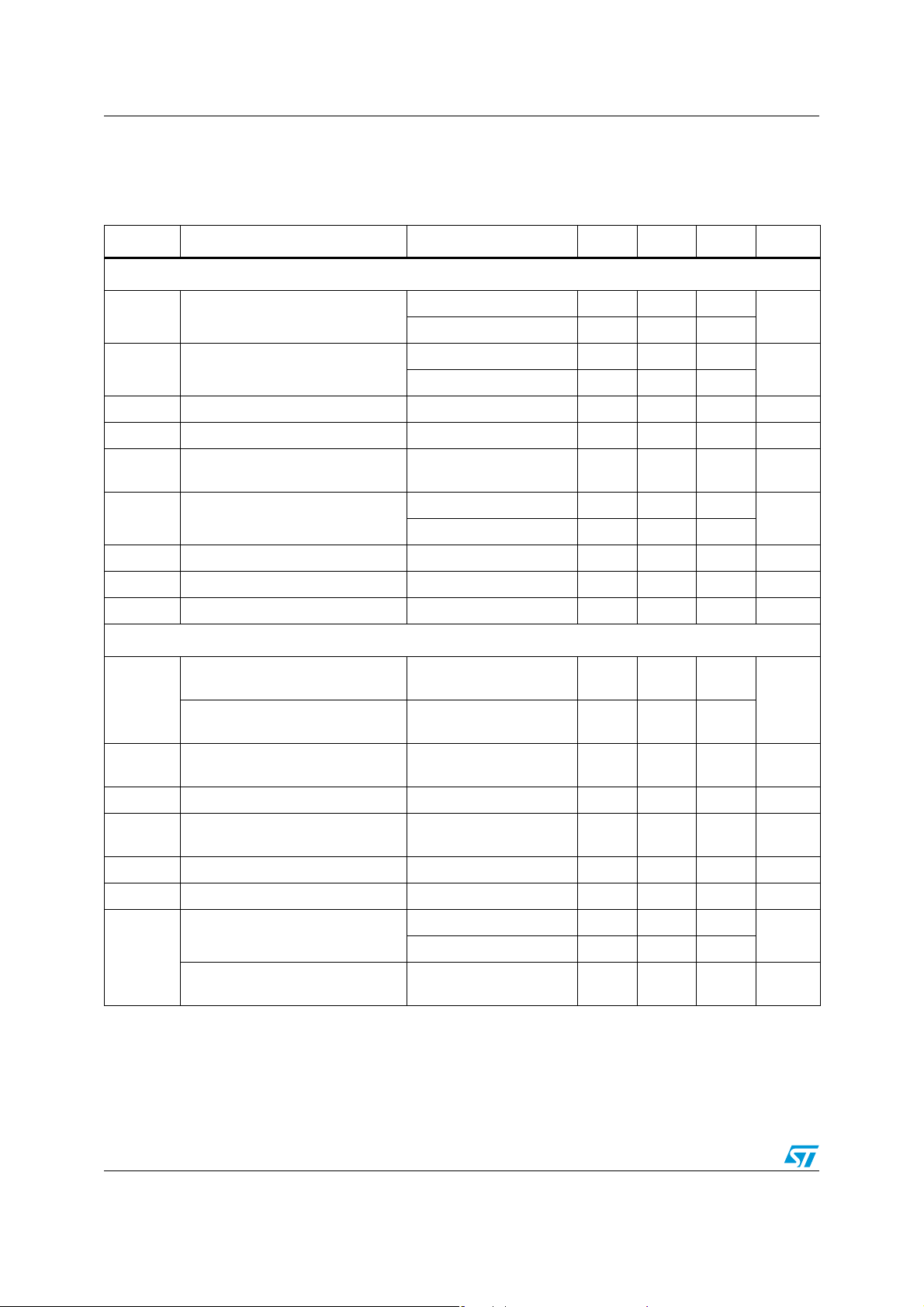
Table 3. VCC= +5V single supply, T
= 25°C (unless otherwise specified)
amb
Symbol Parameter Test conditions Min. Typ. Max. Unit
DC performance
V
OS
I
ib
R
in
C
in
PSRR
Output offset voltage
(1)
Input bias current
Input resistance T
Input capacitance T
Power supply rejection ratio
20 log (
ΔV
CC
/ΔV
out
(2)
)
No load, T
-40°C < T
T
, input to GND 5.5 16
amb
-40°C < T
amb
amb
Input to GND, F=1MHz,
ΔV
=200mV
CC
-35 -8 +35
amb
< +85°C -8.6
amb
< +85°C 6
amb
4GΩ
1pF
-90 dB
No load, input to GND 10.1 13
CC Supply current per buffer
I
G DC v oltage gain R
-40°C < T
= 150Ω, Vin=1V 1.92 2 2.05 V/V
L
< +85°C 10.3
amb
MG1 Gain matching between 3 channels Input = 1V 0.5 2 %
MG0.3 Gain matching between 3 channels Input = 0.3V 0.5 2 %
Dynamic performance and output characteristics
mV
μA
mA
-3dB bandwidth
Bw
Gain flatness @ 0.1dB
FPBW Full power bandwidth
Small signal V
V
=0.6V, RL = 150Ω
icm
Small signal V
V
=0.6V, RL = 150Ω
icm
=0.6V, V
V
icm
= 150Ω
R
L
=20mVp
out
=20mVp
out
= 2Vp-p,
out
190 340
65
130 200 MHz
D Delay between each channel 0 to 30MHz 0.5 ns
V
SR Slew rate
V
V
High level output voltage RL = 150Ω 3.7 3.9 V
OH
Low level output voltage RL = 150Ω 40 60 mV
OL
Output current
I
OUT
Output short circuit current
)
(I
source
(3)
=0.6V, V
icm
= 150Ω
R
L
= 2Vp, T
V
out
-40°C < T
= 2Vp-p,
out
amb
< +85°C 83
amb
500 740 V/μs
45 93
100 mA
MHz
mA
4/17
Page 5
TSH344 Electrical characteristics
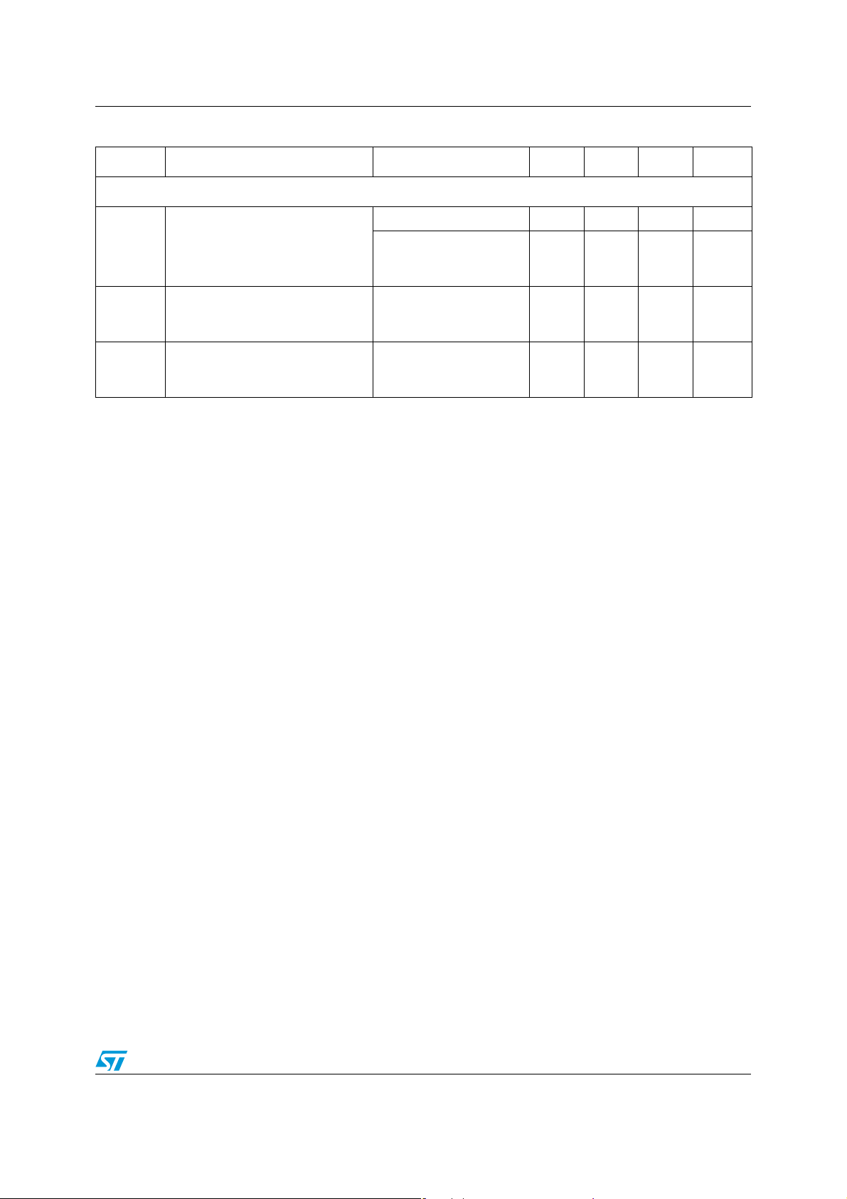
Table 3. VCC= +5V single supply, T
= 25°C (unless otherwise specified)
amb
Symbol Parameter Test conditions Min. Typ. Max. Unit
Noise and distortion
F = 100kHz, R
R
= 50Ω
eN Total input voltage noise
in
Bw=30MHz
Bw=100MHz
= 2Vp-p, RL = 150Ω
V
out
HD2 2nd harmonic distortion
F= 10MHz
F= 30MHz
V
= 2Vp-p, RL = 150Ω
HD3 3rd harmonic distortion
out
F= 10MHz
F= 30MHz
1. Output offset voltage is determined by the following expression: V
2. See Figure28 and Figure 29.
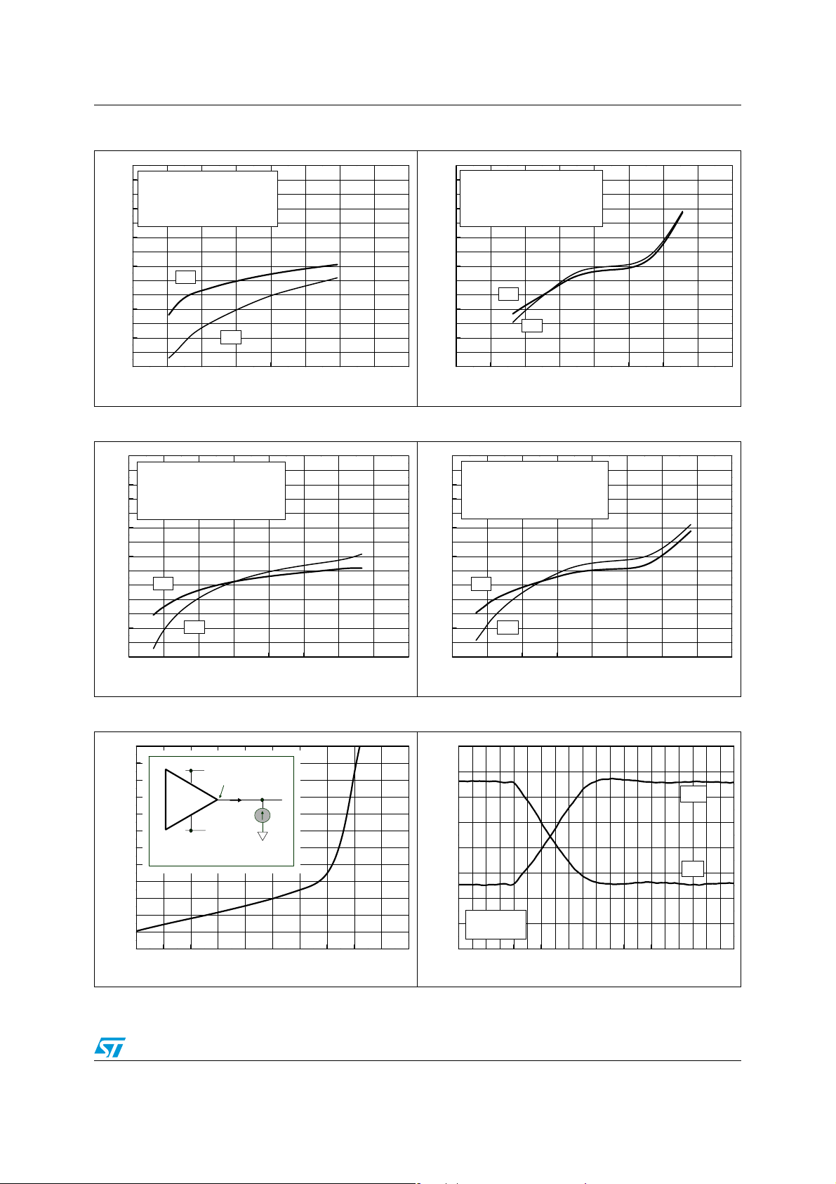
3. Non-tested value, guaranteed by design and evaluation. See Figure12.
= 50Ω 8nV/√Hz
in
55
100
-57
-42
-72
-51
=G.VIN+VOS.
OUT
μVrms
dBc
dBc
5/17
Page 6
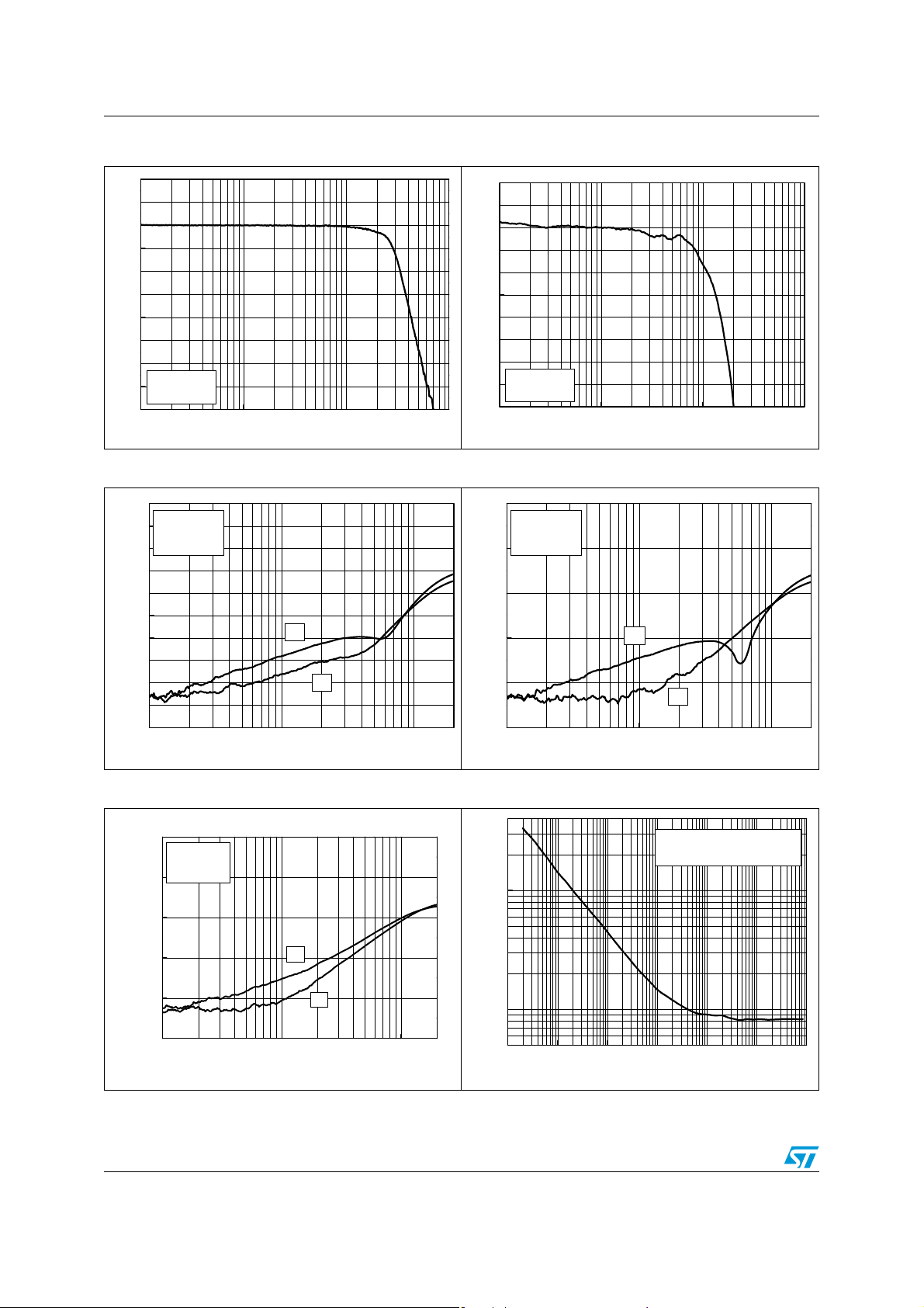
Electrical characteristics TSH344
Figure 1. Frequency response Figure 2. Gain flatness
10
8
6
4
2
0
-2
Gain (dB)
-4
-6
Vcc=5V
-8
Load=150
-10
1M 10M 100M 1G
Ω
Frequency (Hz)
6,2
6,1
6,0
5,9
5,8
5,7
5,6
Gain (dB)
5,5
5,4
Vcc=5V
5,3
Load=150
5,2
1M 10M 100M 1G
Ω
Frequency (Hz)
Figure 3. Cross-talk vs. frequency (amp1) Figure 4. Cross-talk vs. frequency (amp2)
0
Small Signal
-10
Vcc=5V
Load=150
-20
-30
-40
-50
-60
Gain (dB)
-70
-80
-90
-100
1M 10M 100M
Ω
1/2
1/3
Frequency (Hz)
0
Small Signal
Vcc=5V
Load=150
-20
-40
-60
Gain (dB)
-80
Ω
2/1
2/3
-100
1M 10M 100M
Frequency (Hz)
Figure 5. Cross-talk vs. frequency (amp3) Figure 6. Input noise vs. frequency
0
Small Signal
Vcc=5V
Load=150
-20
-40
-60
Gain (dB)
-80
-100
1M 10M 100M
Ω
3/1
3/2
Frequency (Hz)
6/17
100
Input Noise (nV/VHz)
10
10 100 1k 10k 100k 1M 10M
Frequency (Hz)
Vcc=5V
DC input = 1.5V (Battery)
Page 7
TSH344 Electrical characteristics
Figure 7. Distortion on 150Ω load - 10MHz Figure 8. Distortion on 100Ω load - 10MHz
-30
-35
-40
-45
-50
-55
-60
-65
-70
-75
-80
HD2 & HD3 (dBc)
-85
-90
-95
-100
0,0 0,5 1,0 1,5 2,0 2,5 3,0 3,5 4,0
Figure 9. Distortion on 150Ω load - 30MHz Figure 10. Distortion on 100Ω load - 30MHz
-10
-15
-20
-25
-30
-35
-40
-45
-50
-55
-60
HD2 & HD3 (dBc)
-65
-70
-75
-80
0,00,51,01,52,02,53,03,54,0
Vcc=5V
F=10MHz
input DC component = 1.15V
Load=150
Ω
HD2
HD3
Output Amplitude (Vp-p)
Vcc=5V
F=30MHz
input DC component = 1.15V
Load=150
Ω
HD2
HD3
Output Amplitude (Vp-p)
-30
-35
Vcc=5V
F=10MHz
-40
input DC component = 1.15V
-45
Load=100
-50
-55
-60
-65
-70
-75
-80
HD2 & HD3 (dBc)
-85
-90
-95
-100
0,0 0,5 1,0 1,5 2,0 2,5 3,0 3,5 4,0
Ω
HD2
HD3
Output Amplitude (Vp-p)
-10
-15
Vcc=5V
-20
F=30MHz
input DC component = 1.15V
-25
Load=100
-30
-35
-40
-45
-50
HD2
-55
-60
HD2 & HD3 (dBc)
-65
-70
-75
-80
0,00,51,01,52,02,53,03,54,0
Ω
HD3
Output Amplitude (Vp-p)
Figure 11. Output current Figure 12. Slew rate
0
-10
-20
-30
-40
-50
-60
-70
Isource (mA)
-80
-90
-100
-110
-120
0,0 0,5 1,0 1,5 2,0 2,5 3,0 3,5 4,0 4,5 5,0
+5V
VOH
without load
Isource
0V
V
V (V)
4,0
3,5
3,0
2,5
2,0
1,5
1,0
Output Response (V)
Vcc=5V
0,5
Load=150
0,0
-2-1012345678
Ω
7/17
SR+
SR-
Time (ns)
Page 8
Electrical characteristics TSH344
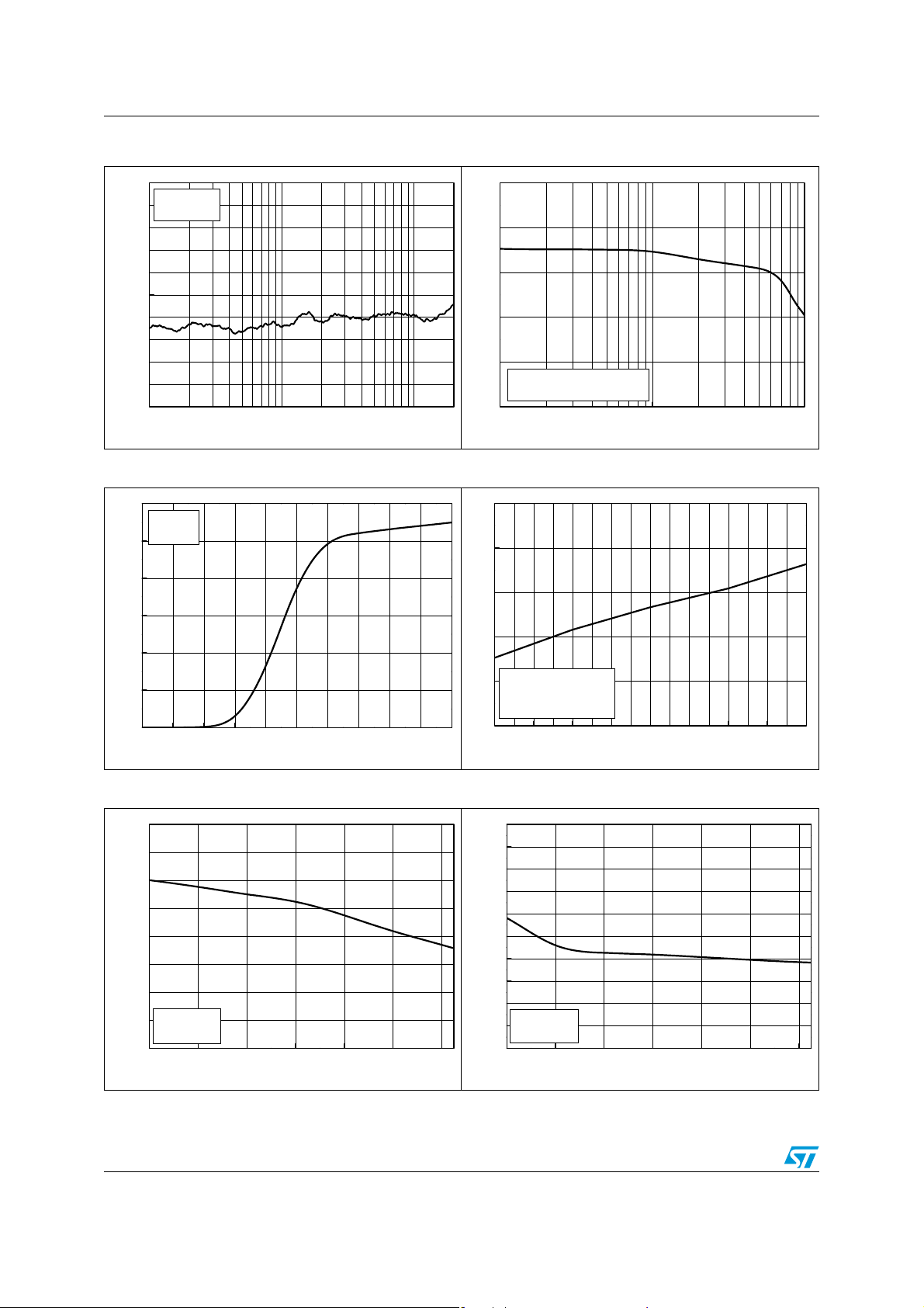
Figure 13. Reverse isolation vs. frequency Figure 14. Output swing vs. frequency
0
Vcc=5V
-10
Load=150
-20
-30
-40
-50
-60
Gain (dB)
-70
-80
-90
-100
1M 10M 100M
Ω
Frequency (Hz)
Figure 15. Quiescent current vs. supply Figure 16. Output swing vs. supply
30
Vcc=5V
no load
25
20
15
10
Total Icc (mA)
5
0
0,0 0,5 1,0 1,5 2,0 2,5 3,0 3,5 4,0 4,5 5,0
Vcc (V)
5
4
3
2
Vout max. (Vp-p)
1
Vcc=5V
Load=100
0
1M 10M 100M
Ω or Load=150Ω
Frequency (Hz)
5
4
3
2
Vout peak-peak (Vp-p)
1
Vcc=5V
F=30MHz
Load=100
0
3,00 3,25 3,50 3,75 4,00 4,25 4,50 4,75 5,00
Ω or 150Ω
Vcc (V)
Figure 17. Bandwidth vs. temperature Figure 18. Voltage gain vs. temperature
500
450
400
350
300
Bw (MHz)
250
200
150
Vcc=5V
Load=150
100
-40-200 20406080
Ω
Temperature (°C)
8/17
2,05
2,04
2,03
2,02
2,01
2,00
1,99
Gain (dB)
1,98
1,97
Vcc=5V
1,96
Load=150
1,95
-40-200 20406080
Ω
Temperature (°C)
Page 9
TSH344 Electrical characteristics
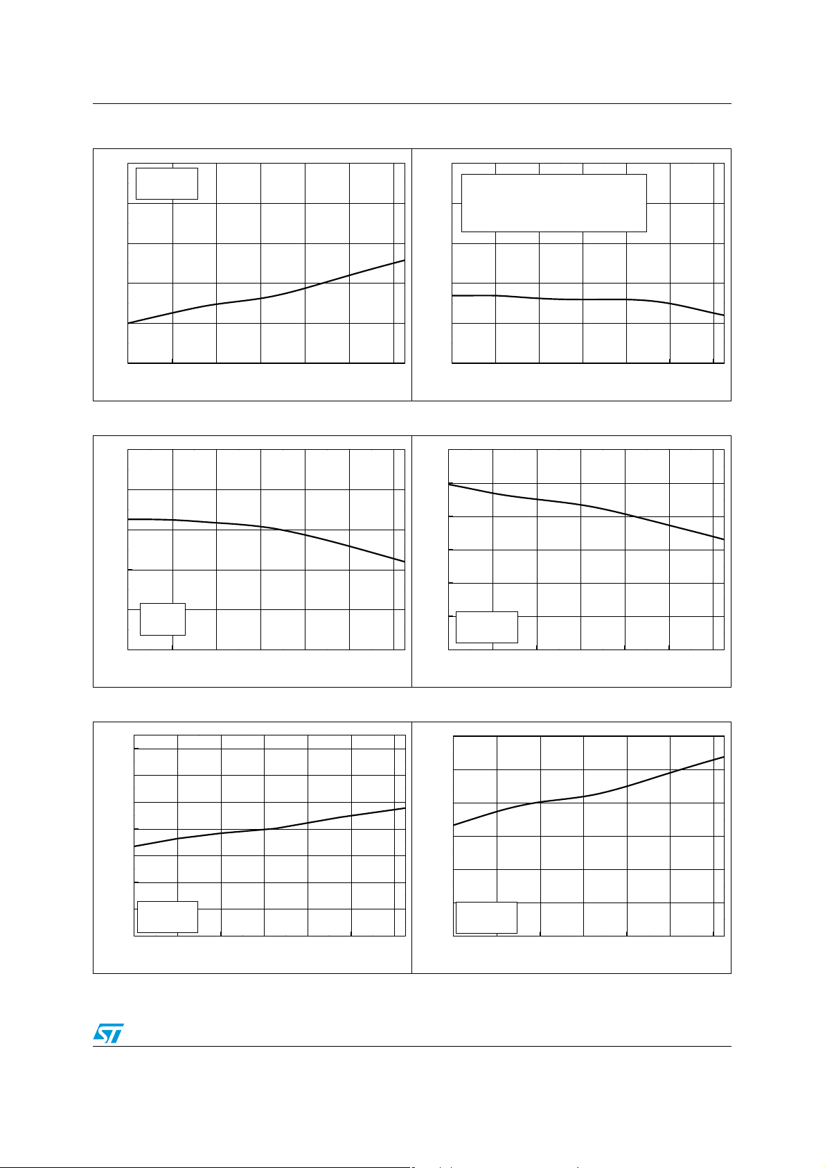
Figure 19. I
2
3
Vcc=5V
Load=150
vs. temperature Figure 20. Gain matching vs. temperature
bias
1,0
Ω
Gain Matching between 3 channels
Vcc=5V
0,8
Load=150
Ω
Vin=0.3V and 1V
4
0,6
(μA)
BIAS
5
I
6
7
-40 -20 0 20 40 60 80
Temperature (°C)
GM (%)
0,4
0,2
0,0
-40-200 20406080
Temperature (°C)
Figure 21. Supply current vs. temperature Figure 22. Output current vs. temperature
12
11
10
(mA)
CC
I
9
110
100
90
80
70
Isource (mA)
8
Vcc=5V
no Load
7
-40 -20 0 20 40 60 80
Temperature (°C)
60
Vcc=5V
Load=150
50
-40-200 20406080
Ω
Temperature (°C)
Figure 23. Output higher rail vs. temperature Figure 24. Output lower rail vs. temperature
4,2
4,1
4,0
3,9
(V)
OH
V
3,8
3,7
3,6
Vcc=5V
Load=150
3,5
-40 -20 0 20 40 60 80
Ω
Temperature (°C)
50
45
40
35
(V)
OL
V
30
25
Vcc=5V
Load=150
20
-40 -20 0 20 40 60 80
Ω
Temperature (°C)
9/17
Page 10
Application information TSH344
3 Application information
3.1 Using the TSH344 to drive R-G-B video components
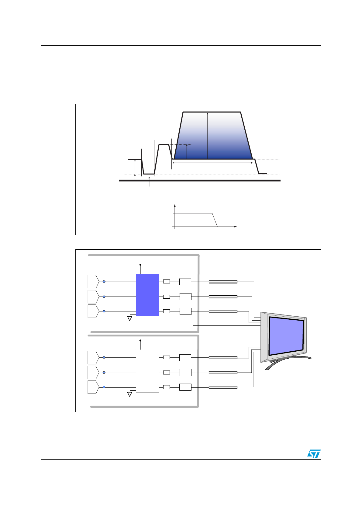
Figure 25. Shapes of video signals coming from DACs
GND
300mV
10mV
54ns
(4t)
27ns
(2t)
590ns
590ns
(44t)
Synchronization tip
27ns
(2t)
(44t)
Amplitude
1Vp-p
300mV
700mV
14.8µs (1100t): 1920*1080i
24.3µs (1800t): 1280*720i
White (100 IRE)
•Fclock=74.25MHz
•t=1/Fclock=13.5ns
Black (30 IRE)
(0 IRE)
1.030V
0.330V
0.030V
time
Figure 26. TSH344 in single supply for HD
video
outputs
DAC
DAC
DAC
video
outputs
DAC
DAC
DAC
R
G
B
Y,G(+synchro)
Pb,B
Pr,R
+5V
TSH344
SO8
+5V
TSH343
SO8
75Ω
LPF
75Ω
LPF
75Ω
LPF
Digital synchro
75Ω
LPF
75Ω
LPF
75Ω
LPF
30MHz
Frequency
Cable
Cable
Cable
HDTV
Cable
Cable
Cable
Note: Se e the TSH343 datasheet on st.com for more information (the TSH343 is used to drive a
video signal including a synchronization tip).
10/17
Page 11
TSH344 Application information
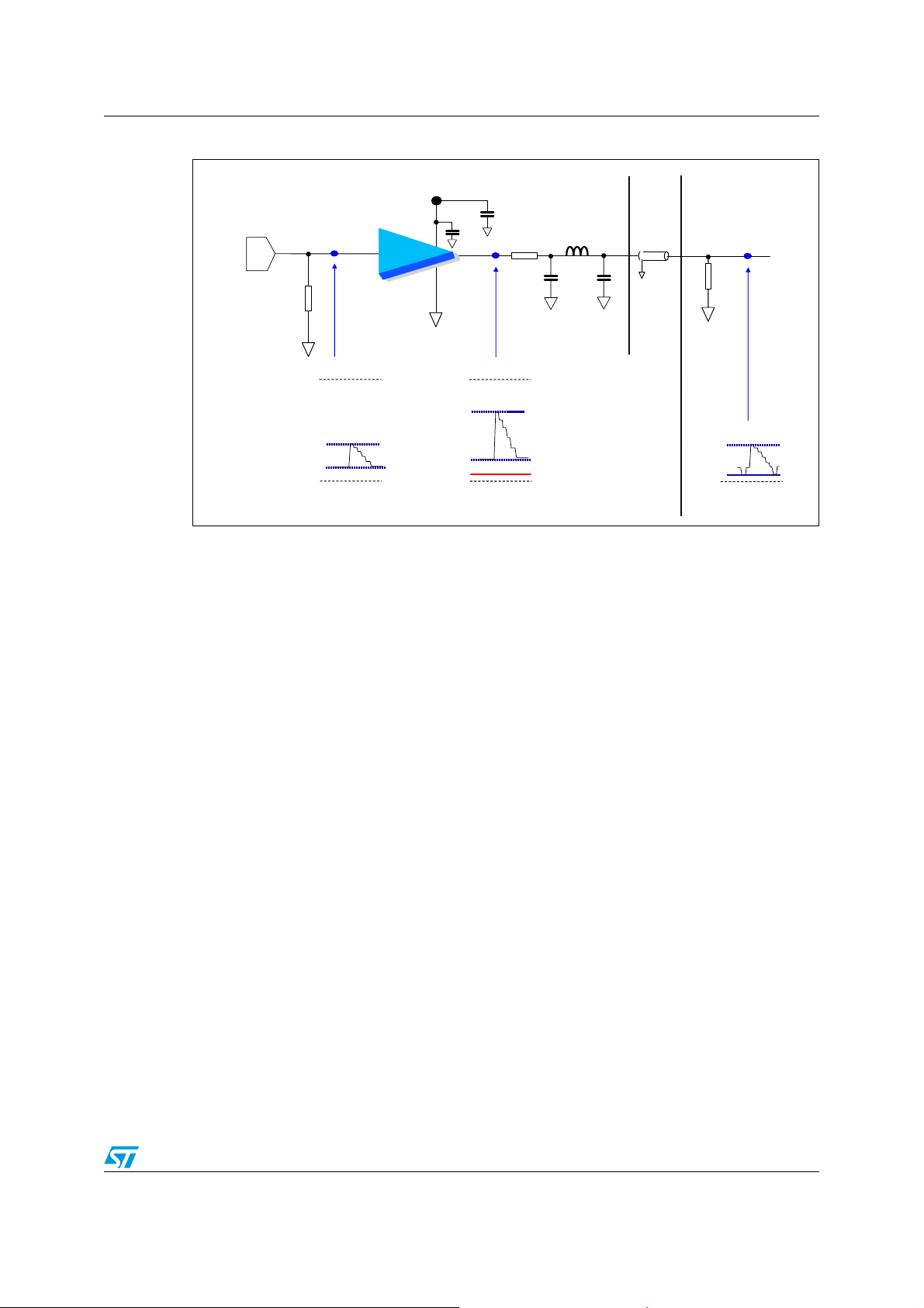
Figure 27. Details on one channel of the TSH344
DAC
External resistor.
Load required by
the DAC output
specification
300mV
1V
5Volt
0Volt
1/3 TSH344
(gain=2)
+5V
600mV
0V
2V
10nF
5Volt
0Volt
+
100µF
75Ω
Low output Rail :
60mV max. tested
(see datasheet p.3: Vol)
68pF
470nH
STB
video line
68pF
TV
75Ω
1V
300mV
0Volt
Because of the shape of the signal described in Figure 25, we use a very low output rail
triple high-speed buffer. The TSH344 supplied in 5V single power supply features a low
output rail of 60mV (guaranteed by test) on 150Ω load. It is dedicated for driving RGB
signals without synchronisation (in the case where the synchronization is provided digitally
on the digital bus).
The gain of the TSH344 (gain=2) is internal which make s it possib le to remo v e tw o resist ors
on the BOM. To avoid any perturbation on matching from the DACs output impedance along
a large band of 30MHz in HD, a discrete reconstruction filtering is implemented after the
driver. This filter is matched on 75Ω. Note that the TSH344 uses a single supply architecture
and it is not AC o utput coupled (it ca nnot sink an output curre nt, theref ore it is not possible to
implement an output series capacitor).
11/17
Page 12
Application information TSH344
3.2 Power supply considerations
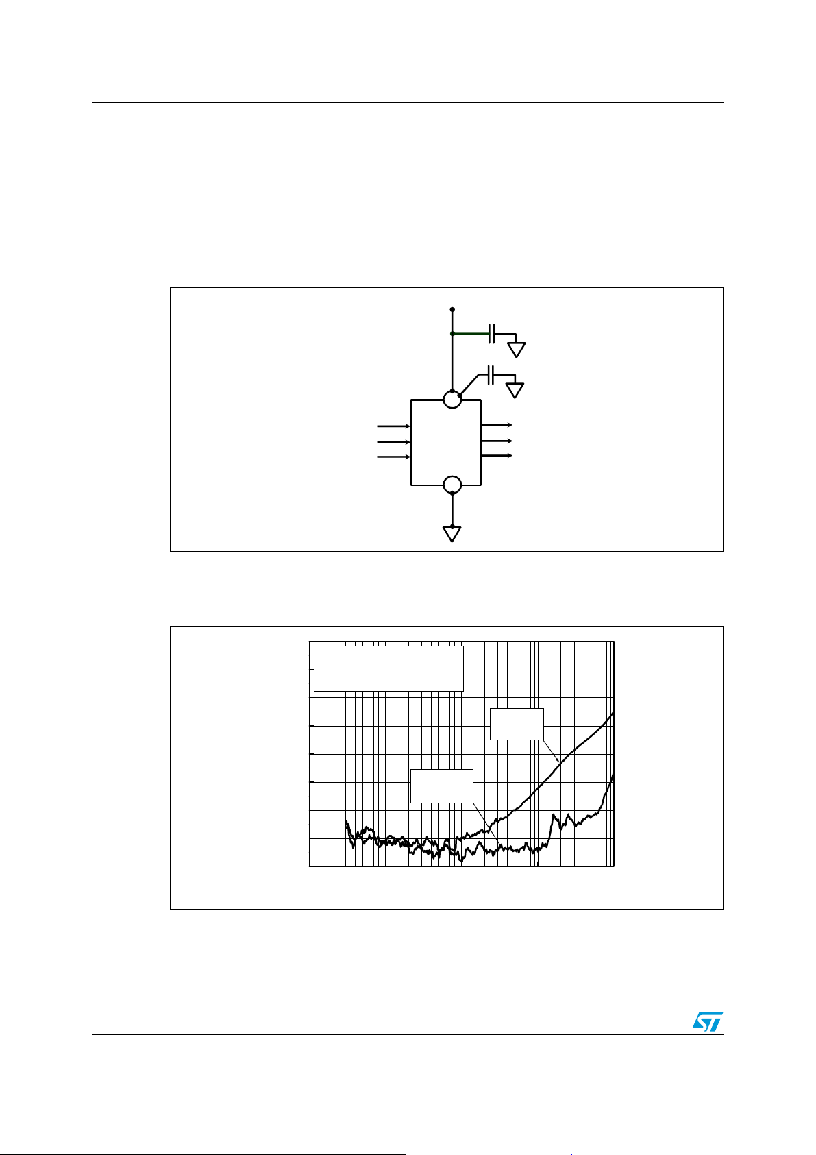
Correct power supply bypassing is very important for optimizing performance in low and
high-frequency ranges. Bypass capacitors should be placed as close as possible to the IC
pin (pin 4) to improve high-frequency bypassing. A capacitor (C
necessary to improve the PSRR in low frequencies. F or better quality bypassing, a capacitor
of 470nF (C
) is also added as close as possible to the IC pin to improve the PSRR in the
HF
higher frequencies.
Figure 28. Circuit for power supply bypassing
+VCC
C
LF
+
C
HF
4
R
G
TSH344
B
5
) greater than 100μF is
LF
Figure 29 shows how the power supply noise rejection evolves versus frequen cy depending
on how carefully the power supply decoupling is achi eved.
Figure 29. Improvement of power supply nois e rejection
0
Vcc=5V
-10
Load=150
PSRR=20 log (ΔVCC/ΔVout)
-20
-30
-40
-50
PSRR (dB)
-60
-70
-80
10k 100k 1M 10M 100M
Ω
without
capacitor
CLF=100uF
C
=470nF
HF
Frequency (Hz)
12/17
Page 13
TSH344 Application information
3.3 Delay between channels
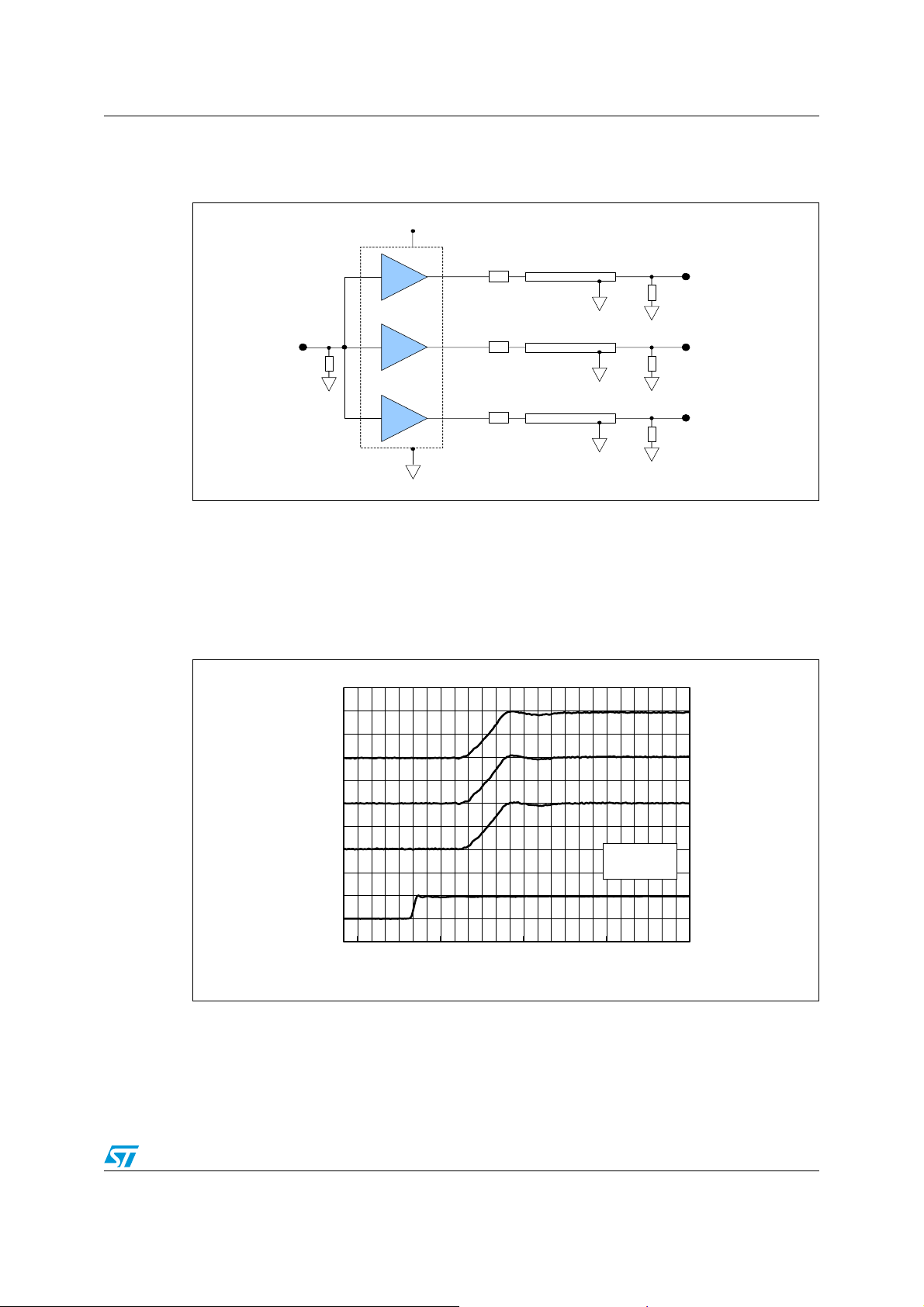
Figure 30. Measurement of the delay between each channel
5V
Vin
75Ω
+6dB
75Ω
75Ω
+6dB
75Ω
+6dB
75Ω Cable
75Ω Cable
75Ω Cable
V1
75Ω
V2
75Ω
V3
75Ω
The delay between each video component is an important aspect in high definition video
systems. To properly drive the three video components without any relative de la y, the layout
of the TSH344 dice has a very symmetrical geometry. this has a direct effect on the
synchronization of each channel, as shown in Figure 31. There is no delay detected
between channels when the same V
signal is applied on the three inputs. Note that the
in
delay between the inputs and the outputs is equal to 4ns.
Figure 31. Relative delay between each channel
Vcc=5V
Load=150
Input 3 Output responses
-4ns -2ns 0s 2ns 4ns 6ns 8ns 10ns 12ns 14ns 16ns 18ns 20ns
Time
13/17
Ω
Page 14

Package information TSH344
4 Package information
In order to meet environmental requirements, STMicroelectronics offers these devices in
ECOPACK
category of second level interconnect is marke d on the pa ckage and on the inner box label,
in compliance with JEDEC Standard JESD97. The maximum ratings related t o soldering
conditions are also marked on the inner box label. ECOPACK is an STMicroelectronics
trademark. ECOPACK specifications are available at: www.st.com
®
packages. These packages have a lead-free second level interconnect. The
.
14/17
Page 15
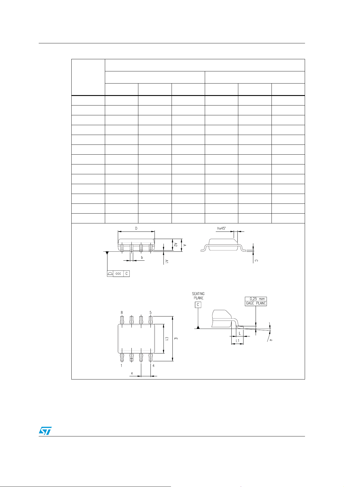
TSH344 Package information
Figure 32. SO-8 package mechanical data
Dimensions
Ref.
Min. Typ. Max. Min. Typ. Max.
A1.750.069
A1 0.10 0.25 0.004 0.010
A2 1.25 0.049
b 0.28 0.48 0.011 0.019
c 0.17 0.23 0.007 0.010
D 4.804.905.000.1890.1930.197
E 5.806.006.200.2280.2360.244
E1 3.80 3.90 4.00 0.150 0.154 0.157
e 1.27 0.050
h 0.25 0.50 0.010 0.020
L 0.40 1.27 0.016 0.050
k1°8°1°8°
ccc 0.10 0.004
Millimeters Inches
15/17
Page 16
Ordering information TSH344
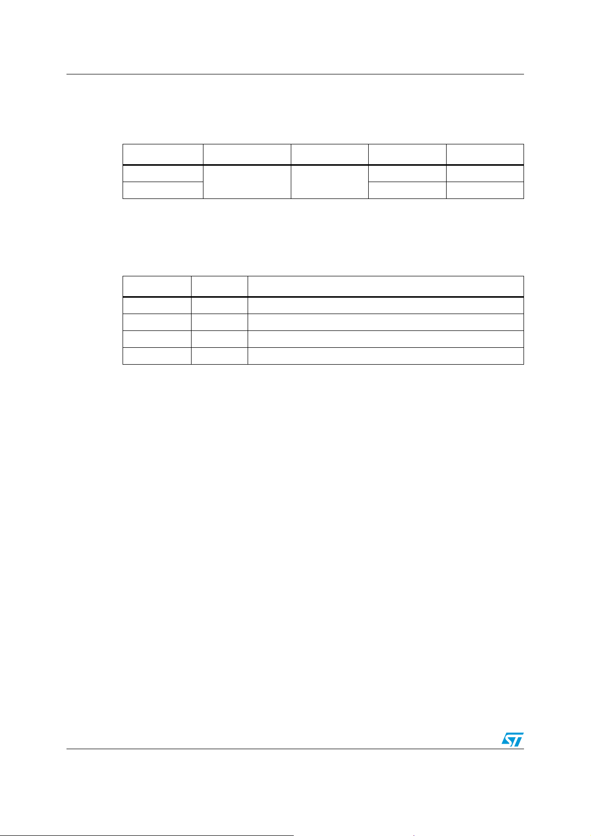
5 Ordering information
Table 4. Order codes
Part number Temperature range Package Packing Marking
TSH344ID
-40°C to +85°C SO-8
TSH344IDT Tape & reel TSH344I
6 Revision history
Date Revision Changes
Dec-2005 1 First release of datasheet.
Jan-2006 2 Capa-load option paragraph deleted on page 11.
Jul-2006 3 Application information.
14-Mar-2007 4 Updated
Tube TSH344I
Section 3.2: Power supply considerations on page 12 .
16/17
Page 17

TSH344
Please Read Carefully:
Information in this document is provided solely in connection with ST products. STMicroelectronics NV and its subsidiaries (“ST”) reserve the
right to make changes, corrections, modifications or improvements, to this document, and the products and services described herein at any
time, without notice.
All ST products are sold pursuant to ST’s terms and conditions of sale.
Purchasers are solely res ponsibl e fo r the c hoic e, se lecti on an d use o f the S T prod ucts and s ervi ces d escr ibed he rein , and ST as sumes no
liability whatsoever relati ng to the choice, selection or use o f the ST products and services desc ribed herein.
No license, express or implied, by estoppel or otherwise, to any intellectual property rights is granted under this document. If any part of this
document refers to any third pa rty p ro duc ts or se rv ices it sh all n ot be deem ed a lice ns e gr ant by ST fo r t he use of su ch thi r d party products
or services, or any intellectua l property c ontained the rein or consi dered as a warr anty coverin g the use in any manner whats oever of suc h
third party products or servi ces or any intellectual property contained therein.
UNLESS OTHERWISE SET FORTH IN ST’S TERMS AND CONDITIONS OF SALE ST DISCLAIMS ANY EXPRESS OR IMPLIED
WARRANTY WITH RESPECT TO THE USE AND/OR SALE OF ST PRODUCTS INCLUDING WITHOUT LIMITATION IMPLIED
WARRANTIES OF MERCHANTABILITY, FITNESS FOR A PARTICUL AR PURPOS E (AND THEIR EQUIVALE NTS UNDER THE LAWS
OF ANY JURISDICTION), OR INFRINGEMENT OF ANY PATENT, COPYRIGHT OR OTHER INTELLECTUAL PROPERTY RIGHT.
UNLESS EXPRESSLY APPROVED IN WRITING BY AN AUTHORIZED ST REPRESENTATIVE, ST PRODUCTS ARE NOT
RECOMMENDED, AUTHORIZED OR WARRANTED FOR USE IN MILITARY, AIR CRAFT, SPACE, LIFE SAVING, OR LIFE SUSTAINING
APPLICATIONS, NOR IN PRODUCTS OR SYSTEMS WHERE FAILURE OR MALFUNCTION MAY RESULT IN PERSONAL INJ URY,
DEATH, OR SEVERE PROPERTY OR ENVIRONMENTAL DAMAGE. ST PRODUCTS WHICH ARE NOT SPECIFIED AS "AUTOMOTIVE
GRADE" MAY ONLY BE USED IN AUTOMOTIVE APPLICATIONS AT USER’S OWN RISK.
Resale of ST products with provisions different from the statements and/or technical features set forth in this document shall immediately void
any warranty granted by ST fo r the ST pro duct or serv ice describe d herein and shall not cr eate or exten d in any manne r whatsoever , any
liability of ST.
ST and the ST logo are trademarks or registered trademarks of ST in various countries.
Information in this document su persedes and replaces all information previously supplied.
The ST logo is a registered trademark of STMicroelectronics. All other names are the property of their respective owners.
© 2007 STMicroelectronics - All rights reserved
STMicroelectronics group of compan ie s
Australia - Belgium - Brazil - Canada - China - Czech Republic - Finland - France - Germany - Hong Kong - India - Israel - Italy - Japan -
Malaysia - Malta - Morocco - Singapore - Spain - Sweden - Switzerland - United Kingdom - United States of America
www.st.com
17/17
 Loading...