

Page 1

High-voltage, high-side current sense amplifier
t
Features
■ Independent supply and input common-mode
voltages
■ Wide common-mode operating range:
2.9 to 70 V in single-supply configuration
-2.1 to 65 V in dual-supply configuration
■ Wide common-mode surviving range:
-16 to 75 V (reversed battery and load-dump
conditions)
■ Supply voltage range:
2.7 to 5.5 V in single supply configuration
■ Low current consumption: I
■ Pin selectable gain: 50 V/V or 100 V/V
■ Buffered output
■ EMI filtering
Applications
■ Automotive current monitoring
■ DC motor control
■ Photovoltaic systems
■ Battery chargers
■ Precision current sources
■ Current monitoring of notebook computers
■ Uninterruptible power supplies
■ High-end power supplies
Description
The TSC1031 measures a small differential
voltage on a high-side shunt resistor and
translates it into a ground-referenced output
voltage. The TSC1031’s dedicated schematic
eases the implementation of EMI filtering in harsh
environments. The gain is adjustable to 50 V/V or
100 V/V by a selection pin.
max = 360 µA
CC
TSC1031
TSSOP8
(Plastic package)
SO-8
(Plastic package)
Vm
1
A1
2
SEL
3
Ou
4
Pin connections
(top view)
Wide input common-mode voltage range, low
quiescent current, and tiny TSSOP8 packaging
enable use in a wide variety of applications.
The input common-mode and power supply
voltages are independent. The common-mode
voltage can range from 2.9 to 70 V in the singlesupply configuration or be offset by an adjustable
voltage supplied on the Vcc- pin in the dualsupply configuration.
With a current consumption lower than 360 µA
and a virtually null input leakage current in
standby mode, the power consumption in the
applications is minimized.
Vp
8
Vcc-
7
Gnd
6
Vcc+
5
April 2011 Doc ID 16875 Rev 2 1/26
www.st.com
26
Page 2

Contents TSC1031
Contents
1 Application schematic and pin description . . . . . . . . . . . . . . . . . . . . . . 3
2 Absolute maximum ratings and operating conditions . . . . . . . . . . . . . 6
3 Electrical characteristics . . . . . . . . . . . . . . . . . . . . . . . . . . . . . . . . . . . . . 7
4 Electrical characteristics curves: current sense amplifier . . . . . . . . . 10
5 Parameter definitions . . . . . . . . . . . . . . . . . . . . . . . . . . . . . . . . . . . . . . . 13
5.1 Common mode rejection ratio (CMR) . . . . . . . . . . . . . . . . . . . . . . . . . . . . 13
5.2 Supply voltage rejection ratio (SVR) . . . . . . . . . . . . . . . . . . . . . . . . . . . . 13
5.3 Gain (Av) and input offset voltage (V
5.4 Output voltage drift versus temperature . . . . . . . . . . . . . . . . . . . . . . . . . . 15
5.5 Input offset drift versus temperature . . . . . . . . . . . . . . . . . . . . . . . . . . . . . 16
5.6 Output voltage accuracy . . . . . . . . . . . . . . . . . . . . . . . . . . . . . . . . . . . . . . 16
) . . . . . . . . . . . . . . . . . . . . . . . . . . 13
os
6 Maximum permissible voltages on pins . . . . . . . . . . . . . . . . . . . . . . . . 18
7 Application information . . . . . . . . . . . . . . . . . . . . . . . . . . . . . . . . . . . . . 19
8 Package information . . . . . . . . . . . . . . . . . . . . . . . . . . . . . . . . . . . . . . . . 21
8.1 SO-8 package information . . . . . . . . . . . . . . . . . . . . . . . . . . . . . . . . . . . . 22
8.2 TSSOP-8 package information . . . . . . . . . . . . . . . . . . . . . . . . . . . . . . . . . 23
9 Ordering information . . . . . . . . . . . . . . . . . . . . . . . . . . . . . . . . . . . . . . . 24
10 Revision history . . . . . . . . . . . . . . . . . . . . . . . . . . . . . . . . . . . . . . . . . . . 25
2/26 Doc ID 16875 Rev 2
Page 3

TSC1031 Application schematic and pin description
1 Application schematic and pin description
The TSC1031 high-side current sense amplifier can be used in either single- or dual-supply
mode. In the single-supply configuration, the TSC1031 features a wide 2.9 V to 70 V input
common-mode range totally independent of the supply voltage. In the dual-supply range,
the common-mode range is shifted by the value of the negative voltage applied on the Vccpin. For instance, with Vcc+ = 5 V and Vcc- = -5 V, then the input common-mode range is
-2.1 V to 65 V.
Figure 1. Single-supply configuration schematic
Vsense
Iload
Common-mode voltage: 2.9 V to 70 V
Rf1
Cf
Vp Vm
Rg1
TSC1031
Rf2
Rg2
Cf
Sense
amplifier
Rg3
A1
Rf3
Vcc
Vol tage
buffer
K2
SEL
Out
5 V
Vcc
GPIO
ADC
GndGndVcc-
µController
AM04523
Doc ID 16875 Rev 2 3/26
Page 4

Application schematic and pin description TSC1031
Figure 2. Dual-supply configuration schematic
Vsense
Rf1
Cf
Rf2
Iload
Cf
Common-mode voltage: -2.1 V to 65 V
5 V
Vp Vm
Rg1
Rg2
TSC1031
Sense
amplifier
Rg3
A1
Rf3
Vcc
Vol tage
buffer
K2
GndVcc-
SEL
Out
Vcc
GPIO
ADC
Gnd
µController
-5 V
AM04524
4/26 Doc ID 16875 Rev 2
Page 5

TSC1031 Application schematic and pin description
Figure 3. Common-mode versus supply voltage in dual-supply configuration
Vicm
common-mode voltage
operating range
Max = 70 V
min = 2.9 V
V
= 0 V V
cc-
Max = 65 V
min = -2.1 V
= -5 V
cc-
Max = 60 V
min = -7.1 V
V
= -10 V
cc-
Single-supply Dual-supply
AM04519
Ta bl e 1 describes the function of each pin. Their position is shown in the illustration on the
cover page and in Figure 1 on page 3.
Table 1. Pin description
Symbol Type Function
Out Analog output
Gnd Power supply Ground line.
Vcc+ Power supply Positive power supply line.
Vcc- Power supply Negative power supply line.
Vp Analog input
Vm Analog input
SEL Digital input Gain-select pin.
A1 Analog output Connection to the output resistor.
The Out voltage is proportional to the magnitude of the sense
voltage V
p-Vm
.
Connection for the external sense resistor. The measured current
enters the shunt on the V
side.
p
Connection for the external sense resistor. The measured current
exits the shunt on the V
side.
m
Doc ID 16875 Rev 2 5/26
Page 6

Absolute maximum ratings and operating conditions TSC1031
2 Absolute maximum ratings and operating conditions
Table 2. Absolute maximum ratings
Symbol Parameter Value Unit
V
V
in_sense
V
in_sel
V
in_A1
V
cc+
V
cc+-Vcc-
V
out
T
stg
T
id
Input pins differential voltage (Vp-Vm)±20V
Sensing pins input voltages (Vp, Vm)
Gain selection pin input voltage (SEL)
A1 pin input voltage
Positive supply voltage
(2)
(2)
(1)
(2)
-16 to 75 V
-0.3 to V
-0.3 to V
+0.3 V
cc+
+0.3 V
cc+
-0.3 to 7 V
DC supply voltage 0 to 15 V
DC output pin voltage
(2)
-0.3 to V
+0.3 V
cc+
Storage temperature -55 to 150 °C
Maximum junction temperature 150 °C
j
TSSOP8 thermal resistance junction to ambient 120 °C/W
R
thja
ESD
1. These voltage values are measured with respect to the V
2. These voltage values are measured with respect to the Gnd pin.
3. Human body model: a 100 pF capacitor is charged to the specified voltage, then discharged through a
1.5 kΩ resistor between two pins of the device. This is done for all couples of connected pin combinations
while the other pins are floating.
4. Machine model: a 200 pF capacitor is charged to the specified voltage, then discharged directly between
two pins of the device with no external series resistor (internal resistor < 5 Ω). This is done for all couples of
connected pin combinations while the other pins are floating.
5. Charged device model: all pins plus package are charged together to the specified voltage and then
discharged directly to ground.
Table 3. Operating conditions
SO-8 thermal resistance junction to ambient 125 °C/W
HBM: human body model
MM: machine model
(3)
(4)
CDM: charged device model
(5)
cc-
pin.
2.5 kV
150 V
1.5 kV
Symbol Parameter Value Unit
DC supply voltage in single-supply configuration
V
cc+
from T
(V
to T
min
connected to Gnd = 0 V)
cc-
max
Negative supply voltage in dual-supply
V
V
T
cc-
icm
oper
configuration from T
V
= 5.5 V max -8 to 0 V
cc+
= 3 V max -11 to 0 V
V
cc+
Common-mode voltage range referred to pin Vcc (T
min
to T
max
)
Operational temperature range (T
min
to T
max
min
to T
6/26 Doc ID 16875 Rev 2
2.7 to 5.5 V
2.9 to 70 V
) -40 to 125 °C
max
Page 7

TSC1031 Electrical characteristics
3 Electrical characteristics
The electrical characteristics given in the following tables are measured under the following
test conditions unless otherwise specified.
● T
● V
● Rf1, Rf2 and Rf3 resistors are short-circuited.
Table 4. Supply
Symbol Parameter Test conditions Min. Typ. Max. Unit
=25°C, V
amb
sense=Vp-Vm
cc+
=5V, V
connected to Gnd (single-supply configuration).
cc-
=50mV, Vm= 12 V, no load on Out, all gain configurations.
I
I
CC1
Table 5. Input
Total supply current V
CC
Total supply current
= 0 V, T
sense
= 50 mV Av = 50 V/V
V
sense
< T
T
min
amb
< T
min
max
< T
amb
< T
max
200 360 µA
300 480 µA
Symbol Parameter Test conditions Min. Typ. Max. Unit
DC common-mode rejection
DC CMR
Variation of V
out
referred to input
versus V
(1)
2.9 V< Vm < 70 V, T
icm
min
< T
amb
< T
90 105 dB
max
AC common-mode rejection
AC CMR
Variation of V
versus V
out
referred to input (peak-to-peak
Av = 50 V/V or 100 V/V
icm
2.9 V< V
< 30 V, 1 kHz sine wave
icm
95 dB
voltage variation)
Supply voltage rejection
Variation of V
Input offset voltage
os
/dT Input offset drift vs. T
I
Input leakage current
lk
I
Input bias current
ib
dV
SVR
V
os
versus V
out
(3)
Av = 50 V/V, 2.7 V< VCC < 5.5 V
(2)
V
=30mV, T
T
T
amb
sense
< T
min
=25°C
amb
< T
max
CC
Av = 50 V/V
T
< T
amb
=0V
< T
amb
=0V
< T
amb
< T
< T
< T
max
max
max
V
T
V
T
min
CC
min
sense
min
min
< T
amb
< T
max
85 100 dB
±500
±1100
-20 +5 µV/°C
1µA
10 15 µA
Rg Input resistor value Valid for Rg1 and Rg2 5 kΩ
V
< VCC < V
min
V
V
I
1. See Chapter 5: Parameter definitions on page 13 for the definition of CMR.
2. See Chapter 5 for the definition of SVR.
3. See Chapter 5 for the definition of V
Logic low voltage (SEL)
IL
Logic high voltage (SEL)
IH
Gain-select pins (SEL)
sel
leakage input current
.
os
CC
T
< T
amb
< VCC < V
min
< T
amb
< T
< T
min
V
CC
T
min
SEL pin connected to GND or V
T
< T
amb
< T
min
max
max
max
CC
CC
max
max
CC
-0.3 0.5 V
1.2 V
CC
400 nA
µV
V
Doc ID 16875 Rev 2 7/26
Page 8

Electrical characteristics TSC1031
Table 6. Output
Symbol Parameter Test conditions Min. Typ. Max. Unit
K1
K2 Current multiplier gain
Av Total gain (Av = 2.K1.K2)
ΔV
out
ΔV
out
ΔV
ΔV
ΔV
ΔV
ΔV
I
sc
V
OH
V
1. See Chapter 5: Parameter definitions on page 13 for the definition of output voltage drift versus temperature.
2. The output voltage accuracy is the difference with the expected theoretical output voltage V
for a more detailed definition.
Except for Av = 100 V/V.
3.
Sense amplifier gain
(K1 = Rg3/Rg1)
/ΔT Output voltage drift vs. T
/ΔI
Output stage load regulation
out
Total output voltage accuracy
out
Total output voltage accuracy
out
Total output voltage accuracy
out
Total output voltage accuracy
out
Total output voltage accuracy
out
Short-circuit current
Output stage high-state saturation
voltage
V
OH=VCC-Vout
Output stage low-state saturation
OL
voltage
(1)
SEL= Gnd
SEL= Vcc+
SEL= Gnd
SEL= Vcc+
Av = 50 V/V
T
min
-10 mA < I
sink or source current
I
out
Av = 50 V/V, T
V
(2)
sense
T
amb
T
min
V
sense
T
amb
T
min
V
sense
T
min
V
sense
T
min
V
sense
T
min
OUT connected to V
GND
V
sense
I
out
V
sense
I
out
< T
amb
=50mV
=25°C
< T
amb
=90mV
=25°C
< T
amb
=20mV T
< T
amb
=10mV T
< T
amb
=5mV T
< T
amb
=1V
=1mA
=-1V
=1mA
< T
out
< T
< T
< T
< T
< T
max
<10 mA
= 25° C
amb
(3)
max
(3)
max
amb
max
amb
max
amb
max
=25° C
=25° C
=25°C
or
CC
10
2.5
5
50
100
±240 ppm/°C
0.3 ±1.5 mV/mA
±2.5
±4
±3.5
±5
±3.5
±5
±5.5
±8
±10
±22
15 26 mA
85 135 mV
80 125 mV
out-th
=Av*V
. See Chapter 5
sense
V/V
%
%
%
%
%
8/26 Doc ID 16875 Rev 2
Page 9
TSC1031 Electrical characteristics
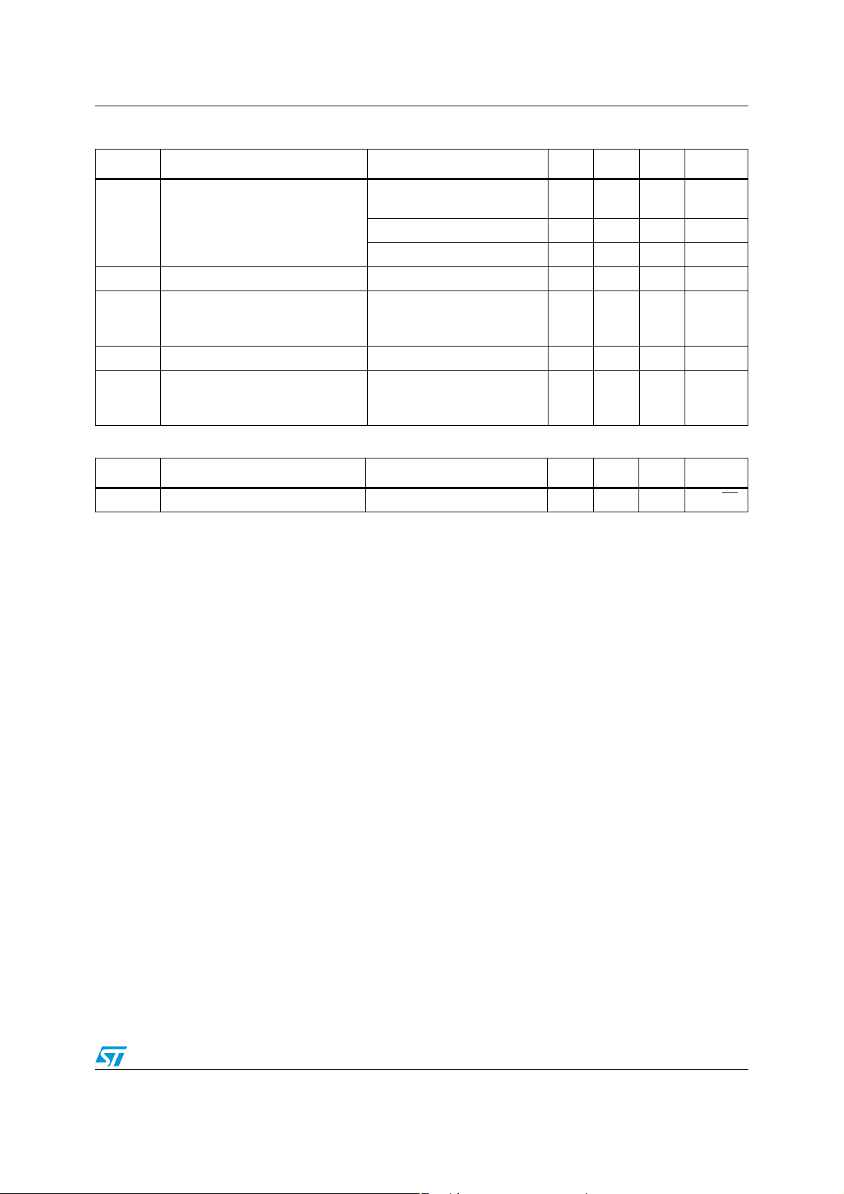
Table 7. Frequency response
Symbol Parameter Test conditions Min. Typ. Max. Unit
V
=10mV to 100mV,
sense
C
=47pF
ts Output settling to 1% of final value
load
Av = 50 V/V 6 µs
Av = 100 V/V 10 µs
t
SEL
t
SR Slew rate V
BW 3 dB bandwidth
Output settling to 1% of final value Any change of state of SEL 1 µs
Response to common-mode
voltage change.
rec
Output settling to 1% of final value
V
=5V, V
cc+
step change from -2 V to
V
m
=-5V
cc-
20 µs
30 V or 30 V to -2 V
=10mV to 100mV 0.4 0.6 V/µs
sense
C
V
load
sense
=47pF V
=50mV
icm
=12V
700 kHz
Av = 50 V/V
Table 8. Noise
Symbol Parameter Test conditions Min. Typ. Max. Unit
eN Equivalent input noise voltage f = 1 kHz 40 nV/√ Hz
Doc ID 16875 Rev 2 9/26
Page 10
Electrical characteristics curves: current sense amplifier TSC1031
-25
-20
-15
-10
-5
0
5
10
15
20
25
0 20 40 60 80 100
Icc (µA)
4 Electrical characteristics curves: current sense
amplifier
Unless otherwise specified, the test conditions for the following curves are:
● Tamb = 25°C, V
● No load on Out pin.
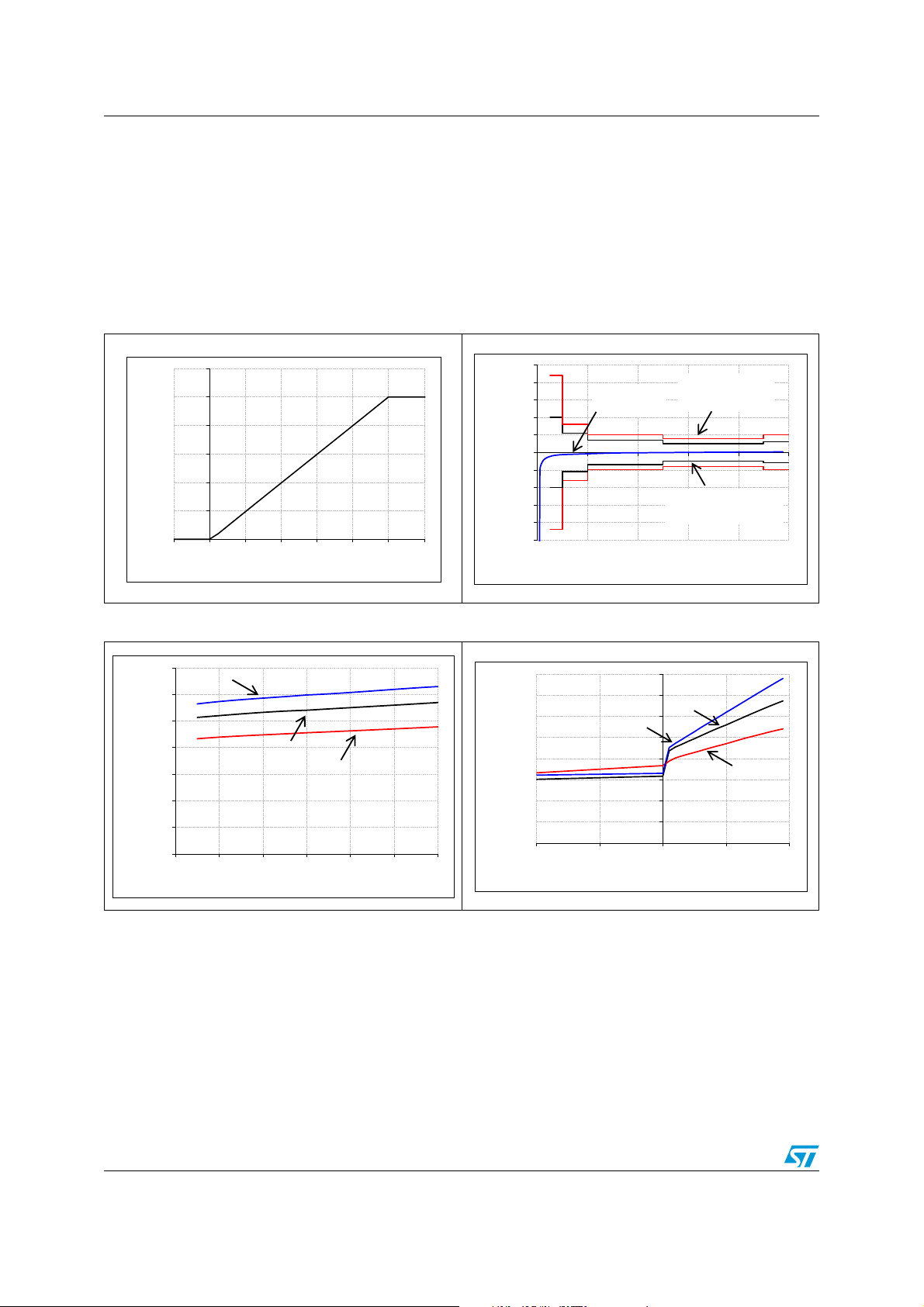
Figure 4. Output voltage vs. Vsense Figure 5. Output voltage accuracy vs. Vsense
6
5
4
3
2
Vout (V)
1
0
-20 0 20 40 60 80 100 120
Vsense (mV)
= 5 V, Vsense = Vp - Vm = 50 mV, Vm = 12 V.
CC
Typical
accuracy
delta in (%)
Vsense (mV)
Guaranteed
accuracy vs. T
Guaranteed
accuracy @ 25 °C
Figure 6. Supply current vs. supply voltage Figure 7. Supply current vs. Vsense
350
300
250
200
150
100
Icc (µA)
T = -40 °C
T = 25 °C
T = 125 °C
50
0
2.5 3 3.5 4 4.5 5 5.5
Vcc (V)
400
350
300
250
200
150
100
50
0
-100 -50 0 50 100
T = -40 °C
T = 25 °C
T = 125 °C
Vsense (mV)
10/26 Doc ID 16875 Rev 2
Page 11
TSC1031 Electrical characteristics curves: current sense amplifier
0
2
4
6
8
10
12
14
16
18
20
-100 -50 0 50 100
0
200
400
600
800
1000
1200
-10-8-6-4-2 0
T = 25 °C
T = 125 °C
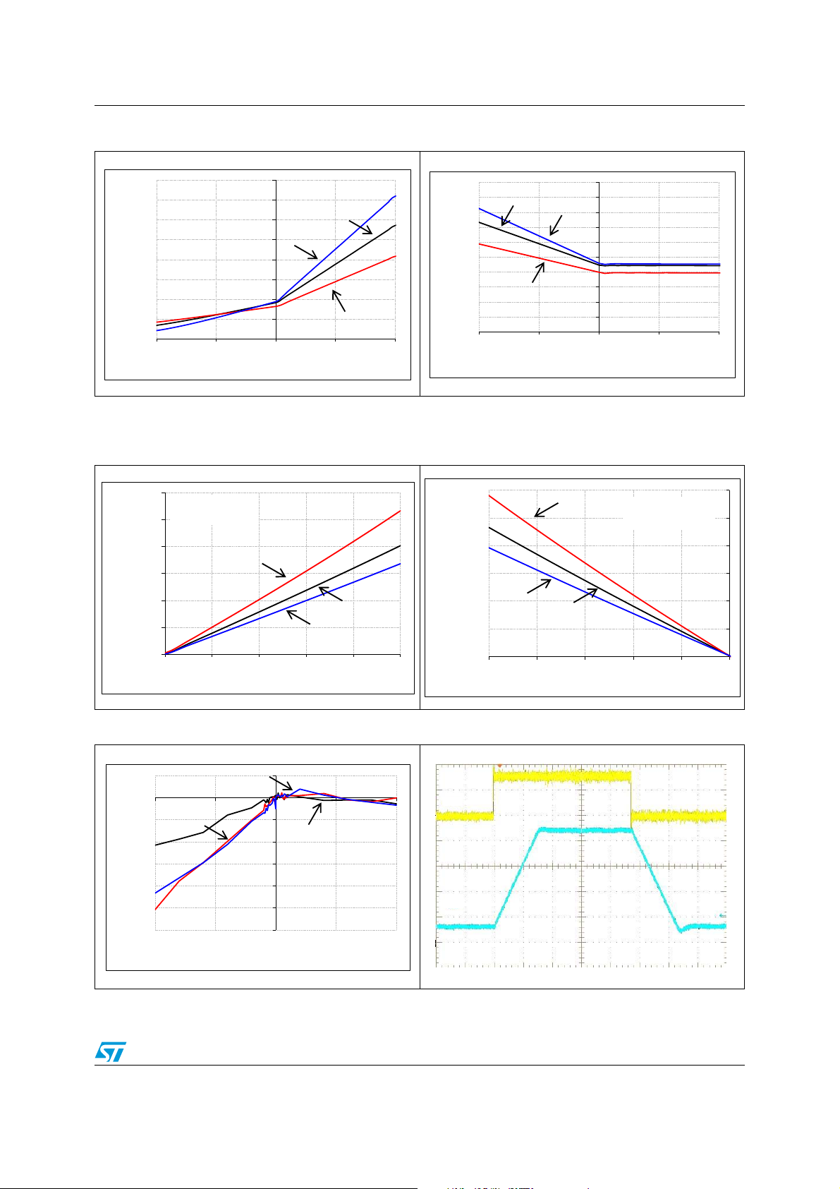
Figure 8. Vp pin input current vs. Vsense Figure 9. Vn pin input current vs. Vsense
40
35
30
25
T = 25 °C
T = -40 °C
20
15
Ip (µA)
10
5
0
T = 125 °C
-100 -50 0 50 100
Vsense (mV)
Figure 10. Output stage low-state saturation
voltage vs. output current
(Vsense = -1 V)
1200
1000
Output stage
sinking current
Im (µA)
Figure 11. Output stage high-state saturation
T = 25 °C
T = -40 °C
T = 125 °C
Vsense (mV)
voltage vs. output current
(Vsense = +1 V)
Output stage
sourcing current
800
600
400
Vol (mV)
200
0
0246810
Figure 12. Output stage load regulation Figure 13. Step response
1
0
-1
T = 125 °C
-2
-3
-4
-5
Output stage
sourcing current
-6
Vout - (Vout @ Iout = 0A) (mV)
-10 -5 0 5 10
T = 125 °C
Iout (mA)
T = -40 °C
Iout (mA)
T = -40 °C
T = 25 °C
T = 25 °C
Voh (mV)
T = -40 °C
Iout (mA)
Vsense
Output stage
sinking current
Vout
Time base 4µs/div
Vsense 50mV/div
Vout 500mV/div
Doc ID 16875 Rev 2 11/26
Page 12
Electrical characteristics curves: current sense amplifier TSC1031
0
5
10
15
20
25
30
35
40
45
50
1.E+01 1.E+02 1.E+03 1.E+04 1.E+05 1.E+06
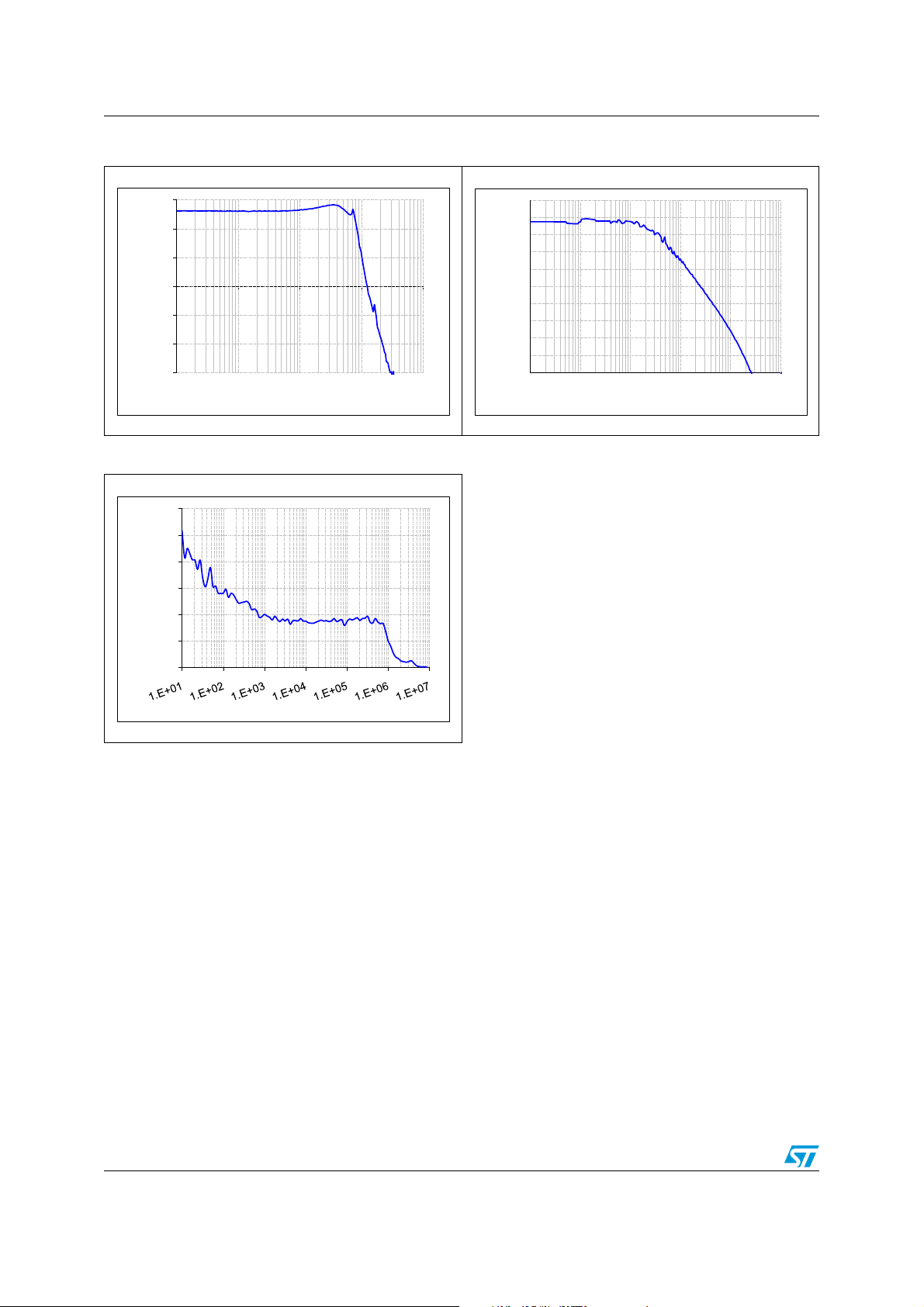
Figure 14. Bode diagram Figure 15. Power supply rejection ratio
30
20
10
0
-10
Gain (dB)
-20
-30
1.E+03 1.E+04 1.E+05 1.E+06 1.E+07
Frequency (Hz)
PSRR (dB)
Frequency (Hz)
Figure 16. Noise Level
120
100
80
60
40
20
0
Noise level (nv/sqrt(Hz))
Frequency (Hz)
12/26 Doc ID 16875 Rev 2
Page 13

TSC1031 Parameter definitions
5 Parameter definitions
5.1 Common mode rejection ratio (CMR)
The common mode rejection ratio (CMR) measures the ability of the current sensing
amplifier to reject any DC voltage applied on both inputs V
back to the input so that its effect can be compared with the applied differential signal. The
CMR is defined by the formula:
ΔV
CMR 20–
------------------------------log⋅=
ΔV
out
icm
5.2 Supply voltage rejection ratio (SVR)
The supply voltage rejection ratio (SVR) measures the ability of the current-sensing
amplifier to reject any variation of the supply voltage V
input so that its effect can be compared with the applied differential signal. The SVR is
defined by the formula:
Av⋅
and Vm. The CMR is referred
p
. The SVR is referred back to the
CC
ΔV
out
SVR 20–
------------------------------log⋅=
ΔV
CC
Av⋅
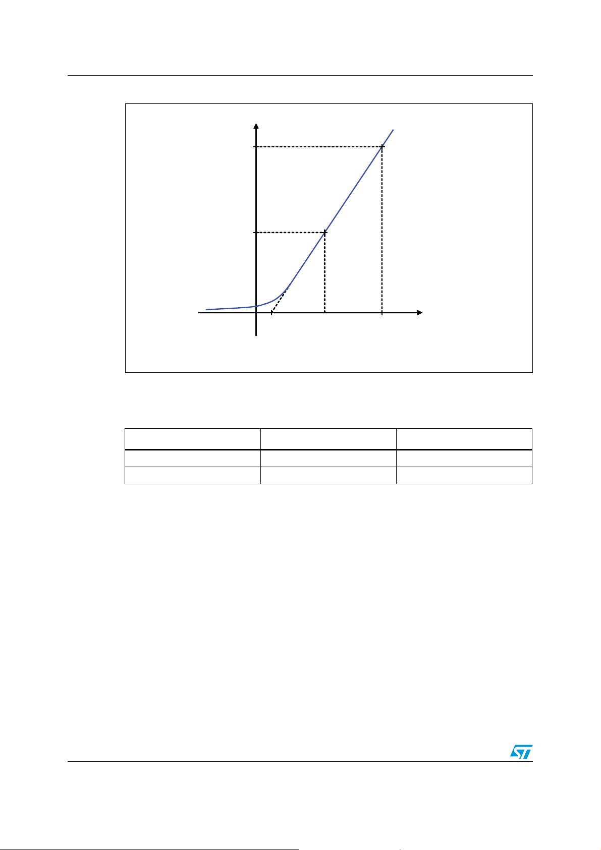
5.3 Gain (Av) and input offset voltage (Vos)
The input offset voltage is defined as the intersection between the linear regression of the
V
vs. V
out
V
sense=Vsense1
calculated with the following formula.
curve with the X-axis (see Figure 17.). If V
sense
and V
is the output voltage with V
out2
V
sense1Vsense2
⎛⎞
V
osVsense1
------------------------------------------------
–=
⎝⎠
V
–
–
out1Vout2
sense=Vsense2
V
⋅
is the output voltage with
out1
, then Vos can be
out1
Doc ID 16875 Rev 2 13/26
Page 14
Parameter definitions TSC1031
Figure 17. V
versus V
out
characteristics: detail for low V
sense
Vout
Vout_1
Vout_2
The values of V
sense1
and V
Vos Vsense2
used for the input offset calculations are detailed in
sense2
Vsense1
Ta bl e 9 .
Table 9. Test conditions for Vos voltage calculation
sense
Vsense
values
AM04520
Av (V/V) V
(mV) V
sense1
50 50 5
100 40 5
sense2
(mV)
14/26 Doc ID 16875 Rev 2
Page 15
TSC1031 Parameter definitions
-60
-40
-20
0
20
40
60
-60 -40 -20 0 20 40 60 80 100 120 140
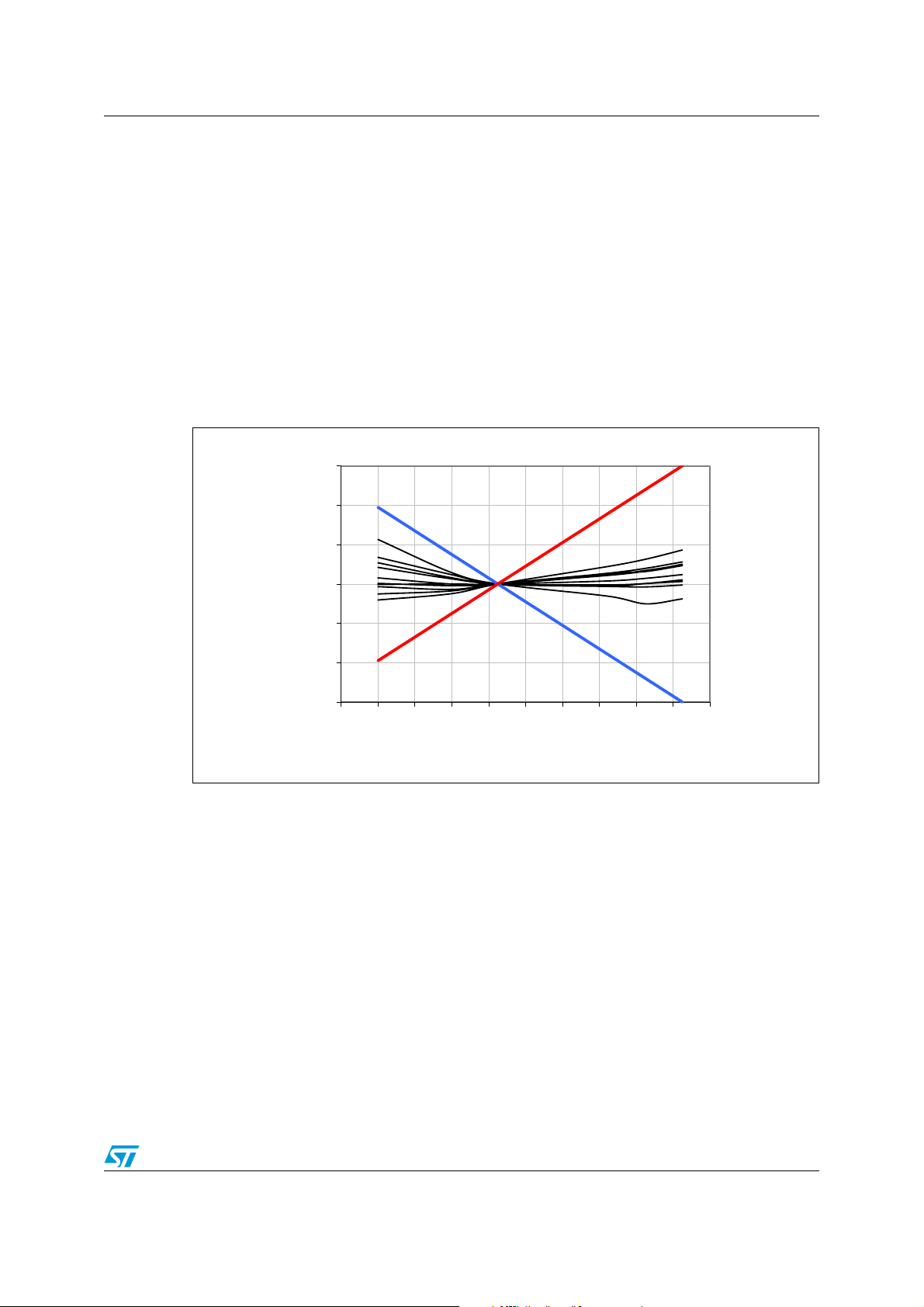
5.4 Output voltage drift versus temperature
The output voltage drift versus temperature is defined as the maximum variation of V
out
with
respect to its value at 25° C over the temperature range. It is calculated as follows:
with T
min
< T
amb
ΔV
-----------------max
ΔT
< T
max
.
out
V
()V
outTamb
--------------------------------------------------------------------------=
T
amb
25° C()–
out
25° C–
Figure 18 provides a graphical definition of the output voltage drift versus temperature. On
this chart V
V
versus T, and T = 25° C is considered to be the reference.
out
is always within the area defined by the maximum and minimum variation of
out
Figure 18. Output voltage drift versus temperature (Av = 50 V/V Vsense = 50 mV)
Vout-Vout@25°C (mV)
T (°C)
Doc ID 16875 Rev 2 15/26
Page 16
Parameter definitions TSC1031
T (°C)
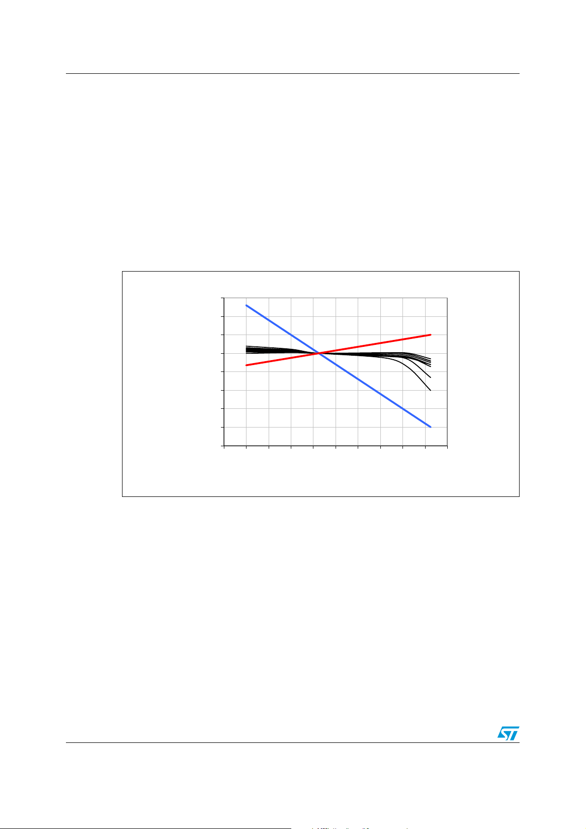
5.5 Input offset drift versus temperature
The input voltage drift versus temperature is defined as the maximum variation of Vos with
respect to its value at 25° C over the temperature range. It is calculated as follows:
with T
min
< T
amb
< T
ΔV
os
---------------max
ΔT
.
max
VosT
()Vos25° C()–
---------------------------------------------------------------------=
amb
T
amb
25° C–
Figure 19. provides a graphical definition of the input offset drift versus temperature. On this
chart V
V
os
is always comprised in the area defined by the maximum and minimum variation of
os
versus T, and T = 25° C is considered to be the reference.
Figure 19. Input offset drift versus temperature (Av = 50 V/V)
1.5
1
0.5
0
-0.5
-1
-1.5
Vos-Vos@25°C (mV)
-2
-2.5
-60 -40 -20 0 20 40 60 80 100 120 140
5.6 Output voltage accuracy
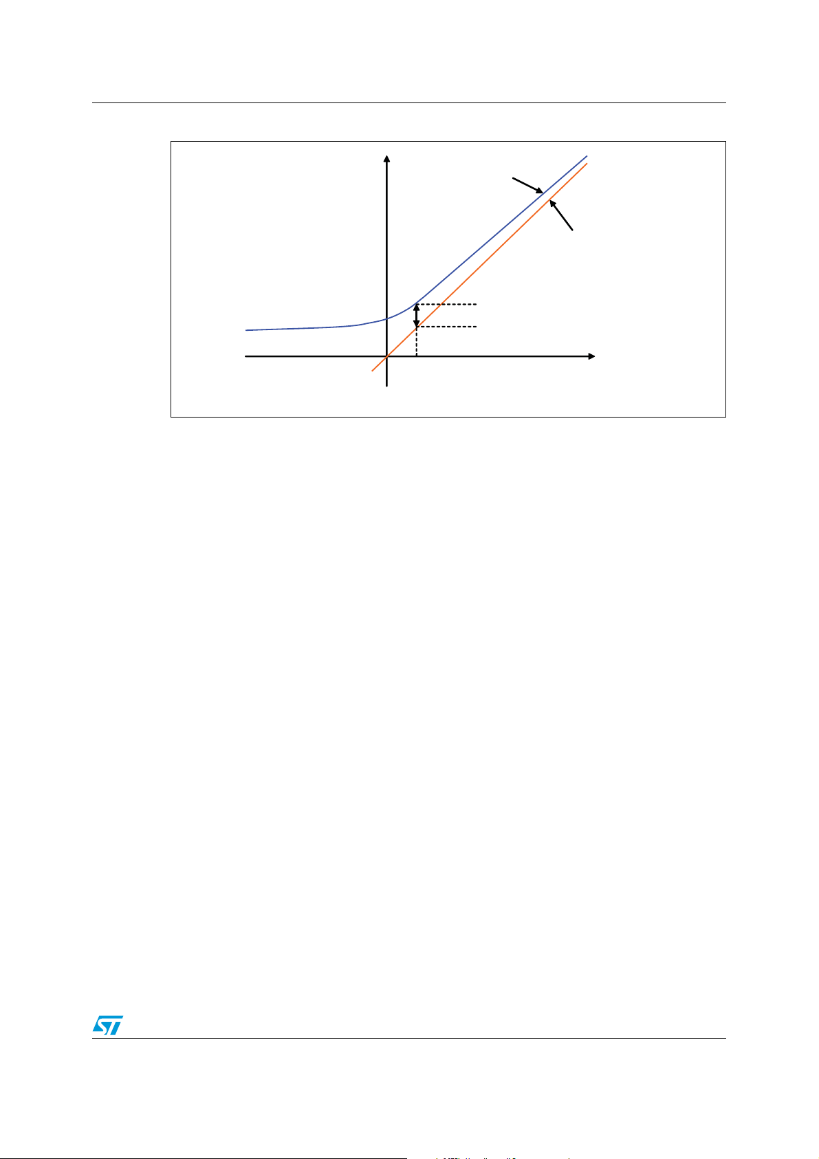
The output voltage accuracy is the difference between the actual output voltage and the
theoretical output voltage. Ideally, the current sensing output voltage should be equal to the
input differential voltage multiplied by the theoretical gain, as in the following formula.
V
= Av. V
out-th
The actual value is very slightly different, mainly due to the effects of:
● the input offset voltage V
● the non-linearity.
sense
os
,
16/26 Doc ID 16875 Rev 2
Page 17
TSC1031 Parameter definitions
Figure 20. Vout vs. Vsense theoretical and actual characteristics
Vout
5 mV
Actual
Ideal
Vout accuracy for Vsense = 5 mV
Vsense
AM04521
The output voltage accuracy, expressed as a percentage, can be calculated with the
following formula,
ΔV
out
abs V
---------------------------------------------------------------------------=
out
Av V
⋅
Av V
⋅()–()
sense
sense
with 50 V/V or 100 V/V depending on the configuration of the SEL pin.
Doc ID 16875 Rev 2 17/26
Page 18
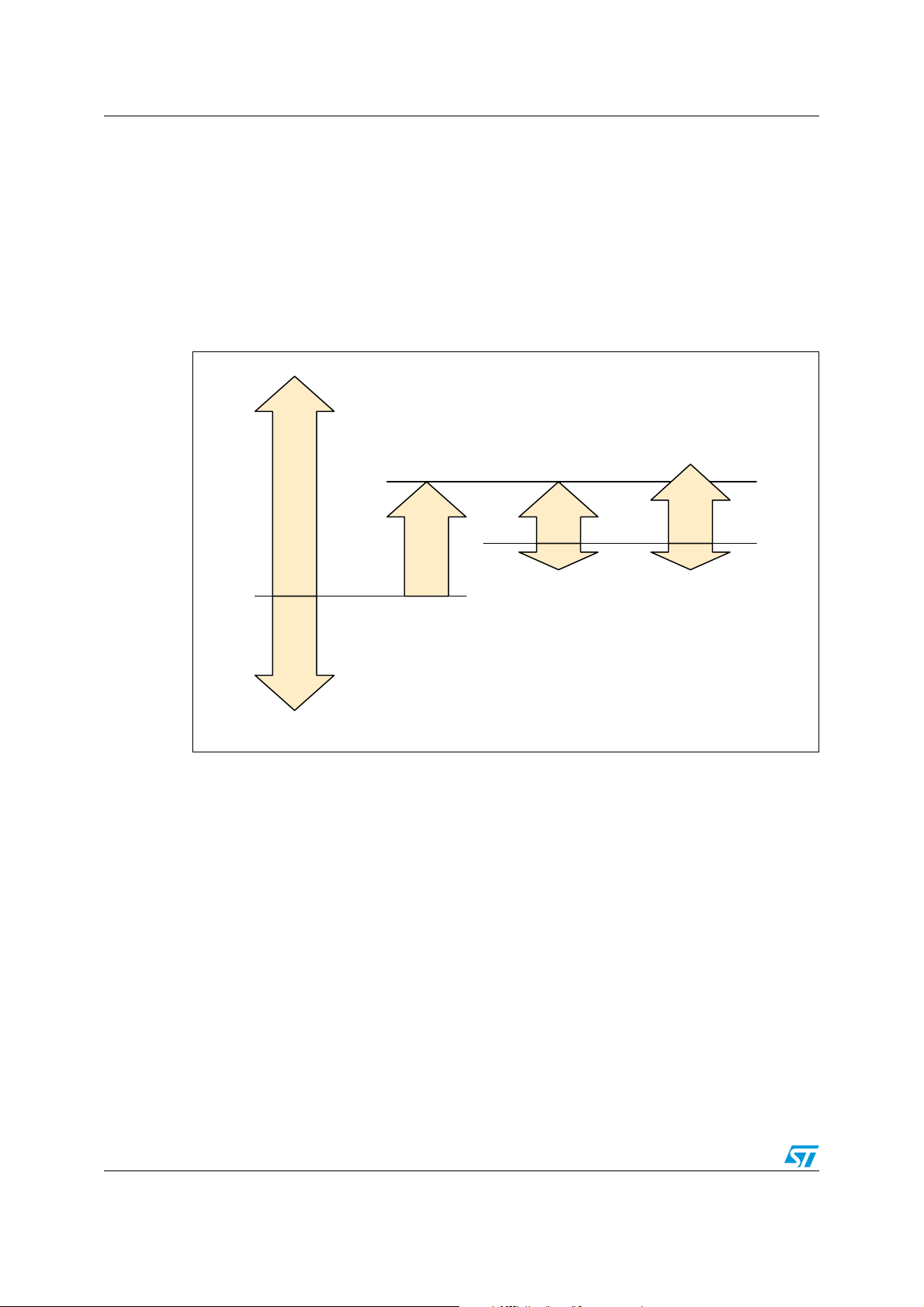
Maximum permissible voltages on pins TSC1031
6 Maximum permissible voltages on pins
The TSC1031 can be used in either single or dual supply configuration. The dual-supply
configuration is achieved by disconnecting Vcc- and Gnd, and connecting Vcc- to a negative
supply. Figure 21 illustrates how the absolute maximum voltages on input pins Vp and Vm
are referred to the Vcc- potential, while the maximum voltages on the positive supply pin,
gain selection pins and output pins are referred to the Gnd pin. It should also be noted that
the maximum voltage between Vcc- and Vcc+ is limited to 15 V.
Figure 21. Maximum voltages on pins
Vp and Vm
+75 V
SEL and Out
Vcc+
+15 V +7 V
Vcc+
Vcc+
+ 0.3 V
Vcc- Vcc-
-16 V
Vp and Vm
Gnd
-0.3V
Vcc+
Gnd
-0.3 V
SEL and Out
AM04528
18/26 Doc ID 16875 Rev 2
Page 19
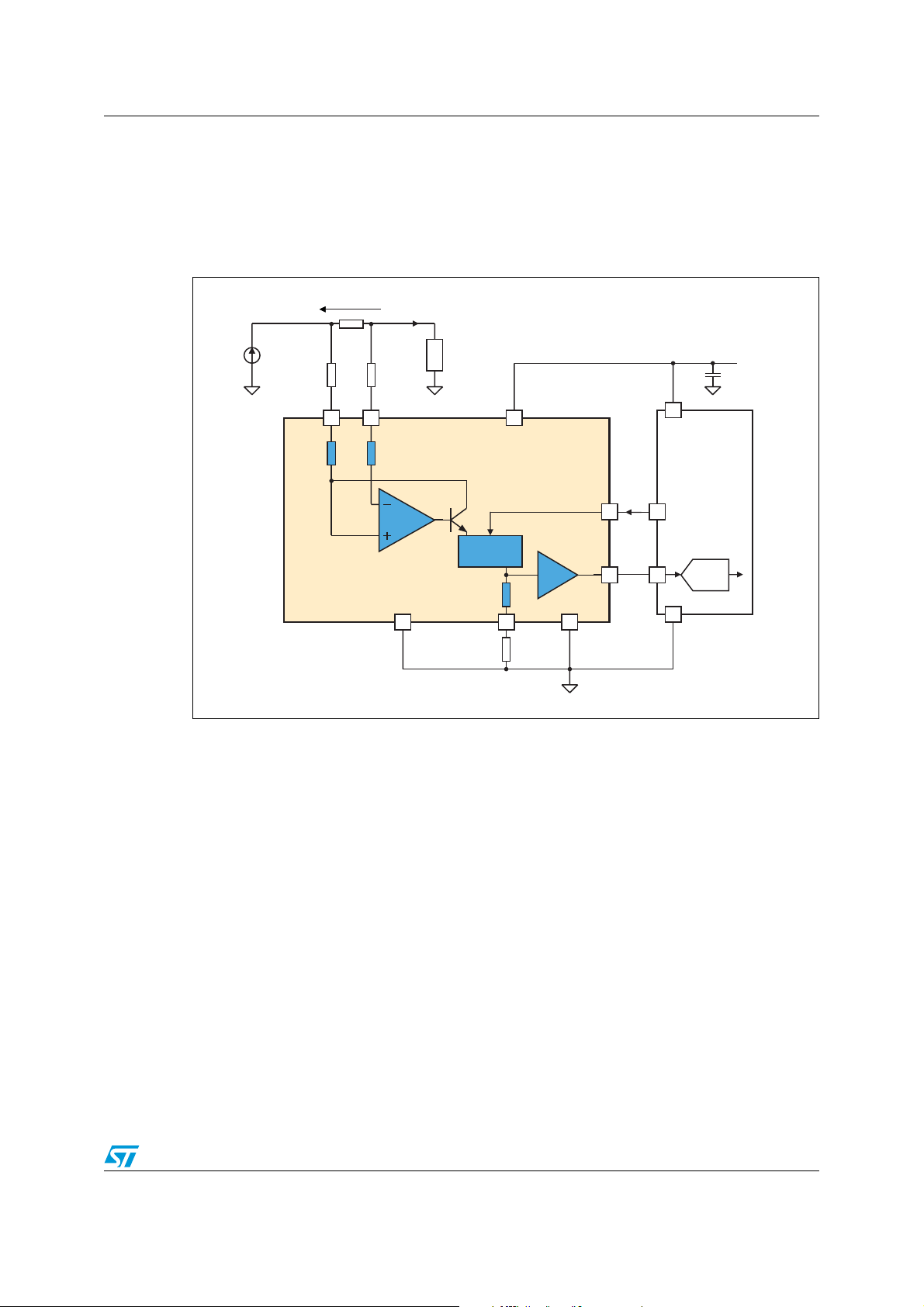
TSC1031 Application information
µ
7 Application information
The TSC1031 can be used to measure current and to feed back the information to a
microcontroller.
Figure 22. Typical application
Vsense
Iload
Rsense
Rf2Rf1
load
Common-mode voltage: 2.9 V to 70 V
5 V
Vp Vm
Rg1
5K
Sense
amplifier
TSC1031
Vcc-
Rg2
multiplier
Current
Vcc+
K2
2.5 or 5
Rg3
50K
SEL
x2
A1
Rf3
The current from the supply flows to the load through the R
drop equal to V
inverting input voltage is equal to V
sense
across R
. The amplifier’s input currents are negligible, therefore its
sense
. The amplifier's open-loop gain forces its non-inverting
m
Vout
Out
Gnd
resistor causing a voltage
sense
Vcc
GPIO
ADC
Gnd
Controller
AM06157
input to the same voltage as the inverting input. As a consequence, the amplifier adjusts
current flowing through Rg1 so that the voltage drop across Rg1 exactly matches V
Therefore, the drop across R
V
Rg1=Vsense=Rsense.Iload
If I
is the current flowing through Rg1, then I
Rg1
I
Rg1=Vsense/Rg1
The I
R
g3
current flows is multiplied by a ratio K2 and the resulting current flows into resistor
Rg1
. Therefore, the voltage drop on the Rg3 resistor can be calculated as follows.
V
Rg3=Rg3
.K2.I
Rg1
The voltage across the R
a gain equal to 2. Therefore V
V
= 2.K1.K2.V
or: V
out
out
= Av .R
sense
sense.Iload
is:
g1
is given by the formula:
Rg1
=(Rg3/Rg1).K2.V
resistor is buffered to the Out pin by the voltage buffer, featuring
g3
can be expressed as:
out
= Av .V
with Av= 2.K1.K2
sense
sense
=K1.K2.V
with K1=Rg3/Rg1=10.
sense
sense
.
Doc ID 16875 Rev 2 19/26
Page 20
Application information TSC1031
The current multiplier gain K2 can be set to 2.5 or 5 depending on the voltage applied on the
SEL pin.
Since they define the full-scale output range of the application, the R
resistor and the
sense
amplification gain Av are important parameters and must therefore be selected carefully.
The TSC1031’s dedicated schematic eases the implementation of EMI filtering in harsh
environments. A simple filter is described in Figure 22, where the input filtering is performed
by R
, Rf2 and Cf.
f1
The values of R
amplifier inputs. The value of the C
and Rf2 should be equal so as to balance the contribution on both
f1
capacitor should be selected so that the cut-off
f
frequency of the first-order low-pass filter provides enough attenuation to the high frequency
interferences.
To balance the contribution of R
resistor R
should be connected between pin A1 and Gnd. The value of Rf3 should be
f3
and Rf2 in the current sense amplifier gain, an output
f1
chosen according to the following formula.
K1 = 10 = R
g3/Rg1
= Rf3/R
= Rf3/R
f1
f2
If these precautions having been taken, the TSC1031’s gain is unaffected by the
implementation of the input filtering resistors.
20/26 Doc ID 16875 Rev 2
Page 21

TSC1031 Package information
8 Package information
In order to meet environmental requirements, ST offers these devices in different grades of
ECOPACK
specifications, grade definitions and product status are available at: www.st.com.
ECOPACK
®
packages, depending on their level of environmental compliance. ECOPACK®
®
is an ST trademark.
Doc ID 16875 Rev 2 21/26
Page 22
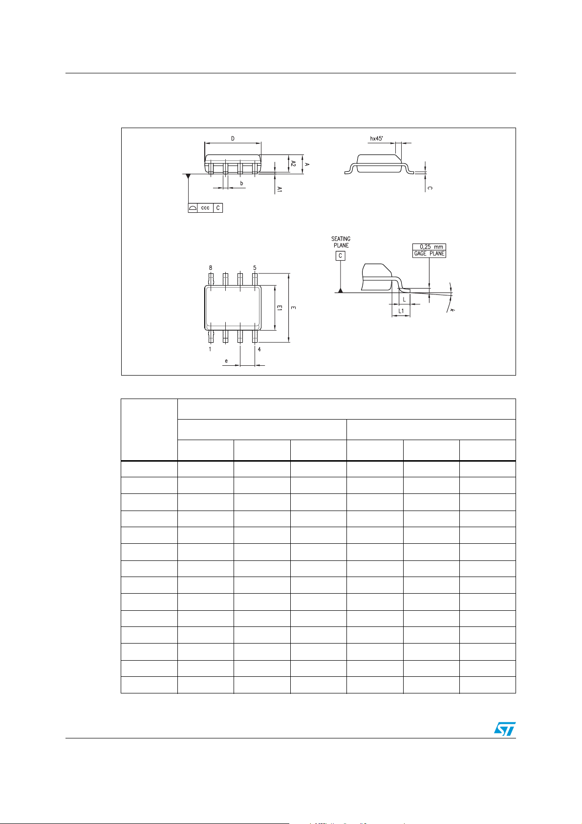
Package information TSC1031
8.1 SO-8 package information
Figure 23. SO-8 package mechanical drawing
Table 10. SO-8 package mechanical data
Dimensions
Ref.
Min. Typ. Max. Min. Typ. Max.
A1.750.069
A1 0.10 0.25 0.004 0.010
A2 1.25 0.049
b 0.28 0.48 0.011 0.019
c 0.17 0.23 0.007 0.010
D 4.80 4.90 5.00 0.189 0.193 0.197
E 5.80 6.00 6.20 0.228 0.236 0.244
E1 3.80 3.90 4.00 0.150 0.154 0.157
e 1.27 0.050
h 0.25 0.50 0.010 0.020
L 0.40 1.27 0.016 0.050
L1 1.04 0.040
k 0 8° 1° 8°
ccc 0.10 0.004
Millimeters Inches
22/26 Doc ID 16875 Rev 2
Page 23
TSC1031 Package information
8.2 TSSOP-8 package information
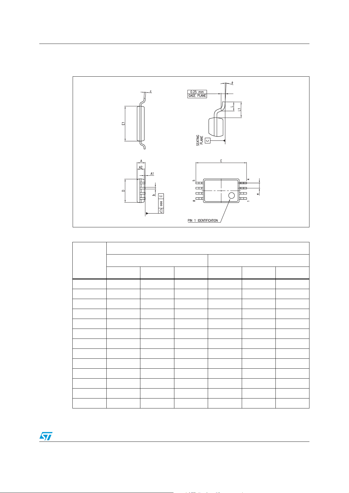
Figure 24. TSSOP8 package mechanical drawing
Table 11. TSSOP8 package mechanical data
Dimensions
Ref.
Min. Typ. Max. Min. Typ. Max.
A1.200.047
A1 0.05 0.15 0.002 0.006
A2 0.80 1.00 1.05 0.031 0.039 0.041
b 0.19 0.30 0.007 0.012
c 0.09 0.20 0.004 0.008
D 2.90 3.00 3.10 0.114 0.118 0.122
E 6.20 6.40 6.60 0.244 0.252 0.260
E1 4.30 4.40 4.50 0.169 0.173 0.177
e 0.65 0.0256
k0° 8°0° 8°
L 0.45 0.60 0.75 0.018 0.024 0.030
L1 1 0.039
aaa 0.10 0.004
Millimeters Inches
Doc ID 16875 Rev 2 23/26
Page 24
Ordering information TSC1031
9 Ordering information
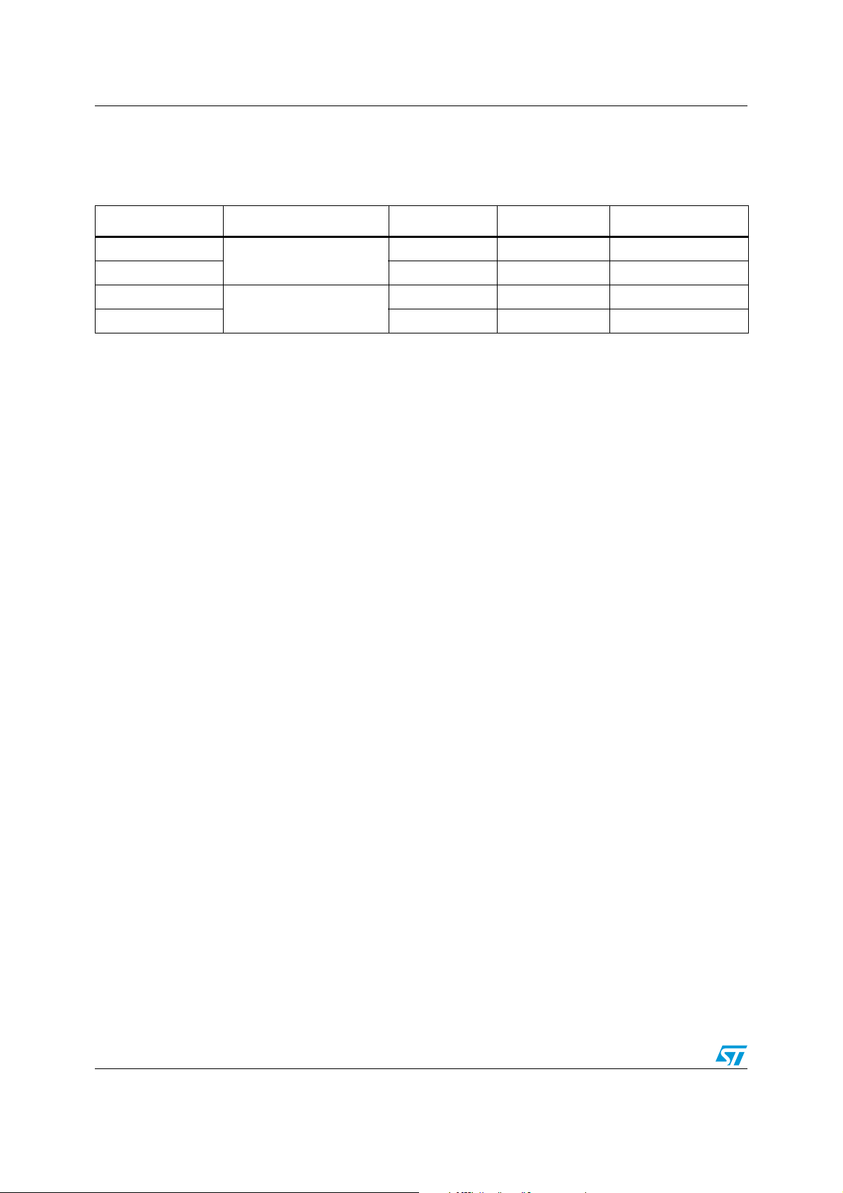
Table 12. Order codes
Part number Temperature range Package Packaging Marking
TSC1031IPT
-40°C, +125°C
TSC1031IDT SO-8 Tape & reel TSC1031I
TSC1031IYPT
TSC1031IYDT SO-8
1. Qualification and characterization according to AEC Q100 and Q003 or equivalent, advanced screening according to AEC
Q001 & Q002 or equivalent are on-going.
2. Qualification and characterization according to AEC Q100 and Q003 or equivalent, advanced screening according to AEC
Q001 & Q002 or equivalent.
-40°C, +125°C
Automotive grade
TSSOP8 Tape & reel 1031I
(2)
(1)
Tape & reel 1031Y
Tape & reel TSC1031Y
TSSOP8
24/26 Doc ID 16875 Rev 2
Page 25
TSC1031 Revision history
10 Revision history
Table 13. Document revision history
Date Revision Changes
04-Jan-2010 1 Initial release.
Added Chapter 4: Electrical characteristics curves: current
sense amplifier.
29-Apr-2011 2
Changed Figure 4 to Figure 16.
Modified Figure 22: Typical application.
Added automotive grade qualification for SO-8 package in
Table 12: Order codes.
Doc ID 16875 Rev 2 25/26
Page 26

TSC1031
Please Read Carefully:
Information in this document is provided solely in connection with ST products. STMicroelectronics NV and its subsidiaries (“ST”) reserve the
right to make changes, corrections, modifications or improvements, to this document, and the products and services described herein at any
time, without notice.
All ST products are sold pursuant to ST’s terms and conditions of sale.
Purchasers are solely responsible for the choice, selection and use of the ST products and services described herein, and ST assumes no
liability whatsoever relating to the choice, selection or use of the ST products and services described herein.
No license, express or implied, by estoppel or otherwise, to any intellectual property rights is granted under this document. If any part of this
document refers to any third party products or services it shall not be deemed a license grant by ST for the use of such third party products
or services, or any intellectual property contained therein or considered as a warranty covering the use in any manner whatsoever of such
third party products or services or any intellectual property contained therein.
UNLESS OTHERWISE SET FORTH IN ST’S TERMS AND CONDITIONS OF SALE ST DISCLAIMS ANY EXPRESS OR IMPLIED
WARRANTY WITH RESPECT TO THE USE AND/OR SALE OF ST PRODUCTS INCLUDING WITHOUT LIMITATION IMPLIED
WARRANTIES OF MERCHANTABILITY, FITNESS FOR A PARTICULAR PURPOSE (AND THEIR EQUIVALENTS UNDER THE LAWS
OF ANY JURISDICTION), OR INFRINGEMENT OF ANY PATENT, COPYRIGHT OR OTHER INTELLECTUAL PROPERTY RIGHT.
UNLESS EXPRESSLY APPROVED IN WRITING BY AN AUTHORIZED ST REPRESENTATIVE, ST PRODUCTS ARE NOT
RECOMMENDED, AUTHORIZED OR WARRANTED FOR USE IN MILITARY, AIR CRAFT, SPACE, LIFE SAVING, OR LIFE SUSTAINING
APPLICATIONS, NOR IN PRODUCTS OR SYSTEMS WHERE FAILURE OR MALFUNCTION MAY RESULT IN PERSONAL INJURY,
DEATH, OR SEVERE PROPERTY OR ENVIRONMENTAL DAMAGE. ST PRODUCTS WHICH ARE NOT SPECIFIED AS "AUTOMOTIVE
GRADE" MAY ONLY BE USED IN AUTOMOTIVE APPLICATIONS AT USER’S OWN RISK.
Resale of ST products with provisions different from the statements and/or technical features set forth in this document shall immediately void
any warranty granted by ST for the ST product or service described herein and shall not create or extend in any manner whatsoever, any
liability of ST.
ST and the ST logo are trademarks or registered trademarks of ST in various countries.
Information in this document supersedes and replaces all information previously supplied.
The ST logo is a registered trademark of STMicroelectronics. All other names are the property of their respective owners.
© 2011 STMicroelectronics - All rights reserved
STMicroelectronics group of companies
Australia - Belgium - Brazil - Canada - China - Czech Republic - Finland - France - Germany - Hong Kong - India - Israel - Italy - Japan -
Malaysia - Malta - Morocco - Philippines - Singapore - Spain - Sweden - Switzerland - United Kingdom - United States of America
www.st.com
26/26 Doc ID 16875 Rev 2
 Loading...