

Page 1
1.2 W differential input/output audio power amplifier
Features
■ Differential inputs
■ Near-zero pop & click
■ 100dB PSRR @ 217Hz with grounded inputs
■ Operating range from V
■ 1.2W rail-to-rail output power @ V
THD = 1%, F = 1kHz, with 8Ω
■ 90dB CMRR @ 217Hz
■ Ultra-low consumption in standby mode (10nA)
■ Selectable standby mode (active low or active
high)
■ Ultra fast startup time: 15ms typ.
■ Available in 9-bump flip-chip (300mm bump
diameter)
■ Lead-free package
= 2.5V to 5.5V
CC
CC
load
=5V,
TS4994FC
with selectable standb y
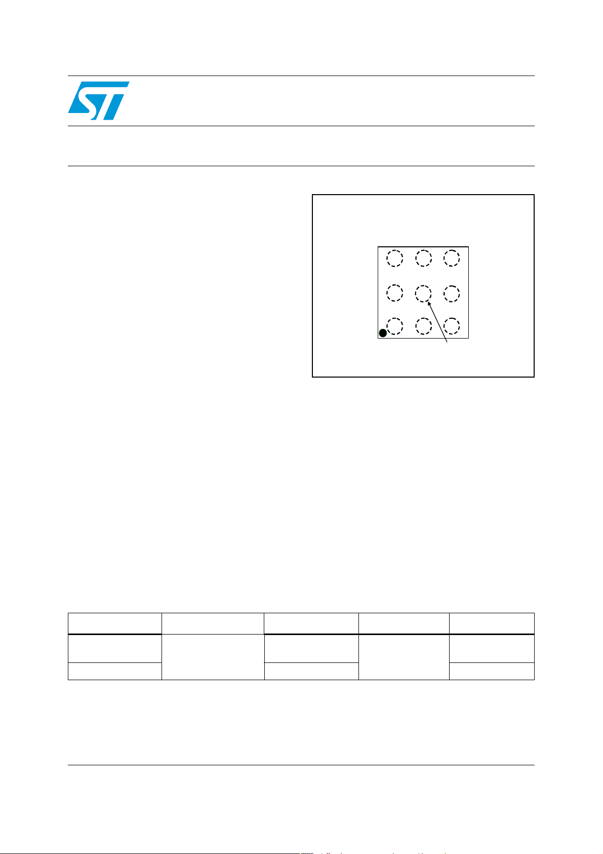
TS4994EIJT - Flip-chip (9 bumps)
Gnd
Gnd
V
V
Bypass Stdby
Bypass Stdby
V
V
765
765
O-
O-
8
8
1
1
IN+
IN+
9
9
2
2
V
V
CC
CC
The device is equipped with common mode
feedback circu itry allowing outputs to be always
biased at V
/2 regardless of the input common
CC
mode voltage.
V
V
O+
O+
4
4
V
V
3
3
IN-
IN-
Stdby Mode
Stdby Mode
Description
The TS4994 is an audio power amplifier capable
The TS4994 is designed for high quality audio
applications such as mobile phones and requir es
few external components.
of delivering 1W of continuous RMS output power
into an 8Ω load @ 5V. Due to its differential input s,
Applications
it exhibits outstanding noise immunity.
An external standby mode control reduces the
supply current to less than 10nA. An STBY
MODE pin allows the standby to be active HIGH
or LOW. An internal thermal shutdown protection
is also provided, making the device capable of
■ Mobile phones (cellular / cordless)
■ Laptop / notebook computers
■ PDAs
■ Portable audio devices
sustaining short-circuits.
Order codes
Part number Temperature range Package Packaging Marking
TS4994EIKJT
-40°C, +85°C
TS4994EIJT Lead free flip-chip9 A94
FC9 with back
coating
Tape & reel
A94
December 2006 Rev 2 1/35
www.st.com
35
Page 2

Contents TS4994FC
Contents
1 Application component information . . . . . . . . . . . . . . . . . . . . . . . . . . . . 3
2 Absolute maximum ratings and operating conditions . . . . . . . . . . . . . 4
3 Electrical characteristics . . . . . . . . . . . . . . . . . . . . . . . . . . . . . . . . . . . . . 5
4 Application information . . . . . . . . . . . . . . . . . . . . . . . . . . . . . . . . . . . . . 23
4.1 Differential configuration principle . . . . . . . . . . . . . . . . . . . . . . . . . . . . . . 23
4.2 Gain in typical application schematic . . . . . . . . . . . . . . . . . . . . . . . . . . . . 23
4.3 Common mode feedback loop limitations . . . . . . . . . . . . . . . . . . . . . . . . . 23
4.4 Low and high frequency response . . . . . . . . . . . . . . . . . . . . . . . . . . . . . . 24
4.5 Calculating the influence of mismatching on PSRR performance . . . . . . 25
4.6 CMRR performance . . . . . . . . . . . . . . . . . . . . . . . . . . . . . . . . . . . . . . . . . 27
4.7 Power dissipation and efficiency . . . . . . . . . . . . . . . . . . . . . . . . . . . . . . . 28
4.8 Decoupling of the circuit . . . . . . . . . . . . . . . . . . . . . . . . . . . . . . . . . . . . . . 30
4.9 Wake-up time: t
4.10 Shutdown time . . . . . . . . . . . . . . . . . . . . . . . . . . . . . . . . . . . . . . . . . . . . . 31
4.11 Pop performance . . . . . . . . . . . . . . . . . . . . . . . . . . . . . . . . . . . . . . . . . . . 31
4.12 Single-ended input configuration . . . . . . . . . . . . . . . . . . . . . . . . . . . . . . . 31
WU . . . . . . . . . . . . . . . . . . . . . . . . . . . . . . . . . . . . . . . . . . . . . . . . . . . . . . 30
5 Package information . . . . . . . . . . . . . . . . . . . . . . . . . . . . . . . . . . . . . . . . 32
6 Revision history . . . . . . . . . . . . . . . . . . . . . . . . . . . . . . . . . . . . . . . . . . . 34
2/35
Page 3
TS4994FC Application component information
1 Application component information
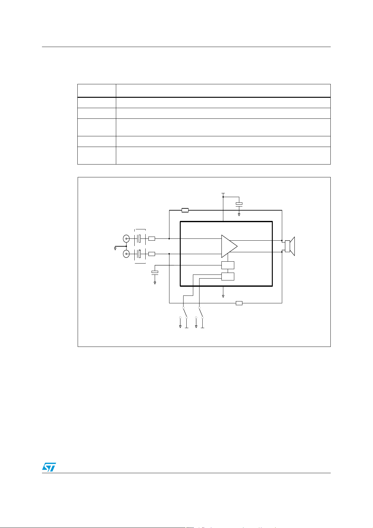
Components Functional description
C
s
C
b
R
feed
R
in
C
in
Supply bypass capacitor that provides power supply filtering.
Bypass capacitor that provides half supply filtering.
Feedback resistor that sets the closed loop gain in conjunction with Rin
AV= closed loop gain = R
Inverting input resistor that sets the closed loop gain in conjunction with R
Optional input capacitor making a high pass filter together with Rin.
(FCL= 1/(2πRinCin).
Figure 1. Typical application
Diff. input -
GND
Diff. Input +
Cin1
+
220nF
Cin2
+
220nF
Optional
Rin1
20k
Rin2
20k
GND
+
Cb
1u
.
feed/Rin
VCC
+
Cs
Rfeed1
20k
Vin-
3
Vin+
1
Bypass
8
Mode Stdby TS4994IJ
4
2
VCC
-
+
Standby
GND
69
GND
1u
GND
Bias
Rfeed2
20k
Vo+
Vo-
.
feed
5
7
8 Ohms
GND GNDVCC VCC
3/35
Page 4
Absolute maximum ratings and operating conditions TS4994FC
2 Absolute maximum ratings and operating conditions
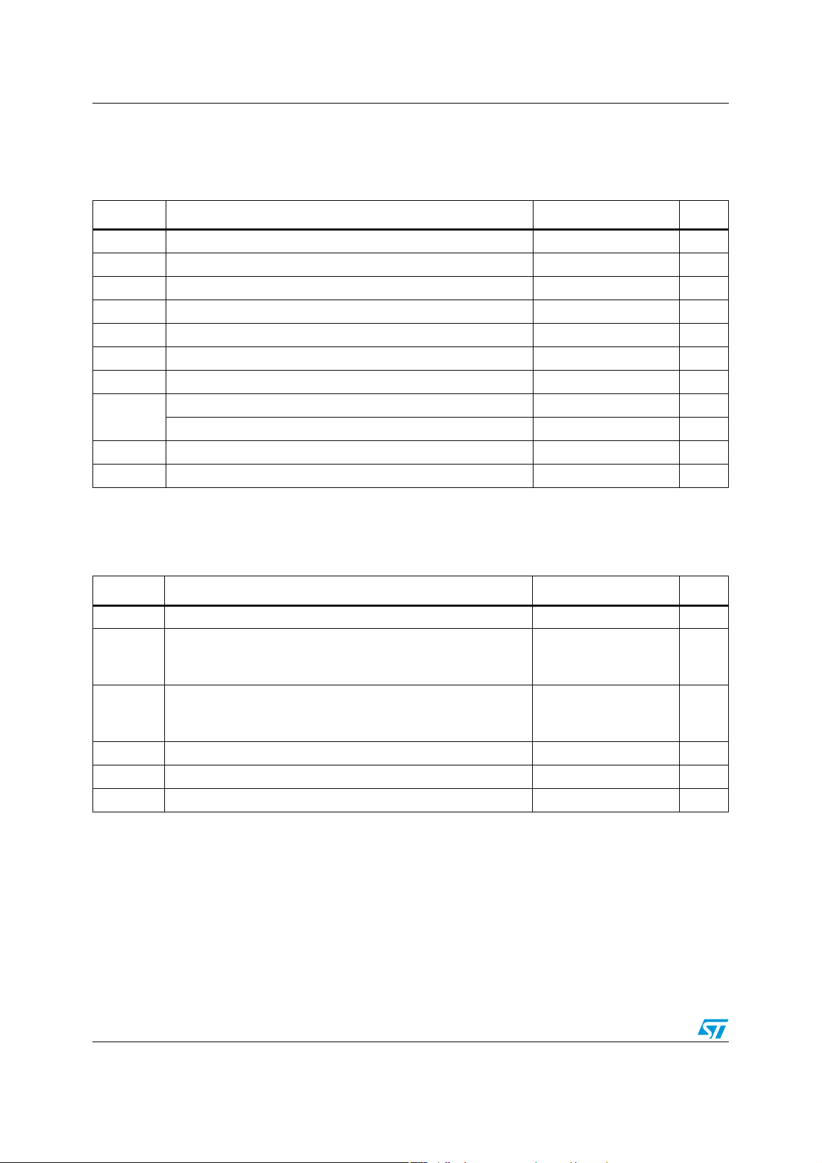
Table 1. Absolute maximum ratings
Symbol Parameter Value Unit
(2)
(1)
(3)
6V
GND to V
CC
250 °C/W
V
T
T
R
P
CC
V
oper
stg
T
thja
diss
Supply voltage
Input voltage
i
Operating free air tempe rature range -40 to + 85 °C
Storage temperature -65 to +150 °C
Maximum junction temperature 150 °C
j
Thermal resistance junction to ambient
Power dissipation internally limited W
Human body model 2 kV
ESD
Machine model 200 V
Latch-up immunity 200 mA
Lead temperature (soldering, 10sec) 260 °C
1. All voltage values are measured with respect to the ground pin.
2. The magnitude of the input signal must never exceed V
3. The device is protected by a thermal shutdown active at 150°C.
Table 2. Operating conditions
+ 0.3V / GND - 0.3V.
CC
V
Symbol Parameter Value Unit
V
CC
Supply voltage 2.5 to 5.5 V
Standby mode voltage input:
V
SM
Standby active LOW
Standby active HIGH
=GND
V
SM
VSM=V
CC
Standby voltage input:
V
STBY
T
SD
R
L
R
thja
1. The minimum current consumption (I
temperature range.
Device ON (VSM= GND) or device OFF (VSM=VCC)
Device OFF (V
= GND) or device ON (VSM=VCC)
SM
Thermal shutdown temperature 150 °C
Load resistor ≥ 4 Ω
Thermal resistance junction to ambient 100 °C/W
) is guaranteed when V
STBY
=GND or VCC (i.e. supply rails) for the whole
STBY
1.5 ≤ V
GND
≤ V
STBY
STBY
≤ VCC
≤ 0.4
(1)
V
V
4/35
Page 5
TS4994FC Electrical characteristics
3 Electrical characteristics
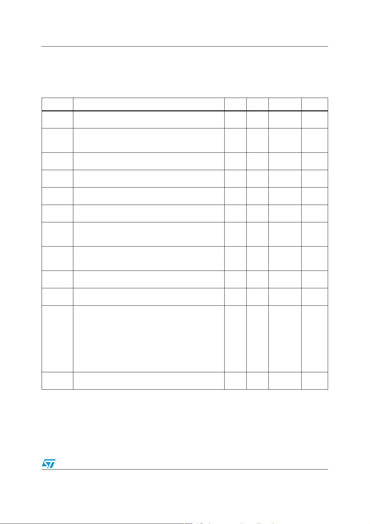
Table 3. Electrical characteristics for VCC = +5V, GND = 0V, T
= 25°C (unless otherwise
amb
specified)
Symbol Parameter Min. Typ. Max. Unit
I
CC
I
STBY
V
oo
V
ICM
P
out
THD + N
PSRR
CMRR
SNR
Supply current
No input signal, no load
Standby current
No input signal, V
No input signal, V
= VSM = GND, RL = 8Ω
STBY
= VSM = VCC, RL = 8Ω
STBY
Differential output offset voltage
No input signal, RL = 8Ω
Input common mode voltage
CMRR ≤ -60dB
Output power
THD = 1% Max, F= 1kHz, RL = 8Ω
Total harmonic distortion + noise
=850mW rms, AV=1, 20Hz ≤ F ≤ 20kHz, RL=8Ω
P
out
Power supply rejection ratio with inputs grounded
F = 217Hz, R = 8Ω, AV = 1, Cin = 4.7μF, Cb =1μF
IG
V
ripple
= 200mV
PP
Common mode rejection ratio
F = 217Hz, R
= 200mV
V
ic
= 8Ω, AV = 1, Cin = 4.7μF, Cb =1μF
L
PP
Signal-to-noise ratio (A-weighted filter, A
RL = 8Ω, THD +N < 0.7%, 20Hz ≤ F ≤ 20kHz
= 2.5)
V
(1)
47mA
10 1000 nA
0.1 10 mV
0.6 V
-0.9 V
CC
0.8 1.2 W
0.5 %
100 dB
90 dB
100 dB
GBP
Gain bandwidth product
R
= 8Ω
L
Output voltage noise, 20Hz ≤ F ≤ 20kHz, RL = 8Ω
Unweighted, A
A-weighted, A
Unweighted, A
V
N
A-weighted, A
Unweighted, A
A-weighted, A
= 1
V
= 1
V
= 2.5
V
= 2.5
V
= 7.5
V
= 7.5
V
Unweighted, Standby
A-weighted, Standby
t
WU
1. Dynamic measurements - 20*log(rms(V
2. Transition time from standby mode to fully operational amplifier.
Wake-up time
Cb =1μF
(2)
)/rms (V
out
ripple
)). V
ripple
5/35
2MHz
6
5.5
12
10.5
33
28
1.5
1
15 ms
is the super-imposed sinus signal relative to VCC.
μV
RMS
Page 6
Electrical characteristics TS4994FC
Table 4. Electrical characteristics for VCC = +3.3V (all electrical values are guaranteed with
correlation measurements at 2.6V and 5V), GND = 0V, T
= 25°C (unless otherwise
amb
specified)
Symbol Parameter Min. Typ. Max. Unit
I
CC
I
STBY
V
oo
V
ICM
P
out
THD + N
PSRR
CMRR
SNR
Supply current no input signal, no load 3 7 mA
Standby current
No input signal, V
No input signal, V
= VSM = GND, RL = 8Ω
STBY
= VSM = VCC, RL = 8Ω
STBY
Differential output offset voltage
No input signal, RL = 8Ω
Input common mode voltage
CMRR ≤ -60dB
Output power
THD = 1% max, F= 1kHz, R
= 8Ω
L
Total harmonic distortion + noise
= 300mW rms, AV = 1, 20Hz ≤ F ≤ 20kHz, RL = 8Ω
P
out
Power supply rejection ratio with inputs grounded
F = 217Hz, R = 8Ω, AV = 1, Cin = 4.7μF, Cb =1μF
IG
V
ripple
= 200mV
PP
0.6 V
300 500 mW
(1)
10 1000 nA
0.1 10 mV
-0.9 V
CC
0.5 %
100 dB
Common mode rejection ratio
F = 217Hz, R
= 200mV
V
ic
Signal-to-noise ratio (A-weighted filter, A
RL = 8Ω, THD +N < 0.7%, 20Hz ≤ F ≤ 20kHz
= 8Ω, AV = 1, Cin = 4.7μF, Cb =1μF
L
PP
= 2.5)
V
90 dB
100 dB
GBP
Gain bandwidth product
R
= 8Ω
L
Output voltage noise, 20Hz ≤ F ≤ 20kHz, RL = 8Ω
Unweighted, A
V
= 1
A-weighted, AV = 1
V
N
A-weighted, A
Unweighted, A
A-weighted, A
Unweighted, A
= 2.5
V
= 2.5
V
= 7.5
V
= 7.5
V
Unweighted, Standby
A-weighted, Standby
t
WU
1. Dynamic measurements - 20*log(rms(V
2. Transition time from standby mode to fully operational amplifier.
Wake-up time
Cb =1μF
(2)
)/rms (V
out
ripple
)). V
ripple
2MHz
6
5.5
12
10.5
33
28
1.5
1
15 ms
is the super-imposed sinus signal relative to VCC.
μV
RMS
6/35
Page 7
TS4994FC Electrical characteristics
Table 5. Electrical characteristics for VCC = +2.6V, GND = 0V, T
= 25°C (unless otherwise
amb
specified)
Symbol Parameter Min. Typ. Max. Unit
I
CC
I
STBY
V
V
ICM
P
out
THD + N
PSRR
CMRR
SNR
GBP
V
t
WU
Supply current
No input signal, no load
Standby current
No input signal, V
No input signal, V
Differential output offset voltage
oo
No input signal, R
= VSM = GND, RL = 8Ω
STBY
= VSM = VCC, RL = 8Ω
STBY
= 8Ω
L
Input common mode voltage
CMRR ≤ -60dB
Output power
THD = 1% max, F= 1kHz, RL = 8Ω
Total harmonic distortion + noise
= 225mW rms, AV = 1, 20Hz ≤ F ≤ 20kHz, RL = 8Ω
P
out
Power supply rejection ratio with inputs grounded
F = 217Hz, R = 8Ω, AV = 1, Cin = 4.7μF, Cb =1μF
IG
V
= 200mV
ripple
PP
Common mode rejection ratio
F = 217Hz, R
Vic = 200mV
= 8Ω, AV = 1, Cin = 4.7μF, Cb =1μF
L
PP
Signal-to-noise ratio (A-weighted filter, A
= 8Ω, THD +N < 0.7%, 20Hz ≤ F ≤ 20kHz
R
L
Gain bandwidth product
= 8Ω
R
L
Output voltage noise, 20Hz ≤ F ≤ 20kHz, RL = 8Ω
Unweighted, AV = 1
A-weighted, A
V
= 1
Unweighted, AV = 2.5
N
A-weighted, A
Unweighted, A
A-weighted, A
= 2.5
V
= 7.5
V
= 7.5
V
Unweighted, Standby
A-weighted, Standby
Wake-up time
(2)
Cb =1μF
= 2.5)
V
(1)
37mA
10 1000 nA
0.1 10 mV
0.6 V
- 0.9 V
CC
200 300 mW
0.5 %
100 dB
90 dB
100 dB
2MHz
6
5.5
12
10.5
33
28
1.5
1
15 ms
μV
RMS
1. Dynamic measurements - 20*log(rms(V
2. Transition time from standby mode to fully operational amplifier.
)/rms (V
out
ripple
)). V
ripple
7/35
is the super-imposed sinus signal relative to VCC.
Page 8
Electrical characteristics TS4994FC
0.0 0.6 1.2 1.8 2.4
0.0
0.5
1.0
1.5
2.0
2.5
3.0
Standby mode=0V
Standby mode=2.6V
Vcc = 2.6V
No load
Tamb=25°C
Current Consumption (mA)
Standby Voltage (V)
0.0 0.2 0.4 0.6 0.8 1.0 1.2 1.4 1.6
0.0
0.2
0.4
0.6
0.8
1.0
1.2
1.4
RL=16
Ω
RL=8
Ω
Vcc=5V
F=1kHz
THD+N<1%
RL=4
Ω
Power Dissipation (W)
Output Power (W)
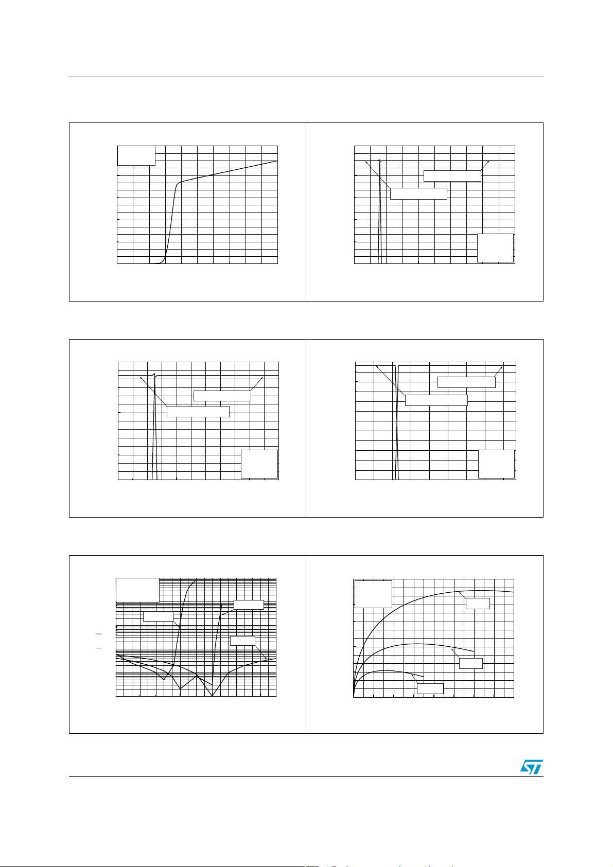
Figure 2. Current consumption vs. power
supply voltage
4.0
No load
Tamb=25°C
3.5
3.0
2.5
2.0
1.5
1.0
Current Consumption (mA)
0.5
0.0
012345
Power Supply Voltage (V)
Figure 4. Current consumption vs. standby
voltage
3.5
3.0
2.5
2.0
1.5
1.0
Current Consumption (mA)
0.5
0.0
0.0 0.6 1.2 1.8 2.4 3.0
Standby mode=0V
Standby mode=3.3V
Standby Voltage (V)
Vcc = 3.3V
No load
Tamb=25°C
Figure 3. Current consumption vs. standby
voltage
4.0
3.5
3.0
2.5
2.0
1.5
1.0
Current Consumption (mA)
0.5
0.0
012345
Standby mode=5V
Standby mode=0V
Standby Voltage (V)
Vcc = 5V
No load
Tamb=25°C
Figure 5. Current consumption vs. standby
voltage
Figure 6. Differential DC output voltage vs.
common mode input voltage
1000
Av = 1
Tamb = 25°C
100
10
Voo (mV)
1
0.1
0.01
0.0 0.5 1.0 1.5 2.0 2.5 3.0 3.5 4.0 4.5 5.0
8/35
Vcc=2.5V
Common Mode Input Voltage (V)
Figure 7. Power dissipation vs. output power
Vcc=3.3V
Vcc=5V
Page 9
TS4994FC Electrical characteristics
0.0 0.1 0.2 0.3 0.4
0.00
0.05
0.10
0.15
0.20
0.25
0.30
0.35
0.40
RL=4
Ω
RL=8
Ω
Vcc=2.6V
F=1kHz
THD+N<1%
RL=16
Ω
Power Dissipation (W)
Output Power (W)
2.5 3.0 3.5 4.0 4.5 5.0 5.5
0.0
0.2
0.4
0.6
0.8
1.0
1.2
1.4
1.6
1.8
2.0
THD+N=10%
RL = 8
Ω
F = 1kHz
BW < 125kHz
Tamb = 25°C
THD+N=1%
Output power (W)
Vcc (V)
2.5 3.0 3.5 4.0 4.5 5.0 5.5
0.0
0.1
0.2
0.3
0.4
0.5
0.6
THD+N=10%
RL = 32
Ω
F = 1kHz
BW < 125kHz
Tamb = 25°C
THD+N=1%
Output power (W)
Vcc (V)
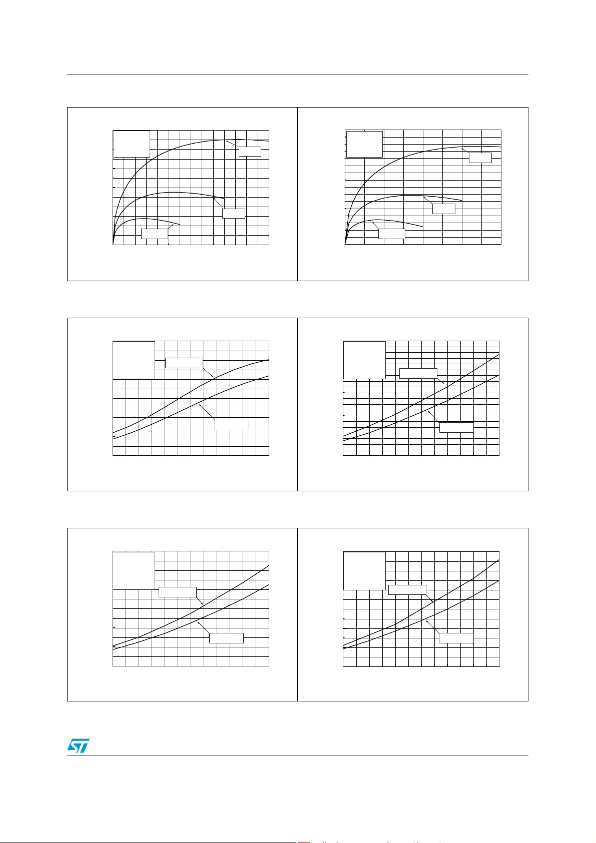
Figure 8. Power dissipation vs. outpu t power Figure 9. Power dissipation vs. output power
0.6
Vcc=3.3V
F=1kHz
0.5
THD+N<1%
0.4
0.3
0.2
Power Dissipation (W)
0.1
0.0
0.0 0.1 0.2 0.3 0.4 0.5 0.6 0.7
RL=16
Ω
Output Power (W)
Figure 10. Output power vs. power supply
voltage
2.4
RL = 4
2.2
2.0
1.8
1.6
1.4
1.2
1.0
0.8
Output power (W)
0.6
0.4
0.2
0.0
Ω
F = 1kHz
BW < 125kHz
Tamb = 25°C
2.5 3.0 3.5 4.0 4.5 5.0 5.5
THD+N=10%
Vcc (V)
RL=8
Ω
THD+N=1%
RL=4
Ω
Figure 11. Output power vs. power supply
voltage
Figure 12. Output power vs. power supply
voltage
1.2
RL = 16
Ω
F = 1kHz
1.0
BW < 125kHz
Tamb = 25°C
0.8
0.6
0.4
Output power (W)
0.2
0.0
2.5 3.0 3.5 4.0 4.5 5.0 5.5
THD+N=10%
Figure 13. Output power vs. power supply
voltage
THD+N=1%
Vcc (V)
9/35
Page 10
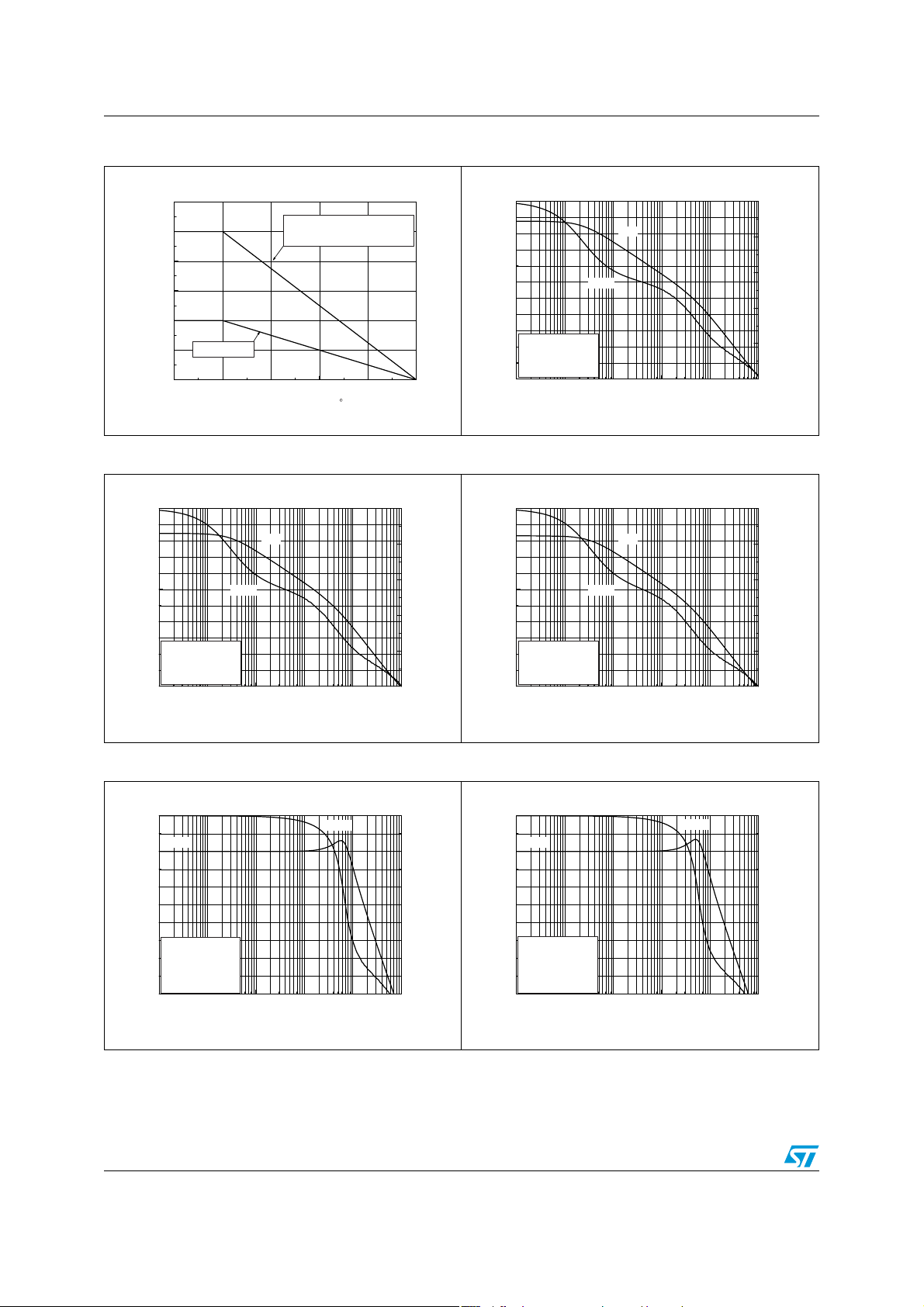
Electrical characteristics TS4994FC
Figure 14. Power derating curves Figure 15. Open loop gain vs. frequency
1.2
1.0
0.8
0.6
0.4
No Heat sink
0.2
Flip-Chip Package Power Dissipation (W)
0.0
0 25 50 75 100 125
Ambiant Temperature ( C)
Heat sink surface ≈ 100mm
(See demoboard)
2
60
40
20
Gain (dB)
0
Vcc = 5V
-20
ZL = 8Ω + 500pF
Tamb = 25°C
-40
0.1 1 10 100 1000 10000
Gain
Phase
Frequency (kHz)
Figure 16. Open loop gain vs. frequency Figure 17. Open loop gain vs. frequency
0
60
40
20
Gain (dB)
0
Phase
Gain
-40
-80
-120
Phase (°)
60
40
20
Gain (dB)
0
Gain
Phase
0
-40
-80
-120
-160
-200
0
-40
-80
-120
Phase (°)
Phase (°)
Vcc = 3.3V
-20
ZL = 8Ω + 500pF
Tamb = 25°C
-40
0.1 1 10 100 1000 10000
Frequency (kHz)
-160
-200
Vcc = 2.6V
-20
ZL = 8Ω + 500pF
Tamb = 25°C
-40
0.1 1 10 100 1000 10000
Frequency (kHz)
-160
-200
Figure 18. Closed loop gain vs. frequency Figure 19. Closed loop gain vs. frequency
10
Gain
0
-10
-20
Gain (dB)
Vcc = 5V
-30
Av = 1
ZL = 8Ω + 500pF
Tamb = 25°C
-40
0.1 1 10 100 1000 10000
Frequency (kHz)
Phase
0
-40
-80
-120
-160
-200
10
Gain
0
-10
Phase (°)
-20
Gain (dB)
Vcc = 3.3V
-30
Av = 1
ZL = 8Ω + 500pF
Tamb = 25°C
-40
0.1 1 10 100 1000 10000
Frequency (kHz)
Phase
0
-40
-80
-120
-160
-200
Phase (°)
10/35
Page 11
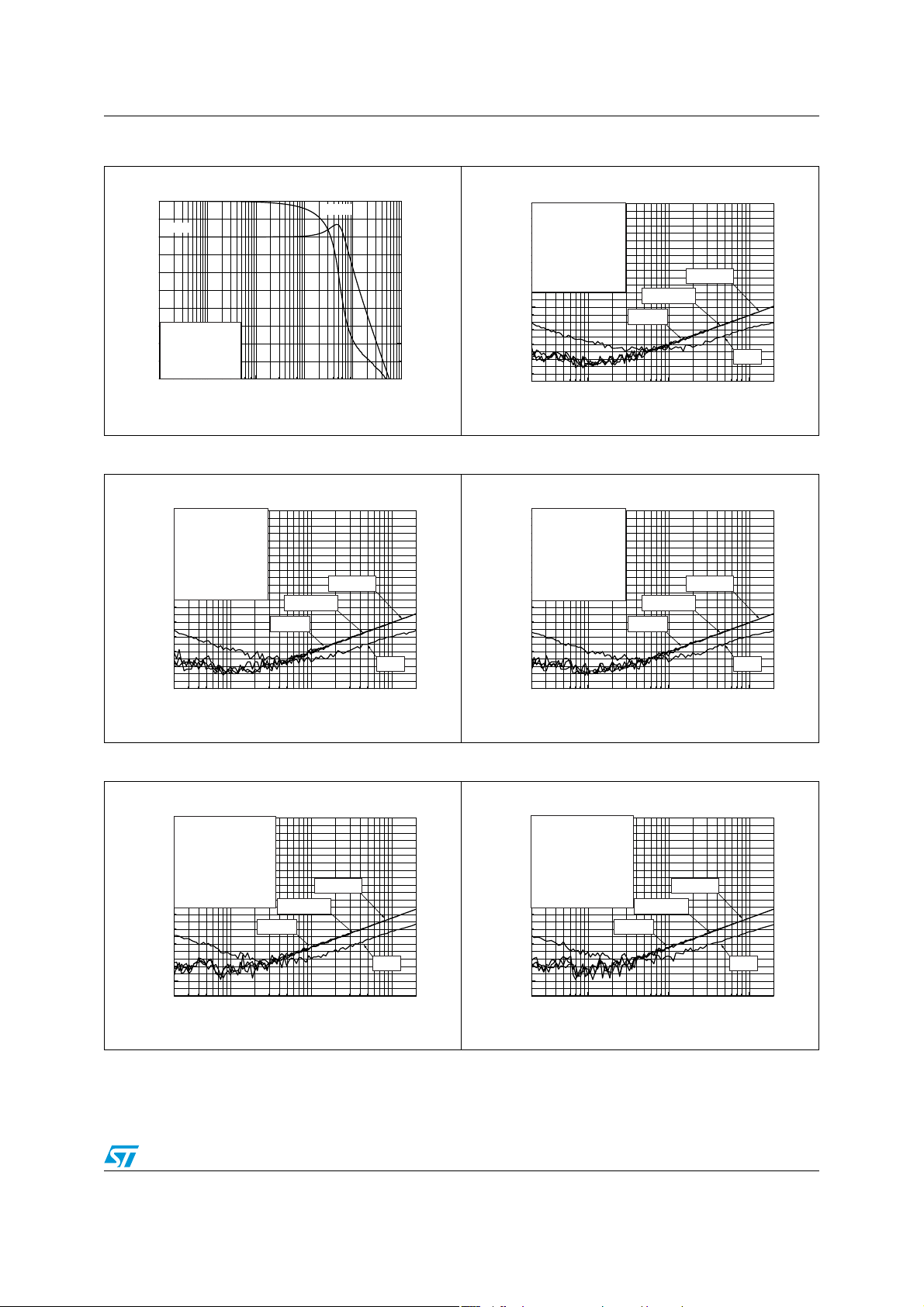
TS4994FC Electrical characteristics
100 1000 10000
-120
-110
-100
-90
-80
-70
-60
-50
-40
-30
-20
-10
0
Cb=0.1μF
Cb=1μF
Cb=0
20k
20
Cb=0.47μF
Vcc = 5V
Vripple = 200mVpp
Inputs = Grounded
Av = 1, Cin = 4.7μF
RL ≥ 8
Ω
Tamb = 25°C
PSRR (dB)
Frequency (Hz)
100 1000 10000
-120
-110
-100
-90
-80
-70
-60
-50
-40
-30
-20
-10
0
Cb=0.1μF
Cb=1μF
Cb=0
20k
20
Cb=0.47μF
Vcc = 2.6V
Vripple = 200mVpp
Inputs = Grounded
Av = 1, Cin = 4.7μF
RL ≥ 8
Ω
Tamb = 25°C
PSRR (dB)
Frequency (Hz)
100 1000 10000
-120
-110
-100
-90
-80
-70
-60
-50
-40
-30
-20
-10
0
Cb=0.1μF
Cb=1μF
Cb=0
20k
20
Cb=0.47μF
Vcc = 3.3V
Vripple = 200mVpp
Inputs = Grounded
Av = 2.5, Cin = 4.7μF
RL ≥ 8
Ω
Tamb = 25°C
PSRR (dB)
Frequency (Hz)
Figure 20. Closed loop gain vs. frequency Figure 21. PSRR vs. frequency
10
Gain
0
-10
-20
Gain (dB)
Vcc = 2.6V
-30
Av = 1
ZL = 8Ω + 500pF
Tamb = 25°C
-40
0.1 1 10 100 1000 10000
Frequency (kHz)
Phase
0
-40
-80
-120
-160
-200
Phase (°)
Figure 22. PSRR vs. frequency Figure 23. PSRR vs. frequency
0
-10
Vcc = 3.3V
Vripple = 200mVpp
-20
Inputs = Grounded
-30
Av = 1, Cin = 4.7μF
-40
RL ≥ 8
-50
-60
-70
PSRR (dB)
-80
-90
-100
-110
-120
Tamb = 25°C
20
Ω
Cb=1μF
100 1000 10000
Frequency (Hz)
Cb=0.1μF
Cb=0.47μF
Cb=0
20k
Figure 24. PSRR vs. frequency Figure 25. PSRR vs. frequency
0
-10
Vcc = 5V
Vripple = 200mVpp
-20
Inputs = Grounded
-30
Av = 2.5, Cin = 4.7μF
-40
RL ≥ 8
Tamb = 25°C
20
Ω
100 1000 10000
-50
-60
-70
PSRR (dB)
-80
-90
-100
-110
-120
Cb=1μF
Frequency (Hz)
Cb=0.47μF
Cb=0.1μF
Cb=0
20k
11/35
Page 12
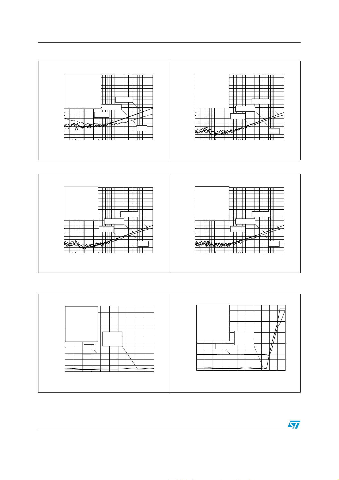
Electrical characteristics TS4994FC
100 1000 10000
-120
-110
-100
-90
-80
-70
-60
-50
-40
-30
-20
-10
0
Cb=0.1μF
Cb=1μF
Cb=0
20k
20
Cb=0.47μF
Vcc = 5V
Vripple = 200mVpp
Inputs = Floating
Rfeed = 20k
Ω
RL ≥ 8
Ω
Tamb = 25°C
PSRR (dB)
Frequency (Hz)
100 1000 10000
-120
-110
-100
-90
-80
-70
-60
-50
-40
-30
-20
-10
0
Cb=0.1μF
Cb=1μF
Cb=0
20k
20
Cb=0.47μF
Vcc = 2.6V
Vripple = 200mVpp
Inputs = Floating
Rfeed = 20k
Ω
RL ≥ 8
Ω
Tamb = 25°C
PSRR (dB)
Frequency (Hz)
0.0 0.6 1.2 1.8 2.4 3.0
-100
-80
-60
-40
-20
0
Cb=1μF
Cb=0.47μF
Cb=0.1μF
Cb=0
Vcc = 3.3V
Vripple = 200mVpp
Inputs Grounded
F = 217Hz
Av = 1
RL ≥ 8
Ω
Tamb = 25°C
PSRR(dB)
Common Mode Input Voltage (V)
Figure 26. PSRR vs. frequency Figure 27. PSRR vs. frequency
0
-10
Vcc = 2.6V
-20
Vripple = 200mVpp
Inputs = Grounded
-30
Av = 2.5, Cin = 4.7μF
-40
RL ≥ 8
-50
-60
-70
PSRR (dB)
-80
-90
-100
-110
-120
Tamb = 25°C
20
Ω
Cb=1μF
100 1000 10000
Frequency (Hz)
Cb=0.1μF
Cb=0.47μF
Cb=0
20k
Figure 28. PSRR vs. frequency Figure 29. PSRR vs. frequency
0
-10
Vcc = 3.3V
Vripple = 200mVpp
-20
Inputs = Floating
-30
-40
-50
-60
-70
PSRR (dB)
-80
-90
-100
-110
-120
Rfeed = 20k
RL ≥ 8
Tamb = 25°C
20
Ω
Ω
Cb=1μF
100 1000 10000
Frequency (Hz)
Cb=0.1μF
Cb=0.47μF
Cb=0
20k
Figure 30. PSRR vs. common mode input
voltage
0
Vcc = 5V
Vripple = 200mVpp
-20
Inputs Grounded
F = 217Hz
Av = 1
-40
RL ≥ 8
Ω
Tamb = 25°C
-60
PSRR(dB)
-80
-100
012345
Common Mode Input Voltage (V)
12/35
Cb=0
Cb=1μF
Cb=0.47μF
Cb=0.1μF
Figure 31. PSRR vs. common mode input
voltage
Page 13
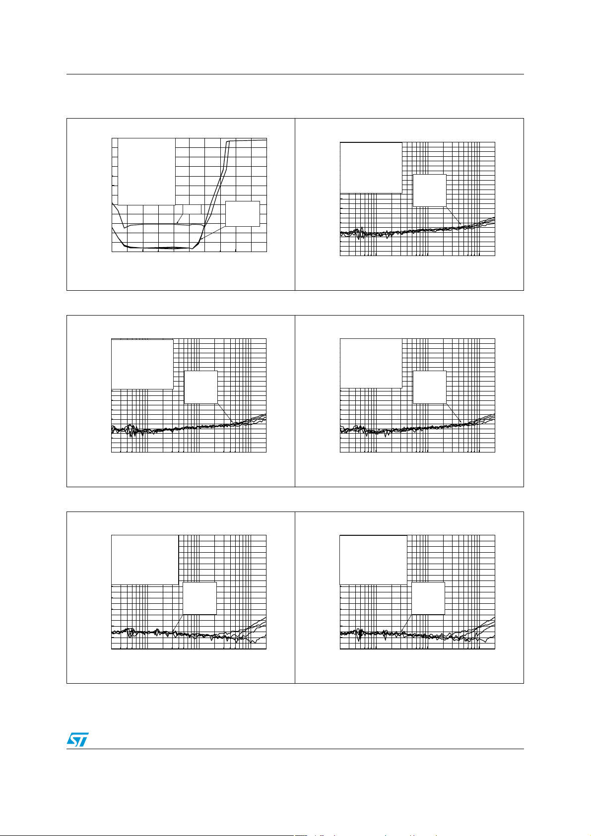
TS4994FC Electrical characteristics
100 1000 10000
-120
-110
-100
-90
-80
-70
-60
-50
-40
-30
-20
-10
0
Cb=1μF
Cb=0.47μF
Cb=0.1μF
Cb=0
20k
20
Vcc = 5V
Vic = 200mVpp
Av = 1, Cin = 470μF
RL ≥ 8
Ω
Tamb = 25°C
CMRR (dB)
Frequency (Hz)
100 1000 10000
-120
-110
-100
-90
-80
-70
-60
-50
-40
-30
-20
-10
0
Cb=1μF
Cb=0.47μF
Cb=0.1μF
Cb=0
20k
20
Vcc = 2.6V
Vic = 200mVpp
Av = 1, Cin = 470μF
RL ≥ 8
Ω
Tamb = 25°C
CMRR (dB)
Frequency (Hz)
100 1000 10000
-100
-90
-80
-70
-60
-50
-40
-30
-20
-10
0
Cb=1μF
Cb=0.47μF
Cb=0.1μF
Cb=0
20k
20
Vcc = 3.3V
Vic = 200mVpp
Av = 2.5, Cin = 470μF
RL ≥ 8
Ω
Tamb = 25°C
CMRR (dB)
Frequency (Hz)
Figure 32. PSRR vs. common mode input
Figure 33. CMRR vs. frequency
voltage
0
Vcc = 2.5V
Vripple = 200mVpp
Inputs Grounded
-20
F = 217Hz
Av = 1
-40
RL ≥ 8Ω
Tamb = 25°C
-60
PSRR(dB)
-80
-100
0.0 0.5 1.0 1.5 2.0 2.5
Common Mode Input Voltage (V)
Cb=0
Cb=1μF
Cb=0.47μF
Cb=0.1μF
Figure 34. CMRR vs. frequency Figure 35. CMRR vs. frequency
0
-10
Vcc = 3.3V
Vic = 200mVpp
-20
Av = 1, Cin = 470μF
-30
RL ≥ 8
CMRR (dB)
-100
-110
-120
-40
-50
-60
-70
-80
-90
20
Ω
Tamb = 25°C
100 1000 10000
Cb=1μF
Cb=0.47μF
Cb=0.1μF
Cb=0
Frequency (Hz)
20k
Figure 36. CMRR vs. frequency Figure 37. CMRR vs. frequency
0
Vcc = 5V
-10
Vic = 200mVpp
-20
Av = 2.5, Cin = 470μF
RL ≥ 8
Tamb = 25°C
20
Ω
Cb=1μF
Cb=0.47μF
Cb=0.1μF
Cb=0
100 1000 10000
Frequency (Hz)
20k
13/35
-30
-40
-50
-60
CMRR (dB)
-70
-80
-90
-100
Page 14
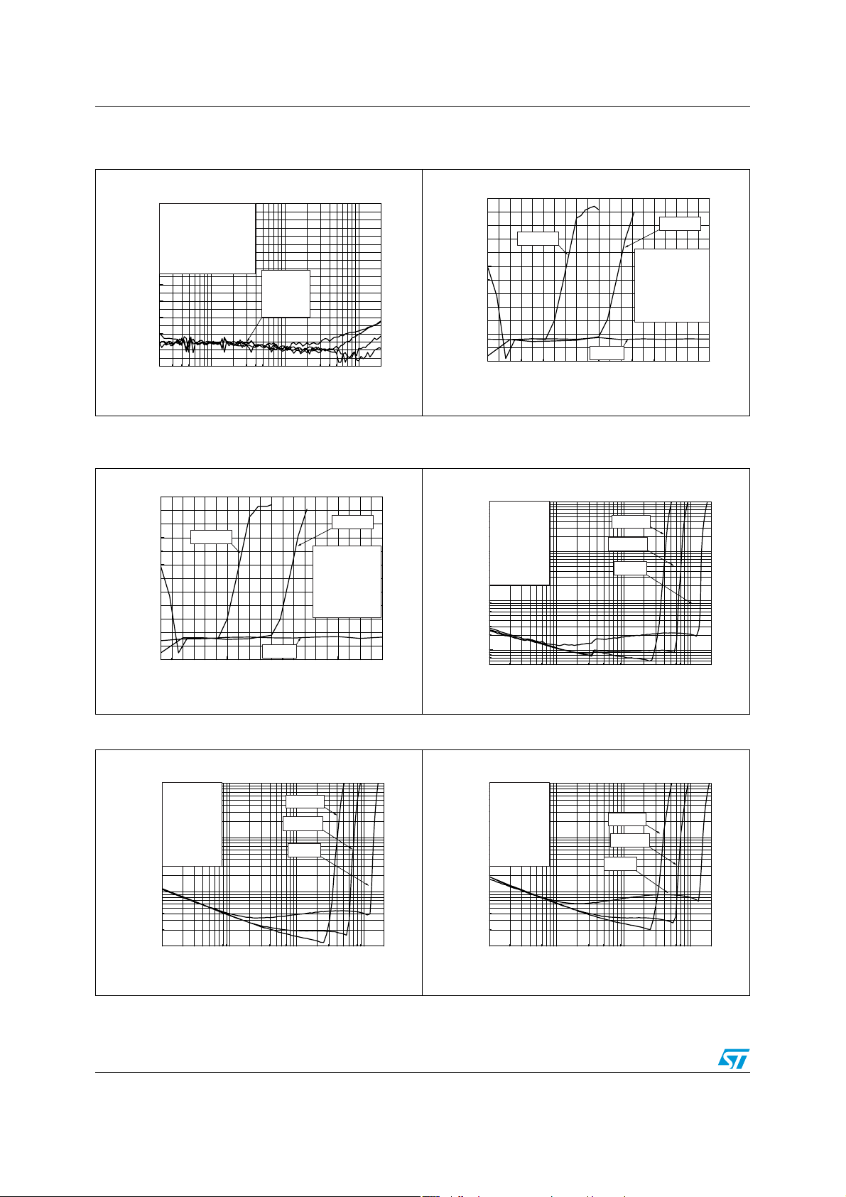
Electrical characteristics TS4994FC
0.0 0.5 1.0 1.5 2.0 2.5 3.0 3.5 4.0 4.5 5.0
-100
-80
-60
-40
-20
0
Vcc=3.3V
Vcc=2.5V
Vcc=5V
Vic = 200mVpp
F = 217Hz
Av = 1, Cb = 1μF
RL ≥ 8Ω
Tamb = 25°C
CMRR(dB)
Common Mode Input Voltage (V)
1E-3 0.01 0.1 1
0.01
0.1
1
10
Vcc=5V
Vcc=3.3V
Vcc=2.6V
RL = 4
Ω
F = 20Hz
Av = 1
Cb = 1μF
BW < 125kHz
Tamb = 25°C
THD + N (%)
Output Power (W)
1E-3 0.01 0.1 1
0.01
0.1
1
10
Vcc=5V
Vcc=3.3V
Vcc=2.6V
RL = 4
Ω
F = 20Hz
Av = 7.5
Cb = 1μF
BW < 125kHz
Tamb = 25°C
THD + N (%)
Output Power (W)
Figure 38. CMRR vs. frequency Figure 39. CMRR vs. common mode input
voltage
0
Vcc = 2.6V
-10
Vic = 200mVpp
-20
Av = 2.5, Cin = 470μF
RL ≥ 8
Tamb = 25°C
20
Ω
Cb=1μF
Cb=0.47μF
Cb=0.1μF
Cb=0
100 1000 10000
Frequency (Hz)
20k
Figure 41. THD+N vs. output power
-30
-40
-50
-60
CMRR (dB)
-70
-80
-90
-100
Figure 40. CMRR vs. common mode input
voltage
CMRR(dB)
-20
-40
-60
-80
0
Vcc=2.5V
Vcc=3.3V
Vic = 200mVpp
F = 217Hz
Av = 1, Cb = 0
RL ≥ 8Ω
Tamb = 25°C
-100
0.0 0.5 1.0 1.5 2.0 2.5 3.0 3.5 4.0 4.5 5.0
Common Mode Input Voltage (V)
Vcc=5V
Figure 42. THD+N vs. output power Figure 43. THD+N vs. output power
10
RL = 4
Ω
F = 20Hz
Av = 2.5
Cb = 1μF
1
BW < 125kHz
Tamb = 25°C
THD + N (%)
0.1
0.01
1E-3 0.01 0.1 1
14/35
Output Power (W)
Vcc=2.6V
Vcc=3.3V
Vcc=5V
Page 15
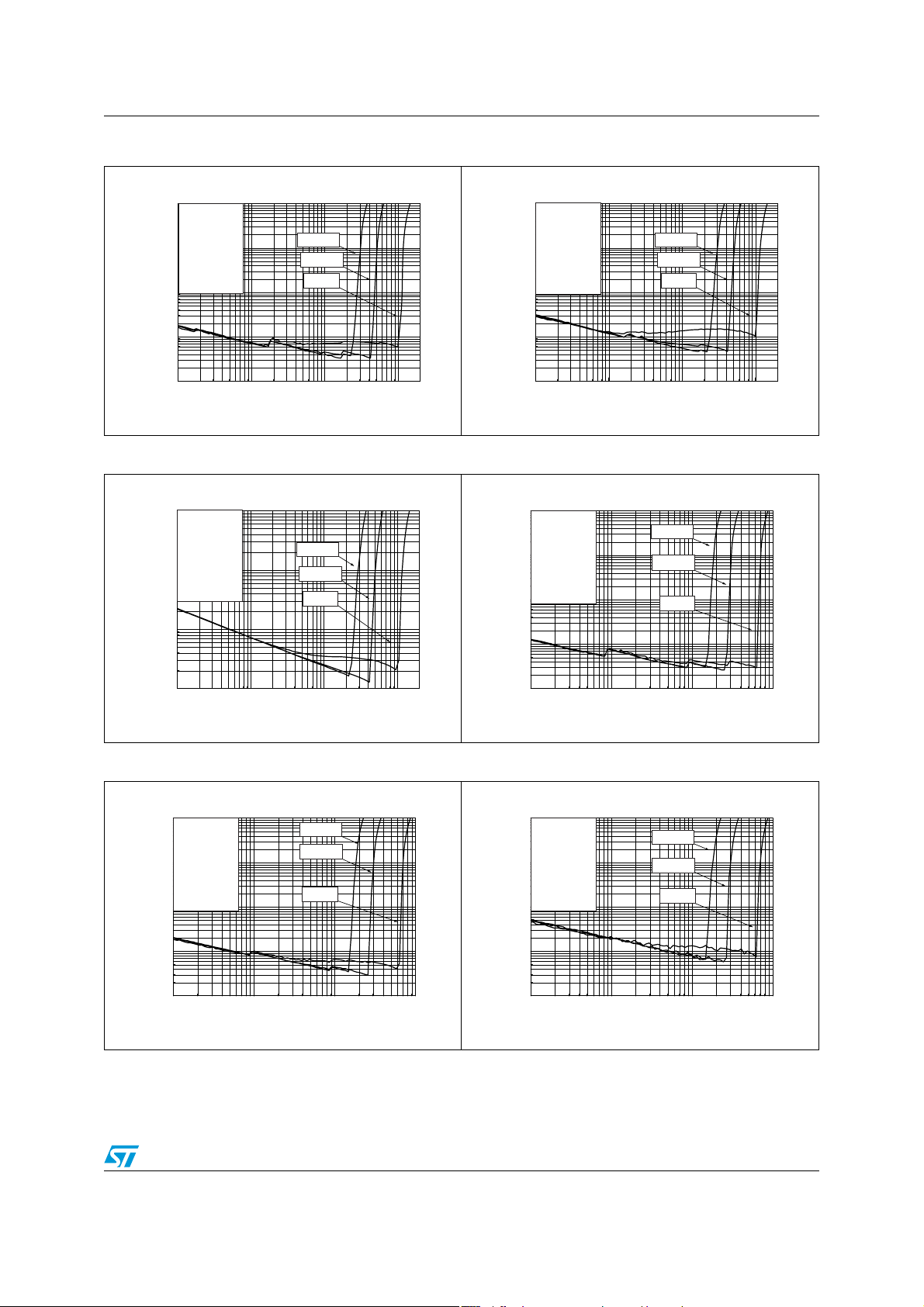
TS4994FC Electrical characteristics
1E-3 0.01 0.1 1
1E-3
0.01
0.1
1
10
Vcc=5V
Vcc=3.3V
Vcc=2.6V
RL = 8
Ω
F = 20Hz
Av = 2.5
Cb = 1μF
BW < 125kHz
Tamb = 25°C
THD + N (%)
Output Power (W)
1E-3 0.01 0.1 1
1E-3
0.01
0.1
1
10
Vcc=5V
Vcc=3.3V
Vcc=2.6V
RL = 16
Ω
F = 20Hz
Av = 1
Cb = 1μF
BW < 125kHz
Tamb = 25°C
THD + N (%)
Output Power (W)
1E-3 0.01 0.1 1
1E-3
0.01
0.1
1
10
Vcc=5V
Vcc=3.3V
Vcc=2.6V
RL = 16
Ω
F = 20Hz
Av = 7.5
Cb = 1μF
BW < 125kHz
Tamb = 25°C
THD + N (%)
Output Power (W)
Figure 44. THD+N vs. output power Figure 45. THD+N vs. output power
10
RL = 8
Ω
F = 20Hz
Av = 1
1
Cb = 1μF
BW < 125kHz
Tamb = 25°C
0.1
Vcc=2.6V
Vcc=3.3V
Vcc=5V
THD + N (%)
0.01
1E-3
1E-3 0.01 0.1 1
Output Power (W)
Figure 46. THD+N vs. output power Figure 47. THD+N vs. output power
10
RL = 8
Ω
1
THD + N (%)
0.1
F = 20Hz
Av = 7.5
Cb = 1μF
BW < 125kHz
Tamb = 25°C
Vcc=2.6V
Vcc=3.3V
Vcc=5V
0.01
1E-3 0.01 0.1 1
Output Power (W)
Figure 48. THD+N vs. output power Figure 49. THD+N vs. output power
10
RL = 16
Ω
F = 20Hz
Av = 2.5
1
Cb = 1μF
BW < 125kHz
Tamb = 25°C
0.1
THD + N (%)
0.01
1E-3
1E-3 0.01 0.1 1
Output Power (W)
Vcc=2.6V
Vcc=3.3V
Vcc=5V
15/35
Page 16
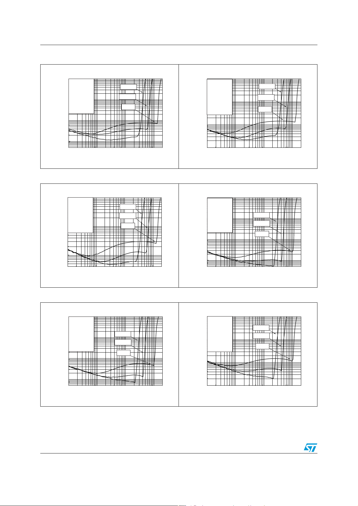
Electrical characteristics TS4994FC
1E-3 0.01 0.1 1
0.01
0.1
1
10
Vcc=5V
Vcc=3.3V
Vcc=2.6V
RL = 4
Ω
F = 1kHz
Av = 2.5
Cb = 1μF
BW < 125kHz
Tamb = 25°C
THD + N (%)
Output Power (W)
1E-3 0.01 0.1 1
0.01
0.1
1
10
Vcc=5V
Vcc=3.3V
Vcc=2.6V
RL = 8
Ω
F = 1kHz
Av = 1
Cb = 1μF
BW < 125kHz
Tamb = 25°C
THD + N (%)
Output Power (W)
1E-3 0.01 0.1 1
0.01
0.1
1
10
Vcc=5V
Vcc=3.3V
Vcc=2.6V
RL = 8
Ω
F = 1kHz
Av = 7.5
Cb = 1μF
BW < 125kHz
Tamb = 25°C
THD + N (%)
Output Power (W)
Figure 50. THD+N vs. output power Figure 51. THD+N vs. output power
10
RL = 4
1
THD + N (%)
0.1
Ω
F = 1kHz
Av = 1
Cb = 1μF
BW < 125kHz
Tamb = 25°C
Vcc=2.6V
Vcc=3.3V
Vcc=5V
0.01
1E-3 0.01 0.1 1
Output Power (W)
Figure 52. THD+N vs. output power Figure 53. THD+N vs. output power
10
RL = 4
F = 1kHz
Av = 7.5
Cb = 1μF
BW < 125kHz
1
Tamb = 25°C
Ω
Vcc=2.6V
Vcc=3.3V
Vcc=5V
THD + N (%)
0.1
1E-3 0.01 0.1 1
Output Power (W)
Figure 54. THD+N vs. output power Figure 55. THD+N vs. output power
10
RL = 8
Ω
F = 1kHz
Av = 2.5
Cb = 1μF
1
BW < 125kHz
Tamb = 25°C
THD + N (%)
0.1
0.01
1E-3 0.01 0.1 1
Vcc=2.6V
Vcc=3.3V
Vcc=5V
Output Power (W)
16/35
Page 17
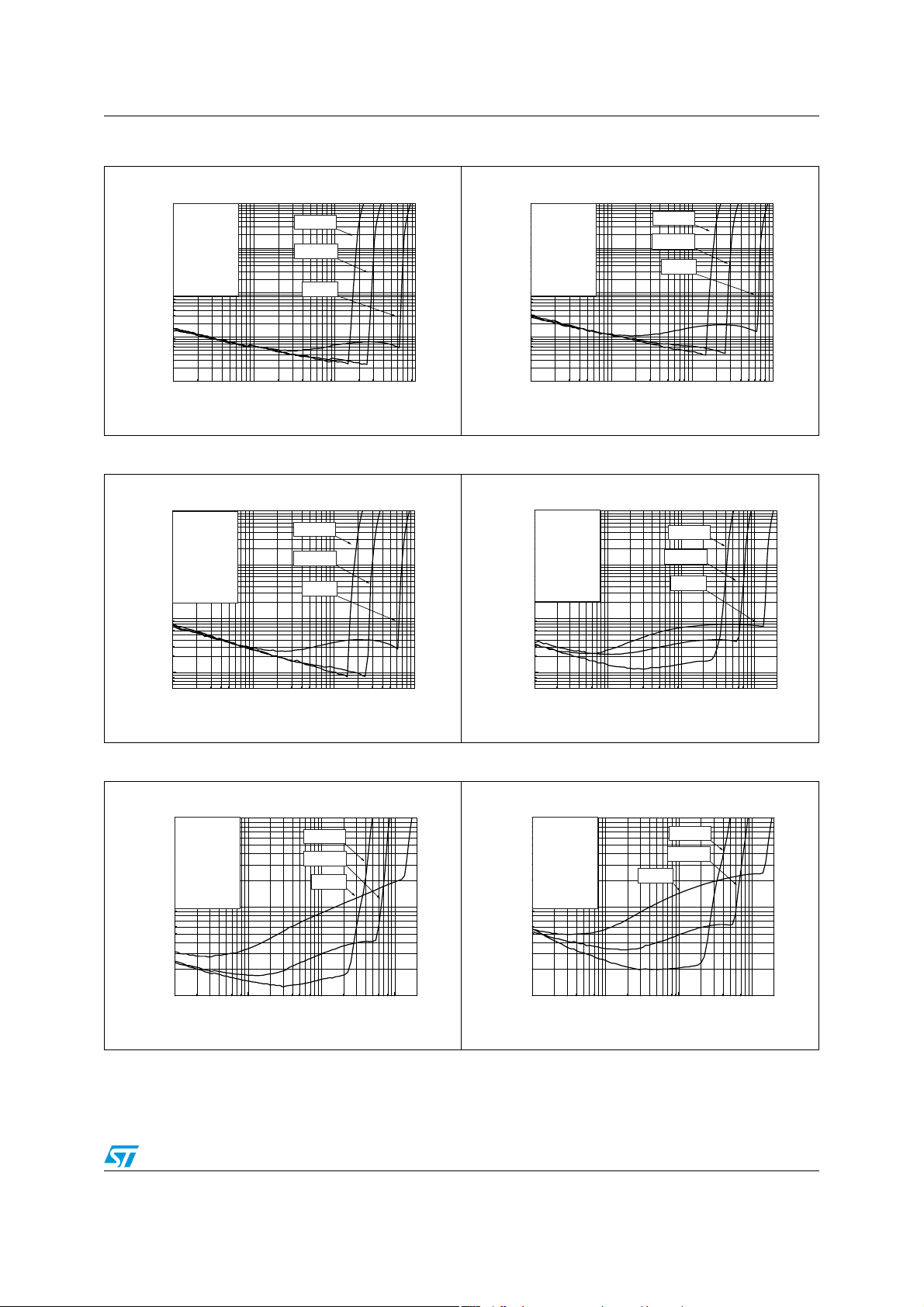
TS4994FC Electrical characteristics
1E-3 0.01 0.1 1
1E-3
0.01
0.1
1
10
Vcc=5V
Vcc=3.3V
Vcc=2.6V
RL = 16
Ω
F = 1kHz
Av = 2.5
Cb = 1μF
BW < 125kHz
Tamb = 25°C
THD + N (%)
Output Power (W)
1E-3 0.01 0.1 1
0.01
0.1
1
10
Vcc=5V
Vcc=3.3V
Vcc=2.6V
RL = 4
Ω
F = 20kHz
Av = 1
Cb = 1μF
BW < 125kHz
Tamb = 25°C
THD + N (%)
Output Power (W)
1E-3 0.01 0.1 1
0.1
1
10
Vcc=5V
Vcc=3.3V
Vcc=2.6V
RL = 4
Ω
F = 20kHz
Av = 7.5
Cb = 1μF
BW < 125kHz
Tamb = 25°C
THD + N (%)
Output Power (W)
Figure 56. THD+N vs. output power Figure 57. THD+N vs. output power
10
RL = 16
F = 1kHz
Av = 1
1
Cb = 1μF
BW < 125kHz
Tamb = 25°C
0.1
Ω
Vcc=2.6V
Vcc=3.3V
Vcc=5V
THD + N (%)
0.01
1E-3
1E-3 0.01 0.1 1
Output Power (W)
Figure 58. THD+N vs. output power Figure 59. THD+N vs. output power
10
RL = 16
F = 1kHz
Av = 7.5
Cb = 1μF
1
BW < 125kHz
Tamb = 25°C
Ω
Vcc=2.6V
Vcc=3.3V
Vcc=5V
THD + N (%)
0.1
0.01
1E-3 0.01 0.1 1
Output Power (W)
Figure 60. THD+N vs. output power Figure 61. THD+N vs. output power
10
RL = 4
Ω
F = 20kHz
Av = 2.5
Cb = 1μF
BW < 125kHz
Tamb = 25°C
1
THD + N (%)
0.1
1E-3 0.01 0.1 1
Output Power (W)
Vcc=2.6V
Vcc=3.3V
Vcc=5V
17/35
Page 18
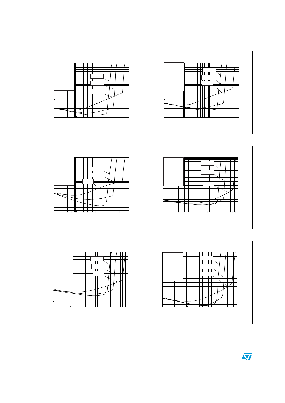
Electrical characteristics TS4994FC
1E-3 0.01 0.1 1
0.1
1
10
Vcc=5V
Vcc=3.3V
Vcc=2.6V
RL = 8
Ω
F = 20kHz
Av = 2.5
Cb = 1μF
BW < 125kHz
Tamb = 25°C
THD + N (%)
Output Power (W)
1E-3 0.01 0.1 1
0.01
0.1
1
10
Vcc=5V
Vcc=3.3V
Vcc=2.6V
RL = 16
Ω
F = 20kHz
Av = 1
Cb = 1μF
BW < 125kHz
Tamb = 25°C
THD + N (%)
Output Power (W)
Figure 62. THD+N vs. output power Figure 63. THD+N vs. output power
10
RL = 8
Ω
F = 20kHz
Av = 1
Cb = 1μF
BW < 125kHz
1
Tamb = 25°C
Vcc=2.6V
Vcc=3.3V
Vcc=5V
THD + N (%)
0.1
1E-3 0.01 0.1 1
Output Power (W)
Figure 64. THD+N vs. output power Figure 65. THD+N vs. output power
10
RL = 8
Ω
F = 20kHz
Av = 7.5
Cb = 1μF
BW < 125kHz
Tamb = 25°C
1
Vcc=2.6V
Vcc=3.3V
Vcc=5V
THD + N (%)
0.1
1E-3 0.01 0.1 1
Output Power (W)
Figure 66. THD+N vs. output power Figure 67. THD+N vs. output power
10
RL = 16
F = 20kHz
Av = 2.5
Cb = 1μF
1
BW < 125kHz
Tamb = 25°C
Ω
Vcc=2.6V
Vcc=3.3V
Vcc=5V
THD + N (%)
0.1
0.01
1E-3 0.01 0.1 1
Output Power (W)
10
RL = 16
F = 20kHz
Av = 7.5
Cb = 1μF
BW < 125kHz
Tamb = 25°C
1
Ω
Vcc=2.6V
Vcc=3.3V
Vcc=5V
THD + N (%)
0.1
1E-3 0.01 0.1 1
Output Power (W)
18/35
Page 19
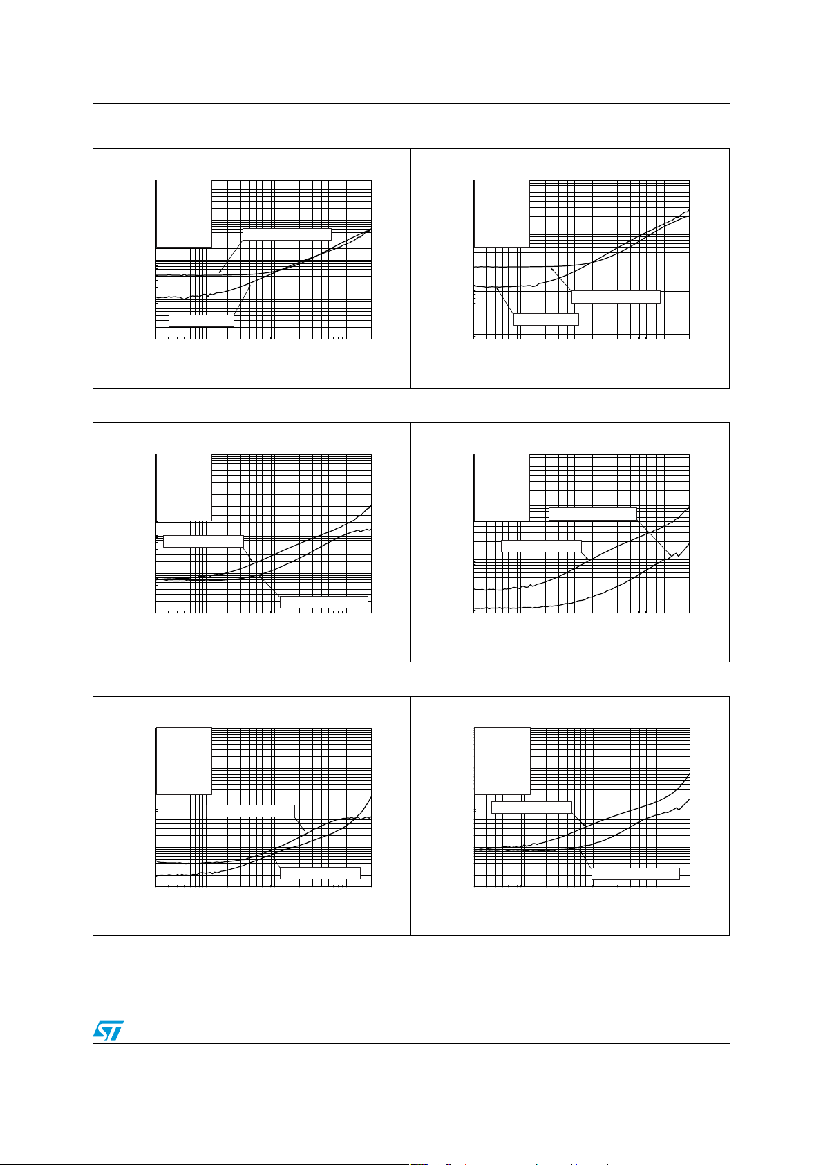
TS4994FC Electrical characteristics
100 1000 10000
0.01
0.1
1
10
Vcc=2.6V, Po=350mW
Vcc=5V, Po=1W
RL = 4
Ω
Av = 7.5
Cb = 1μF
Bw < 125kHz
Tamb = 25°C
20k20
THD + N (%)
Frequency (Hz)
100 1000 10000
0.01
0.1
1
10
Vcc=2.6V, Po=225mW
Vcc=5V, Po=850mW
RL = 8
Ω
Av = 7.5
Cb = 1μF
Bw < 125kHz
Tamb = 25°C
20k20
THD + N (%)
Frequency (Hz)
100 1000 10000
1E-3
0.01
0.1
1
10
Vcc=2.6V, Po=155mW
Vcc=5V, Po=600mW
RL = 16
Ω
Av = 7.5
Cb = 1μF
Bw < 125kHz
Tamb = 25°C
20k20
THD + N (%)
Frequency (Hz)
Figure 68. THD+N vs. frequency Figure 69. THD+N vs. frequency
10
RL = 4
Ω
Av = 1
Cb = 1μF
1
Bw < 125kHz
Tamb = 25°C
Vcc=2.6V, Po=350mW
0.1
THD + N (%)
0.01
Vcc=5V, Po=1W
1E-3
100 1000 10000
20k20
Frequency (Hz)
Figure 70. THD+N vs. frequency Figure 71. THD+N vs. frequency
10
RL = 8
Ω
Av = 1
Cb = 1μF
1
Bw < 125kHz
Tamb = 25°C
0.1
Vcc=5V, Po=850mW
THD + N (%)
0.01
1E-3
100 1000 10000
Vcc=2.6V, Po=225mW
20k20
Frequency (Hz)
Figure 72. THD+N vs. frequency Figure 73. THD+N vs. frequency
10
RL = 16
Ω
Av = 1
Cb = 1μF
1
Bw < 125kHz
Tamb = 25°C
0.1
THD + N (%)
0.01
1E-3
Vcc=2.6V, Po=155mW
Vcc=5V, Po=600mW
100 1000 10000
Frequency (Hz)
20k20
19/35
Page 20
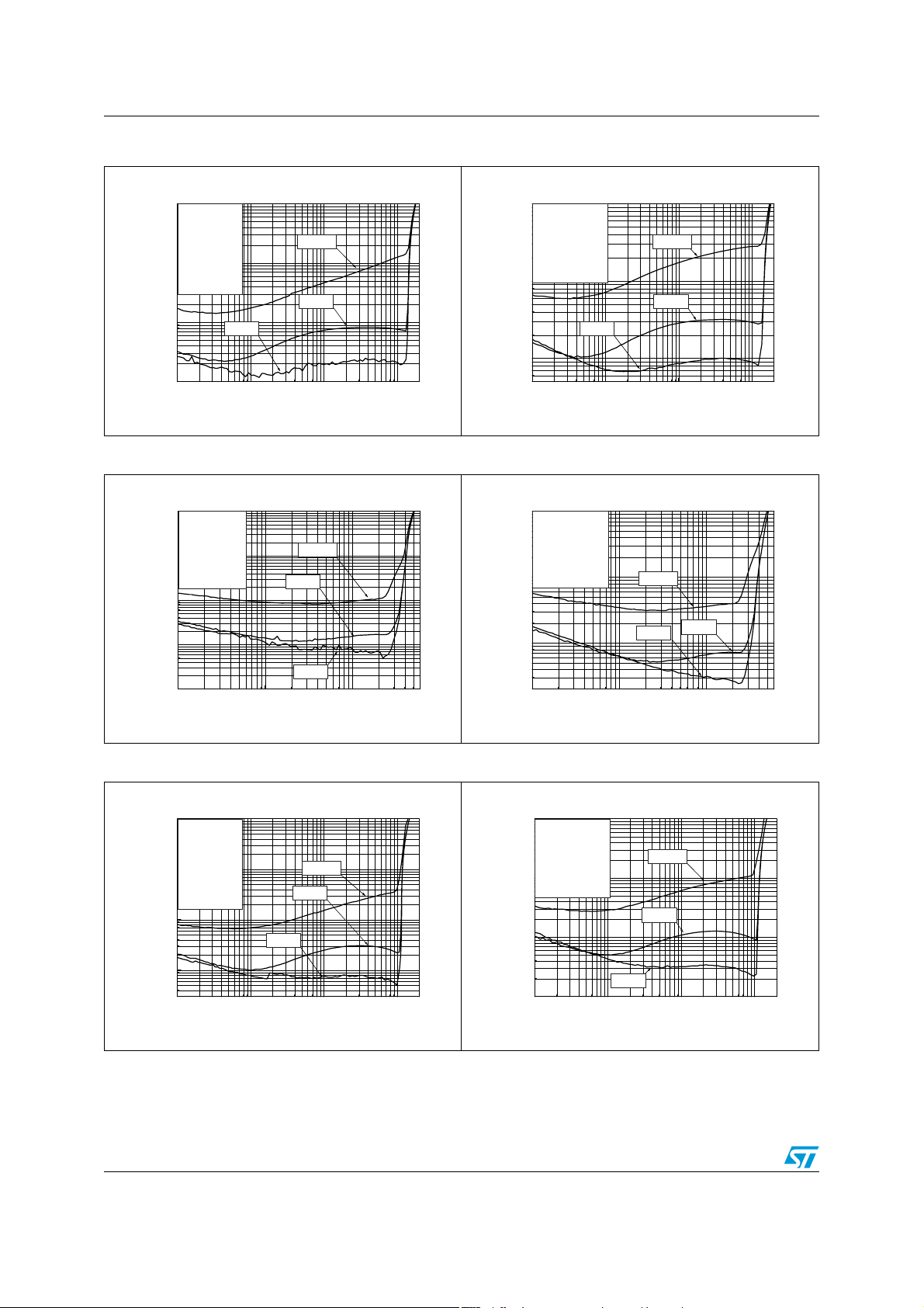
Electrical characteristics TS4994FC
1E-3 0.01 0.1 1
0.1
1
10
F=20kHz
F=20Hz
F=1kHz
RL = 4
Ω
Vcc = 5V
Av = 7.5, Cb = 0
BW < 125kHz
Tamb = 25°C
THD + N (%)
Output Power (W)
1E-3 0.01 0.1
0.1
1
10
F=20kHz
F=20Hz
F=1kHz
RL = 4
Ω
Vcc = 2.6V
Av = 7.5, Cb = 0
BW < 125kHz
Tamb = 25°C
THD + N (%)
Output Power (W)
1E-3 0.01 0.1 1
0.01
0.1
1
10
F=20kHz
F=20Hz
F=1kHz
RL = 8
Ω
Vcc = 5V
Av = 7.5, Cb = 0
BW < 125kHz
Tamb = 25°C
THD + N (%)
Output Power (W)
Figure 74. THD+N vs. output power Figure 75. THD+N vs. output power
10
RL = 4
Ω
Vcc = 5V
Av = 1
Cb = 0
1
BW < 125kHz
Tamb = 25°C
THD + N (%)
0.1
0.01
1E-3 0.01 0.1 1
F=20Hz
F=20kHz
F=1kHz
Output Power (W)
Figure 76. THD+N vs. output power Figure 77. THD+N vs. output power
10
RL = 4
Ω
1
0.1
THD + N (%)
Vcc = 2.6V
Av = 1, Cb = 0
BW < 125kHz
Tamb = 25°C
F=20kHz
F=1kHz
0.01
1E-3
1E-3 0.01 0.1
Figure 78. THD+N vs. output power Figure 79. THD+N vs. output power
10
RL = 8
Ω
Vcc = 5V
Av = 1
1
Cb = 0
BW < 125kHz
Tamb = 25°C
0.1
THD + N (%)
0.01
1E-3 0.01 0.1 1
20/35
F=20Hz
Output Power (W)
F=20kHz
F=1kHz
F=20Hz
Output Power (W)
Page 21
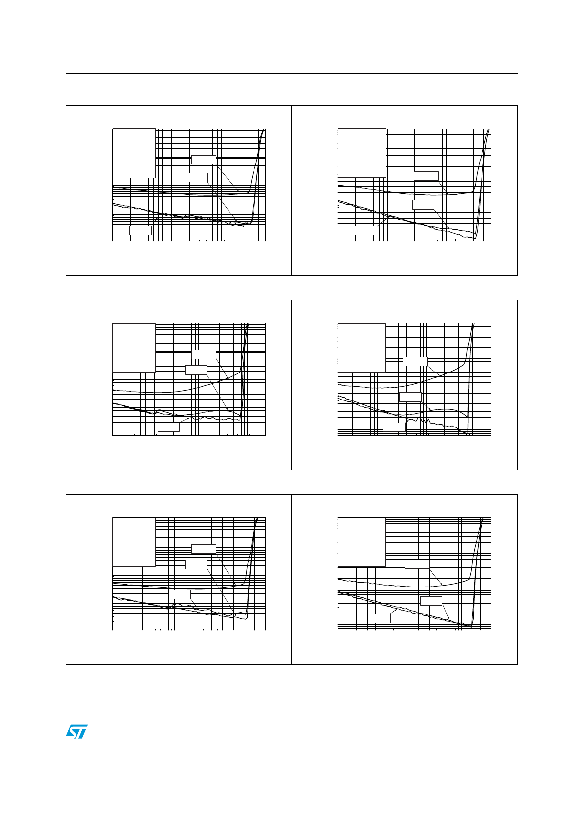
TS4994FC Electrical characteristics
1E-3 0.01 0.1
0.01
0.1
1
10
F=20kHz
F=20Hz
F=1kHz
RL = 8
Ω
Vcc = 2.6V
Av = 7.5, Cb = 0
BW < 125kHz
Tamb = 25°C
THD + N (%)
Output Power (W)
1E-3 0.01 0.1 1
0.01
0.1
1
10
F=20kHz
F=20Hz
F=1kHz
RL = 16
Ω
Vcc = 5V
Av = 7.5, Cb = 0
BW < 125kHz
Tamb = 25°C
THD + N (%)
Output Power (W)
1E-3 0.01 0.1
0.01
0.1
1
10
F=20kHz
F=20Hz
F=1kHz
RL = 16
Ω
Vcc = 2.6V
Av = 7.5, Cb = 0
BW < 125kHz
Tamb = 25°C
THD + N (%)
Output Power (W)
Figure 80. THD+N vs. output power Figure 81. THD+N vs. output power
10
RL = 8
Ω
Vcc = 2.6V
Av = 1, Cb = 0
1
BW < 125kHz
Tamb = 25°C
0.1
F=20kHz
F=1kHz
THD + N (%)
0.01
F=20Hz
1E-3
1E-3 0.01 0.1
Output Power (W)
Figure 82. THD+N vs. output power Figure 83. THD+N vs. output power
10
RL = 16
Ω
Vcc = 5V
Av = 1, Cb = 0
1
0.1
THD + N (%)
BW < 125kHz
Tamb = 25°C
F=20kHz
F=1kHz
0.01
1E-3
1E-3 0.01 0.1 1
F=20Hz
Output Power (W)
Figure 84. THD+N vs. output power Figure 85. THD+N vs. output power
10
RL = 16
Ω
Vcc = 2.6V
Av = 1, Cb = 0
1
BW < 125kHz
Tamb = 25°C
0.1
THD + N (%)
0.01
1E-3
1E-3 0.01 0.1
Output Power (W)
F=20kHz
F=1kHz
F=20Hz
21/35
Page 22
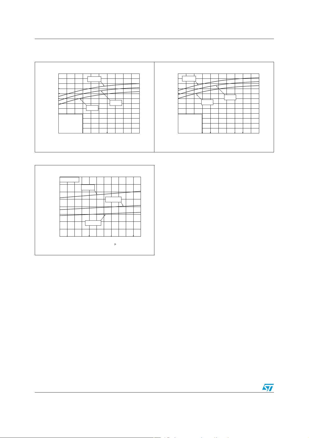
Electrical characteristics TS4994FC
2.5 3.0 3.5 4.0 4.5 5.0
80
85
90
95
100
105
110
Av = 2.5
Cb = 1μF
THD+N < 0.7%
Tamb = 25°C
RL=16
Ω
RL=4
Ω
RL=8
Ω
Signal to Noise Ratio (dB)
Power Supply Voltage (V)
Figure 86. SNR vs. power supply voltage with
unweighted filter
110
RL=16
RL=4
Ω
RL=8
Ω
Ω
105
100
95
90
Av = 2.5
Signal to Noise Ratio (dB)
Cb = 1μF
85
THD+N < 0.7%
Tamb = 25°C
80
2.5 3.0 3.5 4.0 4.5 5.0
Power Supply Voltage (V)
Figure 88. Startup time vs. bypass capacitor
20
Tamb=25°C
15
10
Vcc=5V
Vcc=3.3V
Figure 87. SNR vs. power supply voltage with
A-weighted filter
Startup Time (ms)
5
0
0.0 0.4 0.8 1.2 1.6 2.0
Vcc=2.6V
Bypass Capacitor Cb ( F)
22/35
Page 23

TS4994FC Application information
4 Application information
4.1 Differential configuration principle
The TS4994 is a monolithic full-differential input/output power amplifier. The TS4994 also
includes a common mode feedback loop that controls the output bias value to average it at
V
/2 for any DC common mode input voltage. This allows the device to always have a
CC
maximum output voltage swing, and by co nsequence, maximize the output power.
Moreover, as the load is connected differentially, compared to a single-ended topology, the
output is four times higher for the same power supply voltage.
The advantages of a full-differential amplifier are:
● Very high PSRR (power supply rejection ratio).
● High common mode noise rejection.
● Virtually zero pop without additional circuitry, giving a faster start-up time compared
with conventional single-ended input amplifiers.
● Easier interfacing with differential output audio DAC.
● No input coupling capacitors required due to common mode feedback loop.
● In theory, the filtering of the internal bias by an external bypass capacitor is not
necessary . Bu t, to reach maximum performance in all tolerance situations , it is better to
keep this option.
The main disadvantage is:
● As the differential function is directly linked to the mismatch between external resistors,
paying particular attention to this mismatch is mandatory in order to get the best
performance from the amplifier.
4.2 Gain in typical application schematic
A typical differential application is shown in Figure 1 on page 3.
In the flat region of the frequency-response curve (no C
effect), the differential gain is
in
expressed by the relation:
R
feed
--------------==
R
where R
in
= R
in1
= R
and R
in2
Note: For the rest of this section, Av
VO+VO–
A
------------------------------------------------------
V
diff
Diff
input+
= R
feed
diff
feed1
will be called AV to simplify the expression.
= R
–
feed2
Diff
input-
.
4.3 Common mode feedback loop limitations
As explained pre viously, the common mode feedback loop allows the output DC bias voltage
to be averaged at V
However, due to V
mode feedback loop can play its role only within a defined rang e. This range depends upon
/2 for any DC common mode bias input voltage.
CC
limitation of the input stage (see Table 3 on page 5), the common
ICM
in
23/35
Page 24

Application information TS4994FC
the values of VCC, Rin and R
(AV). To have a good estimation of the V
feed
following formula:
V
× 2VicR
CCRin
V
------------------------------------------------------------------------- -
ICM
2R
+()×
inRfeed
with
Diff
input+
------------------------------------------------------ -
V
ic
+
2
Diff
input-
The result of the calculation must be in the range:
If the result of the V
0.6V V
calculation is not in this range, an input coupling capacitor must be
ICM
ICMVCC
used.
Example: With V
=2.5V, Rin=R
CC
= 20k and Vic= 2V, we find V
feed
higher than 2.5V- 0.9V = 1.6V, so input coupling capacitors are required. Alternatively, you
can change the V
value.
ic
4.4 Low and high frequency response
In the low frequency region, Cin starts to have an effect. Cin forms, with Rin, a high-pass filter
with a -3dB cut-off frequency. F
is in Hz.
CL
F
CL
=
1
CR2
××π×
value, use the
ICM
××+
feed
(V)=
(V)=
0.9V–≤≤
= 1.63V. This is
ICM
)Hz(
inin
In the high-frequency region, you can limit the bandwidth by adding a capacitor (C
parallel with R
. It forms a low-pass filter with a -3dB cut-of f frequency. FCH is in Hz.
feed
=
F
CH
1
××π×
CR2
feedfeed
)Hz(
feed
) in
While these bandwidth limitations are in theory attractive, in practice, because of low
performance in terms of capacitor precision (and by consequen ce in terms of mismatching),
they deteriorate the values of PSRR and CMRR.
The influence of mismatching on PSRR and CMRR performance is discussed in more detail
in the following sections.
Example: A typical application with input coupling and feedback capacitor with F
and F
= 8kHz. We assume that the mismatching between R
CH
in1,2
and C
feed1,2
=50Hz
CL
can be
neglected. If we sweep the frequency from DC to 20kHz we observe the following with
respect to the PSRR value:
● From DC to 200Hz, the C
C
impedance is high enough to be neglected. Due to the tolerance of C
feed
impedance decreases from infinite to a finite value and the
in
in1,2
, we
24/35
Page 25

TS4994FC Application information
must introduce a mismatch fa ctor (R
in1xCin
≠ R
in2xCin2
) that will decrease the PSRR
performance.
● From 200Hz to 5kHz, the C
compared with R
and the C
in,
impedance is low enough to be neglected when
in
impedance is high enough to be neglected as well. In
feed
this range, we can reach the PSRR performance of the TS4994 itself.
● From 5kHz to 20kHz, the C
and the C
impedance decreases to a finite value. Due to tolerance of C
feed
introduce a mismatching factor (R
impedance is low to be neglected when compared to R
in
feed1xCfeed1
≠ R
feed2xCfeed2
) that will decrease the
PSRR performance.
4.5 Calculating the influence of mismatching on PSRR performance
For calculating PSRR performance, we consider that Cin and C
use the same kind of resistor (same tolerance) and ΔR is the tolerance value in %.
The following PSRR equation is valid for frequencies ranging from DC to about 1kHz.
The PSRR equation is (ΔR in %):
⎡
×≤
Log20PSRR
×Δ
⎢
⎣
⎤
100R
⎥
2
Δ−
)R10000(
⎦
This equation doesn't include the additional performance provided by bypass capacitor
filtering. If a bypass capacitor is added, it acts, together with the internal high output
impedance bias, as a low-pass filter, and the result is a quite important PSRR improvement
with a relatively small bypass capacitor.
have no influence. We
feed
)dB(
feed1,2
, we
in,
The complete PSRR equation (ΔR in %, C
PSRR 20 log ×≤
Example: With ΔR = 0.1% and C
--------------------------------------------------------------------------------------------------------(1000 R
= 0, the minimum PSRR is -60dB. With a 100nF bypass
b
in microFarad and F in Hz) is:
b
R 100×Δ
2
) 1F
2
2
C
b
dB()
22.2××+×Δ–
capacitor, at 100Hz the new PSRR would be -93dB.
This example is a worst case scenario, where each resistor has extreme tolerance. It
illustrates the fact that with only a small bypass capacitor, the TS4994 provides high PSRR
performance.
Note also that this is a theoretical formula. Because the TS4994 has self-generated noise,
you should consider that the highest practical PSRR reachable is about -110dB. It is
therefore unreasonable to target a -120dB PSRR.
25/35
Page 26
Application information TS4994FC
100 1000 10000
-140
-130
-120
-110
-100
-90
-80
-70
-60
-50
-40
-30
-20
-10
0
Cb=0.1μF
Cb=1μF
Cb=0
20k
20
Cb=0.47μF
Vcc = 3.3V, Vripple = 200mVpp
Av = 1, Cin = 4.7μF
Δ
R/R = 0.1%, RL ≥ 8
Ω
Tamb = 25°C, Inputs = Grounded
PSRR (dB)
Frequency (Hz)
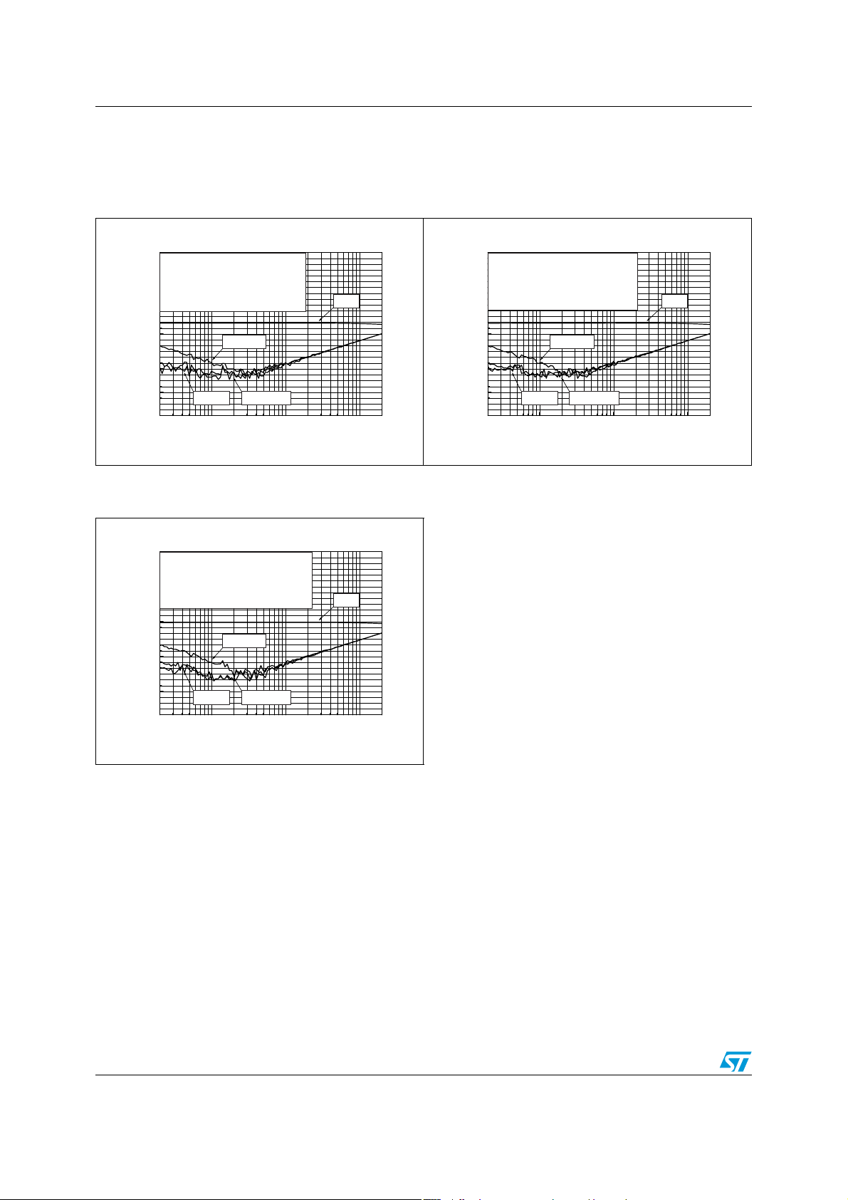
The three following g raphs show PSRR v ersus frequency and v ersus b ypass capacitor Cb in
worst-case conditions (
Figure 89. PSRR vs. frequency (worst case
conditions)
0
-10
Vcc = 5V, Vripple = 200mVpp
-20
Av = 1, Cin = 4.7μF
-30
Δ
R/R = 0.1%, RL ≥ 8
-40
Tamb = 25°C, Inputs = Grounded
-50
-60
-70
-80
PSRR (dB)
-90
-100
-110
-120
-130
-140
Cb=1μF
20
100 1000 10000
Ω
Cb=0.1μF
Cb=0.47μF
Frequency (Hz)
Δ
R = 0.1%).
Cb=0
Figure 90. PSRR vs. frequency (worst case
conditions)
20k
Figure 91. PSRR vs. frequency (worst case
conditions)
0
-10
Vcc = 2.5V, Vripple = 200mVpp
-20
Av = 1, Cin = 4.7μF
-30
Δ
R/R = 0.1%, RL ≥ 8
Tamb = 25°C, Inputs = Grounded
-40
-50
-60
-70
-80
PSRR (dB)
-90
-100
-110
-120
-130
-140
Cb=1μF
20
100 1000 10000
Ω
Cb=0.1μF
Cb=0.47μF
Frequency (Hz)
Cb=0
20k
26/35
Page 27
TS4994FC Application information
100 1000 10000
-140
-130
-120
-110
-100
-90
-80
-70
-60
-50
-40
-30
-20
-10
0
Cb=0.1μF
Cb=1μF
Cb=0
20k
20
Cb=0.47μF
Vcc = 2.5V, Vripple = 200mVpp
Av = 1, Cin = 4.7μF
Δ
R/R ≤ 0.1%, RL ≥ 8
Ω
Tamb = 25°C, Inputs = Grounded
PSRR (dB)
Frequency (Hz)
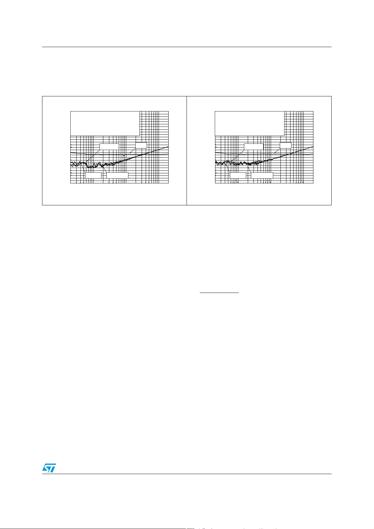
The two followin g graphs sho w typical applications of the TS4994 wit h a random selection of
four
Δ
R/R values with a 0.1% tolerance.
Figure 92. PSRR vs. frequency with random
choice condition
0
-10
Vcc = 5V, Vripple = 200mVpp
Av = 1, Cin = 4.7μF
-20
Δ
R/R ≤ 0.1%, RL ≥ 8
-30
Tamb = 25°C, Inputs = Grounded
-40
-50
-60
-70
-80
PSRR (dB)
-90
-100
-110
-120
-130
-140
Cb=1μF
20
100 1000 10000
Ω
Cb=0.1μF
Cb=0.47μF
Frequency (Hz)
Figure 93. PSRR vs. frequency with random
choice condition
Cb=0
20k
4.6 CMRR performance
For calculating CMRR performance, we consider that Cin and C
has no influence in the calculation of the CMRR.
We use the same kind of resistor (same tolerance) and ΔR is the tolerance value in %.
The following CMRR equation is valid for frequencies ranging from DC to about 1kHz.
The CMRR equation is (ΔR in %):
Example: With ΔR = 1%, the minimum CMRR is -34dB.
This example is a worst case scenario where each resistor has extreme tolerance. Ut
illustrates the fact that for CMRR, good matching is essential.
As with the PSRR, due to self-generated noise, the TS4994 CMRR limitation is about
-110dB.
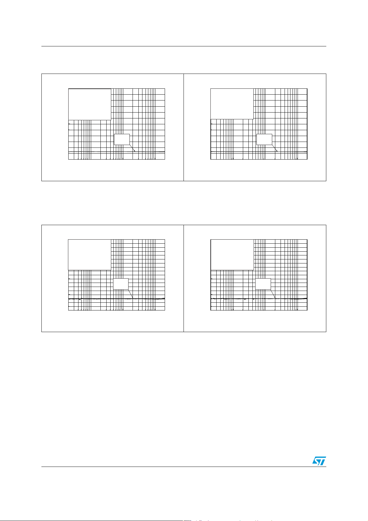
Figure 94 and Figure 95 show CMRR versus frequency and versus bypass capacitor C
worst-case conditions (ΔR=0.1%).
have no influence. Cb
feed
⎡
Log20CMRR
×≤
⎢
×Δ
⎣
⎤
200R
2
)R10000(
Δ−
)dB(
⎥
⎦
in
b
27/35
Page 28
Application information TS4994FC
100 1000 10000
-60
-50
-40
-30
-20
-10
0
Cb=1μF
Cb=0
20k
20
Vcc = 2.5V
Vic = 200mVpp
Av = 1, Cin = 470μF
Δ
R/R = 0.1%, RL ≥ 8
Ω
Tamb = 25°C
CMRR (dB)
Frequency (Hz)
100 1000 10000
-90
-80
-70
-60
-50
-40
-30
-20
-10
0
Cb=1μF
Cb=0
20k
20
Vcc = 2.5V
Vic = 200mVpp
Av = 1, Cin = 470μF
Δ
R/R ≤ 0.1%, RL ≥ 8
Ω
Tamb = 25°C
CMRR (dB)
Frequency (Hz)
Figure 94. CMRR vs. frequency (worst case
conditions)
0
Vcc = 5V
Vic = 200mVpp
-10
Av = 1, Cin = 470μF
Δ
-20
-30
CMRR (dB)
-40
-50
-60
Tamb = 25°C
20
R/R = 0.1%, RL ≥ 8
Ω
Cb=1μF
Cb=0
100 1000 10000
Frequency (Hz)
20k
Figure 96 and Figure 97 show CMRR versus frequency for a typical application with a
random selection of four
Δ
R/R values with a 0.1% tolerance.
Figure 96. CMRR vs. frequency with random
selection condition
Figure 95. CMRR vs. frequency (worst case
conditions)
Figure 97. CMRR vs. frequency with random
selection condition
0
Vcc = 5V
-10
Vic = 200mVpp
-20
Av = 1, Cin = 470μF
Δ
-30
-40
-50
CMRR (dB)
-60
-70
-80
-90
Tamb = 25°C
20
R/R ≤ 0.1%, RL ≥ 8
Ω
Cb=1μF
Cb=0
100 1000 10000
Frequency (Hz)
20k
4.7 Power dissipation and efficiency
Assumptions:
● Load voltage and current are sinusoidal (V
● Supply voltage is a pure DC source (V
The output voltage is:
V
out
= V
CC
)
peak
and I
out
sinωt (V)
out
)
and
28/35
I
out
=
V
out
------------ -
R
L
(A)
Page 29

TS4994FC Application information
and
2
V
peak
-------------------- -
P
out
=
2R
(W)
L
Therefore, the average current delivered by the supply voltag e is:
Equation 1
V
peak
---------------- -
AVG
= 2
I
CC
πR
(A)
L
The power delivered by the supply voltage is:
P
supplyVCCICC
AVG
(W)⋅=
Therefore, the power dissipated by each amplifier is:
P
diss
P
supplyPout
(W)–=
Equation 2
P
diss
----------------------
π R
L
–=
P
outPout
22V
CC
and the maximum value is obtained when:
∂P
diss
----------------- = 0
∂P
out
and its value is:
Equation 3
2
maxPdiss
Vcc2
=
π
)W(
2
R
L
Note: This maximum value is only dependent on the power supply voltage and load values.
The efficiency is the ratio between the output power and the power supply:
Equation 4
P
-------------------
η =
P
supply
The maximum theoretical value is reached when V
η =
out
π
---- -
= 78.5%
4
πV
--------------------
=
peak
peak
4V
CC
= VCC, so:
The maximum die temperature allowable for the TS4994 is 125°C. However, in case of
overheating, a thermal shutdown set to 150°C, puts the TS4994 in standby until the
temperature of the die is reduced by about 5°C.
29/35
Page 30

Application information TS4994FC
To calculate the maximum ambient temperature T
● The value of the power supply voltage, V
● The value of the load resistor, R
● The R
Example: V
value f or the package type
thja
=5V, RL=8Ω, R
CC
thja-flipchip
Using the power dissipation formula given above in Equation 3 this gives a result of:
P
T
is calculated as follows:
amb
dissmax
= 633mW
Equation 5
T
amb
Therefore, the maximum allowable value for T
T
= 125-80x0.633=62°C
amb
4.8 Decoupling of the circuit
Two capacitors are needed to correctly bypass the TS4994. A power supply bypass
capacitor C
C
has particular influence on the THD+N in the high frequency region (abov e 7kHz) and an
s
indirect influence on power supply disturbances. With a value for C
similar THD+N performance to that shown in the datasheet.
and a bias voltage bypass capacitor Cb.
s
allowable, you need to know:
amb
CC
L
= 100°C/W (100mm² copper heatsink)
125° CR
×–=
TJHAPdissmax
is:
amb
s
of 1µF, you can expect
In the high frequency region, if C
on the power supply rail are less filtered.
On the other hand, if C
more filtered.
C
has an influence on THD+N at lower frequencies, but its function is critical to the final
b
result of PSRR (with input grounded and in the lower frequency region).
4.9 Wake-up time: t
When the standby is released to put the device ON, the bypass capa cit or Cb is not charged
immediately. As C
properly until the C
time or t
and is specified in Table 3 on page 5, with Cb=1µF. During the wake-up time, the
WU
TS4994 gain is close to zero. After the wake-up time, the gain is released and set to its
nominal value.
If C
has a value other than 1µF, refer to the graph in Figure 88 on page 22 to establish the
b
wake-up time.
is directly linked to the bias of the amplifier, the bias will not work
b
voltage is correct. The time to reach this voltage is called the wake-up
b
is lower than 1µF, it increases THD+N, and disturbances
s
is higher than 1µF, the disturbances on the power supply rail are
s
WU
30/35
Page 31
TS4994FC Application information
−
4.10 Shutdown time
When the standby command is set, the time required to put the two output stages in high
impedance and the internal circuitry in shutdown mode is a few micr oseconds.
Note: In shutdown mode, the Bypass pin and Vin+, Vin- pins are short-circuited to ground by
internal switches. This allows a quick discharge of the C
and Cin capacitors.
b
4.11 Pop performance
Due to its fully differential structure, the pop performance of the TS4994 is close to perfect.
However, due to mismatching between internal resistors R
capacitors C
, some noise might remain at startup. To eliminate the effect of mismatched
in
, R
in
, and external input
feed
components, the TS4994 includes pop reduction circuitry . With this circuitry, the TS4994 is
close to zero pop for all possible common applications.
In addition, when the TS4994 is in standb y mode, due to the h igh impedance output stage in
this configuration, no pop is heard.
4.12 Single-ended input configuration
It is possible to use the TS4994 in a single-ended input configuration. However, input
coupling capacitors are needed in this configuration. The schematic in Figure 98 shows an
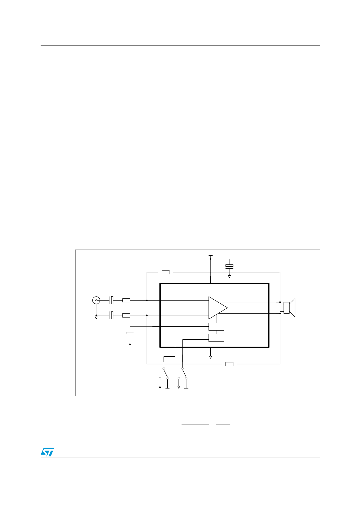
example of this configuration.
Figure 98. Single-ended input typical application
VCC
+
Cs
GND
Rfeed2
20k
1u
Vo+
5
Vo-
7
8 Ohms
Ve
GND
Cin1
220nF
Cin2
220nF
Rfeed1
20k
Rin1
+
20k
Rin2
+
20k
+
Cb
1u
GND
3
Vin-
1
Vin+
8
Bypass
Mode Stdby TS4994IJ
4
GND GNDVCC VCC
2
VCC
-
+
Bias
Standby
GND
69
GND
The component calculations remain the same, except for the gain. In single-ended input
configuration, the formula is:
R
=
Av =
SE
VV
Ve
feedOO
−+
R
in
31/35
Page 32
Package information TS4994FC
5 Package information
In order to meet environmental requirements, STMicroelectronics offers these devices in
ECOPACK
category of second level interconnect is marke d on the pa ckage and on the inner box label,
in compliance with JEDEC Standard JESD97. The maximum ratings related t o soldering
conditions are also marked on the inner box label. ECOPACK is an STMicroelectronics
trademark. ECOPACK specifications are available at: www.st.com
®
packages. These packages have a Lead-free second level interconnect. The
.
Flip-chip package (9 bumps)
Dimensions in millimeters unless otherwise indicated.
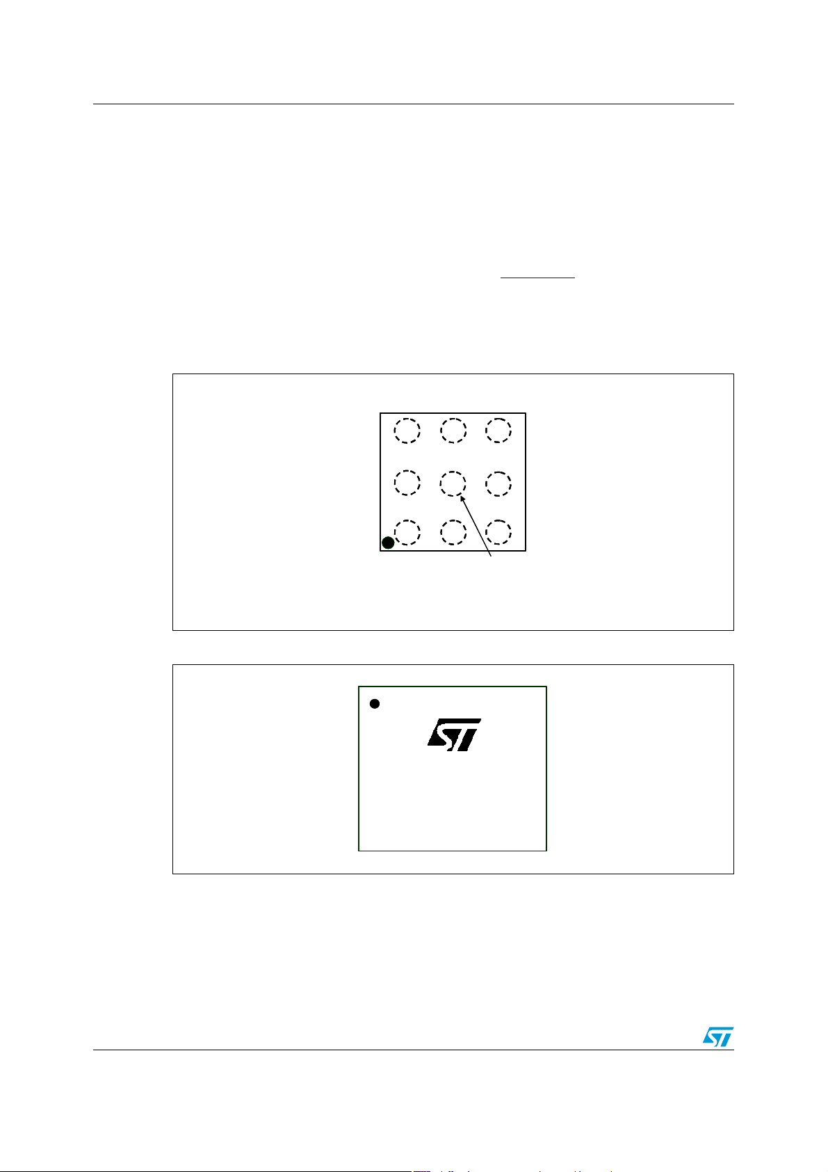
Figure 99. Pinout (top view)
Gnd
Gnd
V
V
O-
O-
Bypass Stdby
Bypass Stdby
V
V
IN+
IN+
765
765
9
8
8
1
1
9
2
2
V
V
CC
CC
V
V
O+
O+
4
4
V
V
3
3
Stdby Mode
Stdby Mode
IN-
IN-
* Balls are underneath
Figure 100. Marking (top view)
A94
A94
YWW
YWW
E
E
32/35
Page 33
TS4994FC Package information
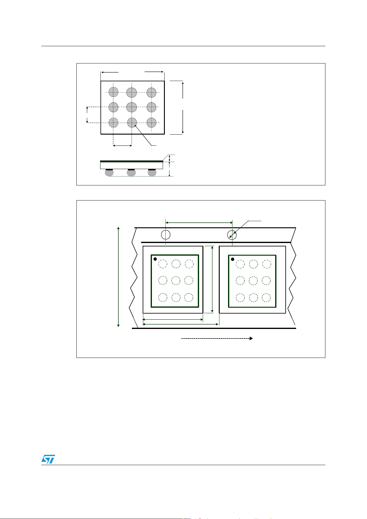
Figure 101. Dimensions
1.63 mm
1.63 mm
0.5mm
0.5mm
0.5mm
0.5mm
∅ 0.25mm
∅ 0.25mm
100µm
100µm
600µm
600µm
Figure 102. Tape & reel dimensions
1
1
1.63 mm
1.63 mm
4
4
● Die size: 1.63mm x 1.63mm ± 30µm
● Die height (including bumps): 600µm
● Bumps diameter: 315µm ±50µm
● Bump diameter before reflow: 300µm
±10µm
● Bump height: 250µm ±40µm
● Back coating height: 40µm ±10µm
● Die height: 350µm ±20µm
● Pitch: 500µm ±50µm
● Coplanarity: 60µm max
1.5
1.5
1
1
A
A1A
8
8
Die size X + 70µm
Die size X + 70µm
All dimensions are in mm
All dimensions are in mm
4
4
User direction of feed
User direction of feed
A
A1A
Die size Y + 70µm
Die size Y + 70µm
33/35
Page 34
Revision history TS4994FC
6 Revision history
Table 6. Document revision history
Date Revision Changes
17-Mar-2005 1 Initial release.
12-Dec-2006 2 Template update.
34/35
Page 35

TS4994FC
Please Read Carefully:
Information in this document is provided solely in connection with ST products. STMicroelectronics NV and its subsidiaries (“ST”) reserve the
right to make changes, corrections, modifications or improvements, to this document, and the products and services described herein at any
time, without notice.
All ST products are sold pursuant to ST’s terms and conditions of sale.
Purchasers are solely res ponsibl e fo r the c hoic e, se lecti on an d use o f the S T prod ucts and s ervi ces d escr ibed he rein , and ST as sumes no
liability whatsoever relati ng to the choice, selection or use of the ST products and services described herein.
No license, express or implied, by estoppel or otherwise, to any intellectual property rights is granted under this document. If any part of this
document refers to any third pa rty p ro duc ts or se rv ices it sh all n ot be deem ed a lice ns e gr ant by ST fo r t he use of su ch thi r d party products
or services, or any intellectua l property c ontained the rein or consi dered as a warr anty coverin g the use in any manner whats oever of suc h
third party products or servi ces or any intellectual property contained therein.
UNLESS OTHERWISE SET FORTH IN ST’S TERMS AND CONDITIONS OF SALE ST DISCLAIMS ANY EXPRESS OR IMPLIED
WARRANTY WITH RESPECT TO THE USE AND/OR SALE OF ST PRODUCTS INCLUDING WITHOUT LIMITATION IMPLIED
WARRANTIES OF MERCHANTABILITY, FITNESS FOR A PARTICUL AR PURPOS E (AND THEIR EQUIVALE NTS UNDER THE LAWS
OF ANY JURISDICTION), OR INFRINGEMENT OF ANY PATENT, COPYRIGHT OR OTHER INTELLECTUAL PROPERTY RIGHT.
UNLESS EXPRESSLY APPROVED IN WRITING BY AN AUTHORIZED ST REPRESENTATIVE, ST PRODUCTS ARE NOT
RECOMMENDED, AUTHORIZED OR WARRANTED FOR USE IN MILITARY, AIR CRAFT, SPACE, LIFE SAVING, OR LIFE SUSTAINING
APPLICATIONS, NOR IN PRODUCTS OR SYSTEMS WHERE FAILURE OR MALFUNCTION MAY RESULT IN PERSONAL INJ URY,
DEATH, OR SEVERE PROPERTY OR ENVIRONMENTAL DAMAGE. ST PRODUCTS WHICH ARE NOT SPECIFIED AS "AUTOMOTIVE
GRADE" MAY ONLY BE USED IN AUTOMOTIVE APPLICATIONS AT USER’S OWN RISK.
Resale of ST products with provisions different from the statements and/or technical features set forth in this document shall immediately void
any warranty granted by ST fo r the ST pro duct or serv ice describe d herein and shall not cr eate or exten d in any manne r whatsoever , any
liability of ST.
ST and the ST logo are trademarks or registered trademarks of ST in various countries.
Information in this document su persedes and replaces all information previously supplied.
The ST logo is a registered trademark of STMicroelectronics. All other names are the property of their respective owners.
© 2006 STMicroelectronics - All rights reserved
STMicroelectronics group of compan ie s
Australia - Belgium - Brazil - Canada - China - Czech Republic - Finland - France - Germany - Hong Kong - India - Israel - Italy - Japan -
Malaysia - Malta - Morocco - Singapore - Spain - Sweden - Switzerland - United Kingdom - United States of America
www.st.com
35/35
 Loading...