

Page 1
1.225V micropower shunt voltage reference
Features
■ 1.225V typical output voltage
■ Ultra low operating current: 65µA maximum at
25°C
■ High precision @ 25°C
–+/- 2%
–+/- 1%
– +/- 0. 5%
■ High stability when used with capacitive loads
■ Industrial temperature range: -40°C to +85°C
■ 150ppm/°C maximum temperature coefficient
Application
■ Computers
■ Instrumentation
■ Battery chargers
■ Switch mode power supply
■ Battery operated equipments
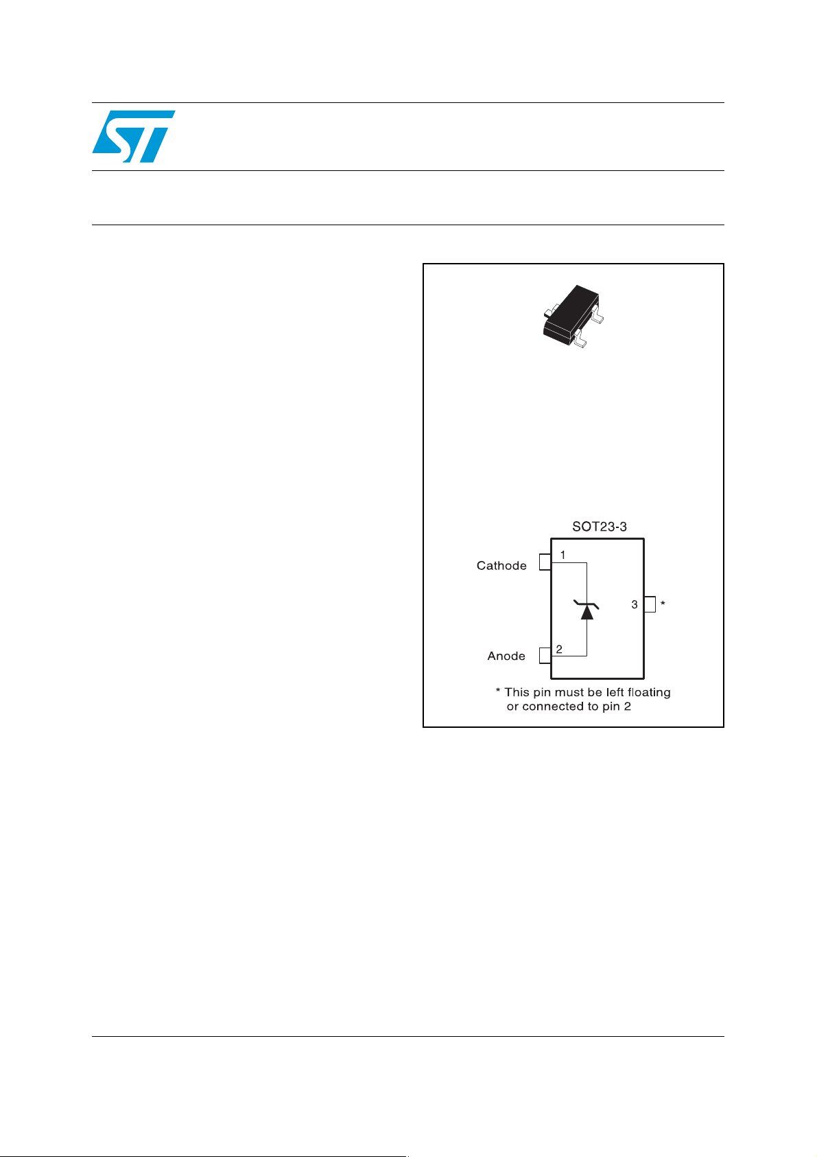
TS4041
L
SOT23-3L
(Plastic micropackage)
Pin connections
(Top view)
Description
The TS4041 is a low power shunt voltage
reference providing a stable 1.225V output
voltage over the industrial temperature range
(-40°C to +85°C). Availabe in SOT23-3 surface
mount package, it can be design ed in applications
where space saving is critical.
The low operating current is a key adv antage for
power restricted designs. In addition, the TS4041
is very stable and can be used in a broad ran ge of
application conditions.
August 2007 Rev 2 1/9
www.st.com
9
Page 2
Absolute maximum ratings and operating conditions TS4041
1 Absolute maximum ratings and operating conditions
Table 1. Absolute maximum ratings (AMR)
Symbol Parameter Value Unit
I
I
P
T
stg
ESD
T
lead
1. Pd is calculated with T
2. Human body model: 100pF discharged through a 1.5kΩ resistor between two pins of the device, done for
all couples of pin combinations with other pins floating.
3. Machine model: a 200pF cap is charged to the specified voltage, then discharged directly between two pins
of the device with no external series resistor (internal resistor < 5Ω), done for all couples of pin
combinations with other pins floating.
Table 2. Operating conditions
Reverse breakdown current 20 mA
k
Forward cur rent 10 mA
f
Power dissipation
d
(1)
SOT23-3
360 mW
Storage temperature -65 to +150 °C
(3)
(2)
2kV
200 V
Human body model (HBM)
Machine model (MM)
Lead temperature (soldering, 10 seconds) 260 °C
= 25°C and Tj = 150°C and R
amb
= 340°C/W for the SOT23-3L package.
thja
Symbol Parameter Value Unit
I
I
T
min
max
oper
Minimum operating current 65 μA
Maximum operating current 12 mA
Operating free air temperature range -40 to +85 °C
2/9
Page 3
TS4041 Electrical characteristics
2 Electrical characteristics
Table 3. TS4041E (2% precision) T
amb
= 25°C
(1)
(unless otherwise specified)
Symbol Parameter Test cond iti on s Min. Typ. Max. Unit
Reverse breakdown voltage Ik = 100μA
V
k
Reverse breakdown voltage tolerance
I
k-min
ΔV
ΔVk/ΔI
R
Minimum operating current
/ΔT Average temperature coefficient Ik = 100μA 150 ppm/°C
ref
Reverse breakdown voltage change
k
with operating current range
Static impedance ΔIk = 45µA to 1mA 0.25 0.5 Ω
ka
K
Long term stability Ik = 100μA, t = 1000hrs 120 ppm
vh
En Wide band noise I
1. Limits are 100% production tested at 25°C. Behavior at the temperature range limits is guaranteed through correlation and
by design.
Table 4. TS4041D (1% precision) T
amb
= 100μA
I
k
-40°C < T
T
amb
-40°C < T
I
k-min
-40°C < T
1mA < I
-40°C < T
= 100μA, 10Hz < f < 10kHz 200 nV/√Hz
k
= 25°C
< +85°C
amb
= 25°C 40 65
< +85°C 70
amb
< Ik < 1mA
< +85°C
amb
< 12mA
k
< +85°C
amb
(1)
(unless otherwise specified)
1.2001.2251.25
0
-25
-36
+25
+36
0.3 2
2.5
2.5 8
10
mV
μA
mV
Symbol Parameter Test cond iti on s Min. Typ. Max. Unit
V
Reverse breakdown voltage Ik = 100μA
V
k
Reverse breakdown voltage tolerance
Minimum operating current
/ΔT Average temperature coefficient Ik = 100μA 150 ppm/°C
ref
Reverse breakdown voltage change
/ΔI
k
k
with operating current range
Static impedance ΔIk = 45μA to 1mA 0.25 0.5 Ω
ka
Long term stability Ik = 100μA, t = 1000hrs 120 ppm
K
vh
ΔV
ΔV
I
k-min
R
En Wide band noise I
1. Limits are 100% production tested at 25°C. Behavior at the temperature range limits is guaranteed through correlation and
by design.
Ik = 100μA
-40°C < T
T
= 25°C 40 65
amb
-40°C < T
I
< Ik < 1mA
k-min
-40°C < T
1mA < I
-40°C < T
= 100μA, 10Hz < f < 10kHz 200 nV/√Hz
k
< +85°C
amb
< +85°C 70
amb
< +85°C
amb
< 12mA
k
< +85°C
amb
1.2131.2251.23
7
-12
-25
+12
+25
0.3 2
2.5
2.5 8
10
mV
μA
mV
V
3/9
Page 4
Electrical characteristics TS4041
Table 5. TS4041C (0.5% precision)
(1)
T
= 25°C (unless otherwise specified)
amb
Symbol Parameter Test cond iti on s Min. Typ. Max. Unit
Reverse breakdown voltage Ik = 100μA
V
k
Reverse breakdown voltage tolerance
I
k-min
ΔV
ΔVk/ΔI
R
Minimum operating current
/ΔT Average temperature coefficient Ik = 100μA 120 ppm/°C
ref
Reverse breakdown voltage change
k
with operating current range
Static impedance ΔIk = 45μA to 1mA 0.25 0.5 Ω
ka
K
Long term stability Ik = 100μA, t = 1000hrs 120 ppm
vh
En Wide band noise I
1. Limits are 100% production tested at 25°C. Behavior at the temperature range limits is guaranteed through correlation and
by design.
= 100μA
I
k
-40°C < T
T
= 25°C 40 60
amb
-40°C < T
< Ik < 1mA
I
k-min
-40°C < T
1mA < I
-40°C < T
= 100μA, 10Hz < f < 10kHz 200 nV/√Hz
k
< +85°C
amb
< +85°C 65
amb
< +85°C
amb
< 12mA
k
< +85°C
amb
1.2191.2251.23
1
-6
-16
+6
+16
0.3 1.5
2
2.5 6
8
mV
μA
mV
V
4/9
Page 5
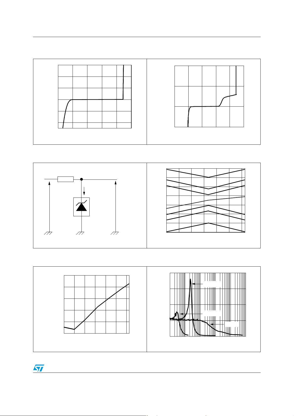
TS4041 Electrical characteristics
12
current
Figure 2. Reference voltage versus cathode
current
100
Figure 1. Reference voltage versus cathode
8
4
50
0
0
-4
Cathode current (mA)
Cathode current (µA)
-8
-50
-0.5
-1
-0.5
00.51
1.5
-1
Reference voltage (V)
0
0.5
Reference voltage (V)
1
Figure 3. Test circuit Figure 4. Reference voltage versus
temperature
1.26
R
Ik=(Vin-Vref)/R
Vout=Vref
1.25
1.24
1.23
1.22
1.5
+2%
+1%
+0.5%
Figure 5. Static impedance versus
temperature
0.25
0.24
0.23
0.22
0.21
Static impedance (Ohms)
0.2
-40 -20 0 20 40 60 80
Temperature (°C)
1.21
Cathode voltage (V)
1.2
1.19
-40 -20 0 20 40 60 80
Temperature (°C)
Figure 6. Noise voltage versus frequency
800
600
400
200
Noise voltage (nV/Hz)
0
0 1 10 100 1,000 10,000
CL=10µF
CL=100µF
CL=0µF
Frequency (kHz)
-0.5%
-1%
-2%
5/9
Page 6
Package information TS4041
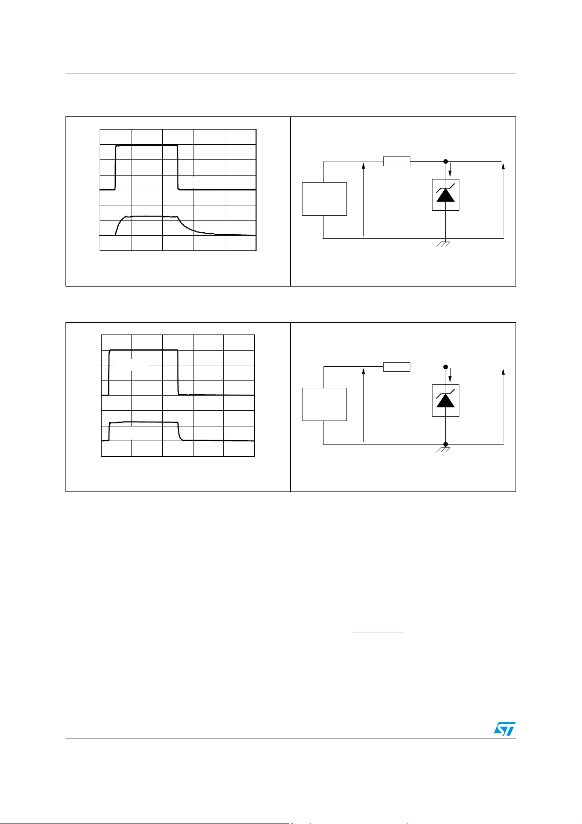
Figure 7. Pulse response for I
3V
0V
1.225V
0V
0246810
Time (µs)
=100µA Figure 8. Test circuit for pulse response at
k
Input
Output
Pulse
Generator
I
=100µA
k
Intput
18 K
Ω
Ik=100µA
Figure 9. Pulse response for Ik=1mA Figure 10. Test circuit for pulse response at
I
=1mA
k
3V
Input
Output
0V
Pulse
Generator
1.225V
0V
1.8 K
Ω
Intput
Ik=1mA
Output
Output
0246810
Time (µs)
3 Package information
In order to meet environmental requirements, STMicroelectronics offers these devices in
ECOPACK
category of second level interconnect is marke d on the pa ckage and on the inner box label,
in compliance with JEDEC Standard JESD97. The maximum ratings related t o soldering
conditions are also marked on the inner box label. ECOPACK is an STMicroelectronics
trademark. ECOPACK specifications are available at: www .st.com
6/9
®
packages. These packages have a lead-free second level interconnect. The
.
Page 7
TS4041 Package information
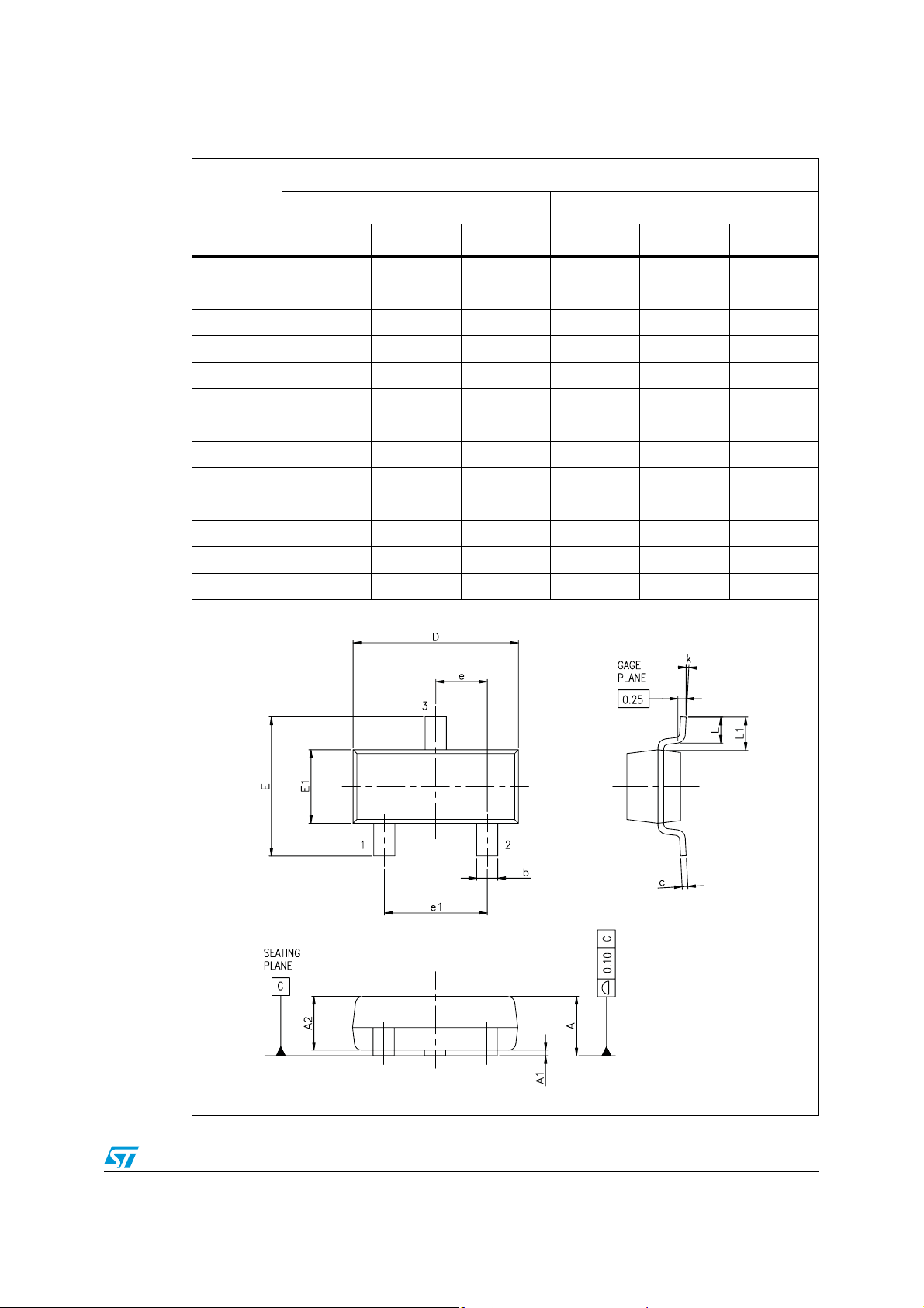
Figure 11. SOT23-3 package mechanical data
Dimensions
Ref.
Millimeters Mils
Min. Typ. Max. Min. Typ. Max.
A 0.890 1.120 35.05 44.12
A1 0.010 0.100 0.39 3.94
A2 0.880 0.950 1.020 34.65 37.41 40.17
b 0.300 0.500 11.81 19.69
C 0.080 0.200 3.15 7.88
D 2.800 2.900 3.040 110.26 114.17 119.72
E 2.100 2.64 82.70 103.96
E1 1.200 1.300 1.400 47.26 51.19 55.13
e 0.950 37.41
e1 1.900 74.82
L 0.400 0.600 15.75 23.63
L1 0.540 21.27
k0°8°0°8°
7110469/A
7/9
Page 8
Ordering information TS4041
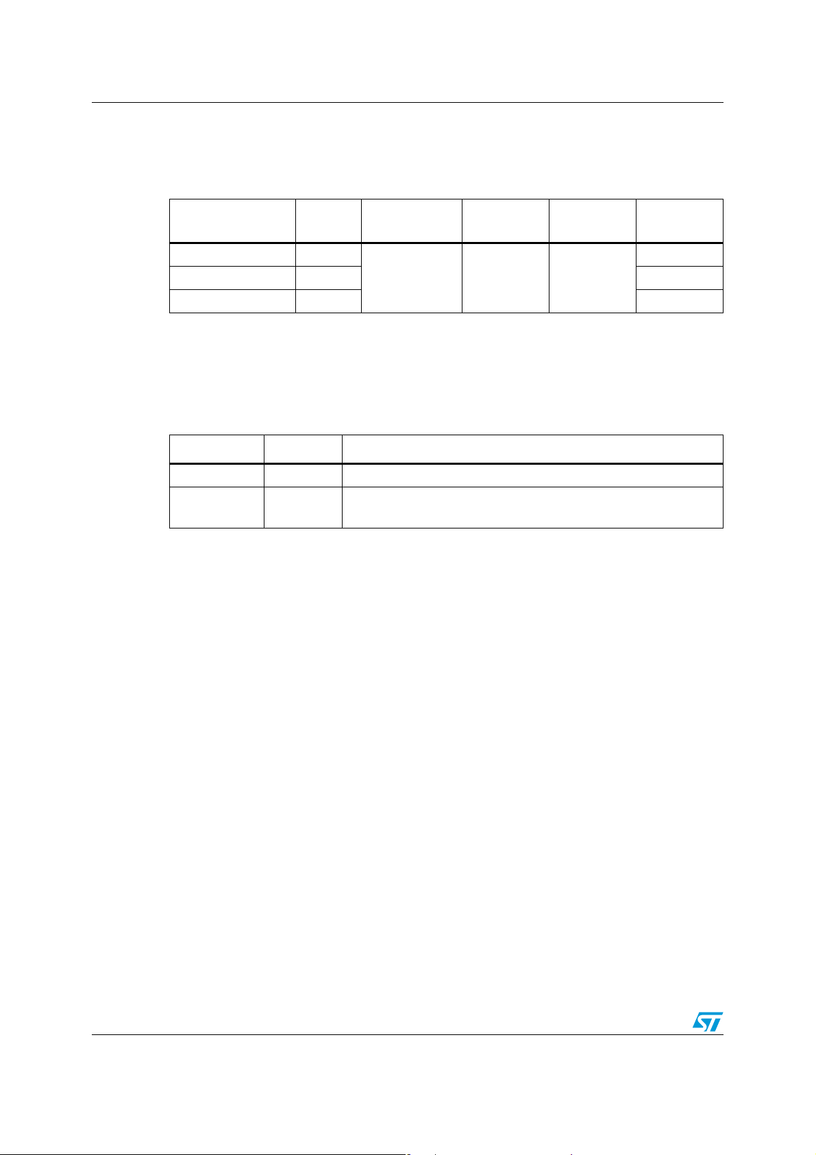
4 Ordering information
Table 6. Order codes
Part number Precision
TS4041EILT-1.2 2%
TS4041DILT-1.2 1% L232
TS4041CILT-1.2 0.5% L231
5 Revision history
Table 7. Document revision history
Date Revision Changes
21-Mar-2002 1 Initial release.
20-Aug-2007 2
Temperature
range
-40°C to +85°C SOT23-3 Tape & reel
Removed TO-92 package information.
Format update.
Package Packing Marking
L233
8/9
Page 9

TS4041
Please Read Carefully:
Information in this document is provided solely in connection with ST products. STMicroelectronics NV and its subsidiaries (“ST”) reserve the
right to make changes, corrections, modifications or improvements, to this document, and the products and services described herein at any
time, without notice.
All ST products are sold pursuant to ST’s terms and conditions of sale.
Purchasers are solely res ponsibl e fo r the c hoic e, se lecti on an d use o f the S T prod ucts and s ervi ces d escr ibed he rein , and ST as sumes no
liability whatsoever relati ng to the choice, selection or use o f the ST products and services described herein.
No license, express or implied, by estoppel or otherwise, to any intellectual property rights is granted under this document. If any part of this
document refers to any third pa rty p ro duc ts or se rv ices it sh all n ot be deem ed a lice ns e gr ant by ST fo r t he use of su ch thi r d party products
or services, or any intellectua l property c ontained the rein or consi dered as a warr anty coverin g the use in any manner whats oever of suc h
third party products or servi ces or any intellectual property contained therein.
UNLESS OTHERWISE SET FORTH IN ST’S TERMS AND CONDITIONS OF SALE ST DISCLAIMS ANY EXPRESS OR IMPLIED
WARRANTY WITH RESPECT TO THE USE AND/OR SALE OF ST PRODUCTS INCLUDING WITHOUT LIMITATION IMPLIED
WARRANTIES OF MERCHANTABILITY, FITNESS FOR A PARTICUL AR PURPOS E (AND THEIR EQUIVALE NTS UNDER THE LAWS
OF ANY JURISDICTION), OR INFRINGEMENT OF ANY PATENT, COPYRIGHT OR OTHER INTELLECTUAL PROPERTY RIGHT.
UNLESS EXPRESSLY APPROVED IN WRITING BY AN AUTHORIZED ST REPRESENTATIVE, ST PRODUCTS ARE NOT
RECOMMENDED, AUTHORIZED OR WARRANTED FOR USE IN MILITARY, AIR CRAFT, SPACE, LIFE SAVING, OR LIFE SUSTAINING
APPLICATIONS, NOR IN PRODUCTS OR SYSTEMS WHERE FAILURE OR MALFUNCTION MAY RESULT IN PERSONAL INJ URY,
DEATH, OR SEVERE PROPERTY OR ENVIRONMENTAL DAMAGE. ST PRODUCTS WHICH ARE NOT SPECIFIED AS "AUTOMOTIVE
GRADE" MAY ONLY BE USED IN AUTOMOTIVE APPLICATIONS AT USER’S OWN RISK.
Resale of ST products with provisions different from the statements and/or technical features set forth in this document shall immediately void
any warranty granted by ST fo r the ST pro duct or serv ice describe d herein and shall not cr eate or exten d in any manne r whatsoever , any
liability of ST.
ST and the ST logo are trademarks or registered trademarks of ST in various countries.
Information in this document su persedes and replaces all information previously supplied.
The ST logo is a registered trademark of STMicroelectronics. All other names are the property of their respective owners.
© 2007 STMicroelectronics - All rights reserved
STMicroelectronics group of compan ie s
Australia - Belgium - Brazil - Canada - China - Czech Republic - Finland - France - Germany - Hong Kong - India - Israel - I taly - Japan -
Malaysia - Malta - Morocco - Singapore - Spain - Sweden - Switzerland - United Kingdom - United States of America
www.st.com
9/9
 Loading...