

Page 1
Programmable shunt voltage reference
Features
■ Adjustable output voltage: 2.5 to 24 V
■ Precision selection at 25 °C: ± 2%, ± 1% and
±0.5%
■ Sink current capability: 1 to 100 mA
■ Industrial temperature range: - 40 to +105 °C
■ Performances compatible with industry-
standard TL431
TS2431
Datasheet − production data
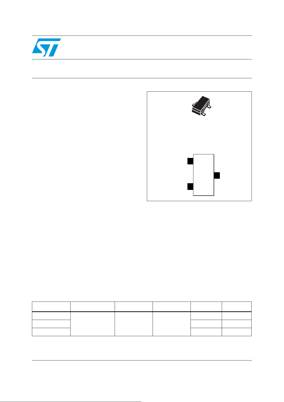
SOT23-3L
(plastic micropackage)
Pin connections (top view)
Applications
■ Computers
■ Instrumentation
■ Battery chargers
■ Switch mode power supplies
■ Battery-operated equipment
Description
The TS2431 is a programmable shunt voltage
reference with guaranteed temperature stability
over the entire temperature range of operation
- 40 to + 105 °C. The output voltage may be set to
any value between 2.5 and 24 V with an external
resistor bridge. Available in a SOT23-3L surface
mount package, the device can be implemented
in applications where space-saving is of utmost
importance.
Cathode
Reference
1
Anode
3
TS2431
2
Table 1. Device summary
Order codes Temperature range Package Packing Precision Marking
TS2431ILT
TS2431AILT 1% L286
TS2431BILT 0.5% L287
May 2012 Doc ID 7961 Rev 3 1/11
This is information on a product in full production.
-40 to +105°C SOT23-3L Tape and reel
2% L285
www.st.com
11
Page 2

Contents TS2431
Contents
1 Absolute maximum ratings and operating conditions . . . . . . . . . . . . . 3
2 Electrical characteristics . . . . . . . . . . . . . . . . . . . . . . . . . . . . . . . . . . . . . 4
3 Package information . . . . . . . . . . . . . . . . . . . . . . . . . . . . . . . . . . . . . . . . . 8
3.1 SOT23-3L package information . . . . . . . . . . . . . . . . . . . . . . . . . . . . . . . . . 9
4 Revision history . . . . . . . . . . . . . . . . . . . . . . . . . . . . . . . . . . . . . . . . . . . 10
2/11 Doc ID 7961 Rev 3
Page 3
TS2431 Absolute maximum ratings and operating conditions
1 Absolute maximum ratings and operating conditions
Table 2. Absolute maximum ratings
Symbol Parameter Value Unit
Vka Cathode to anode voltage 25 V
I
K
I
REF
P
T
std
ESD
T
LEAD
1. Pd has been calculated with Tamb = 25°C, Tjunction = 150°C, Rthjc = 110°C/W and Rthja = 340°C/W for
the SOT23-3 package.
2. Human body model: a 100 pF capacitor is charged to the specified voltage, then discharged through a
1.5 kΩ resistor between two pins of the device. This is done for all couples of connected pin combinations
while the other pins are floating.
3. Machine model: a 200 pF capacitor is charged to the specified voltage, then discharged directly between
two pins of the device with no external series resistor (internal resistor < 5 Ω). This is done for all couples of
connected pin combinations while the other pins are floating.
Table 3. Operating conditions
Reverse breakdown current -100 to +150 mA
Reference input current range -0.05 to +10 mA
Power dissipation
d
(1)
SOT23-3L
360 mW
Storage temperature -65 to +150 °C
(3)
(2)
2kV
200 V
Human body model (HBM)
Machine model (MM)
Lead temperature (soldering, 10 seconds) 260 °C
Symbol Parameter Value Unit
V
KA
I
K
T
oper
1. Maximum power dissipation must be strictly observed to avoid damaging the component.
Cathode to anode voltage V
Cathode operating current
(1)
to 24 V
REF
1 to 100 mA
Operating free air temperature range - 40 to + 105 °C
Doc ID 7961 Rev 3 3/11
Page 4

Electrical characteristics TS2431
2 Electrical characteristics
Table 4. Electrical characteristics (Tamb = 25 °C unless otherwise specified)
Symbol Parameter Test condition Min. Typ. Max. Unit
V
= V
K
, IK = 10 mA 2.5
REF
TS2431 (2%) 2.45 2.55
V
Reference input voltage
REF
TS2431A (1%) 2.475 2.525
TS2431B (0.5%) 2.488 2.512
0 °C < T < +70 °C 10 20
-40 °C < T < +105 °C 20 35
-40 °C < T < +105 °C 50 100 ppm/°C
|ΔV
Reference input voltage deviation over
|
temperature
T
REF
C
= V
V
K
, IK = 10 mA
REF
Temperature coefficient
(1) (2)
(2)
T = 25 °C 0.3 0.8
I
KMIN
ΔVref
------------ --- -
ΔVk
I
|ΔI
I
|Z
Minimum operating current
Ratio of change in reference input
voltage to change in cathode to anode
voltage
Reference input current
REF
REF
OFF
KA
= 10 mA, R1 = 10 kΩ, R2 = +
I
K
Reference input current deviation
|
= 10 mA, R1 = 10 kΩ, R2 = +
I
K
Off-state cathode current VK = 24 V, V
| Reverse dynamic impedance
(3)
∞
(3)
∞
-40 °C < T < +105 °C 1
= 10 mA
I
K
Vka = 24 to 2.5 V
0.3 2 mV/V
T = 25 °C 0.5 2.5
-40 °C < T < +105 °C 3
-40 °C < T < +105 °C 0.4 1.2 µA
= GND 10 500 nA
REF
V
= V
K
REF
ΔIK = 1 to 50 mA,
0.5 0.75 W
f < 10 kHz
= 10 mA
I
E
N
Wide band noise
K
10 Hz < f < 10 kHz
300 nV/√Hz
V
mV-40 °C < T < +85 °C 17 30
mA
µA
1. Limits are 100% production tested at 25° C. Limits over temperature are guaranteed through correlation and by design.
|ΔV
2.
3. Refer to
| is defined as the difference between the maximum and minimum values of V
REF
range.
Figure 4: Test circuit for Vka = Vref on page 5
.
obtained over the full temperature
REF
4/11 Doc ID 7961 Rev 3
Page 5

TS2431 Electrical characteristics
Figure 1. Reference voltage vs. temperature Figure 2. Cathode voltage vs. cathode
current
2.52
2.51
2.50
Voltage reference (V)
2.49
2.48
-40-200 20406080100
Temperatur e (°C)
Ik =10 mA
Vka = Vref
Figure 3. Reference input current vs.
Figure 4. Test circuit for Vka = Vref
3
2
1
0
Vka Cathod e voltage (V)
-1
-0.10 -0.05 0.00 0.05 0.10
Ika Cathode current (A)
Vka = Vref
T=25°C
temperature
1.00
0.75
Ik=10mA
R1=10K
R2=+∞
Ω
Input
Ik
Output
0.50
Reference input current (µA)
0.25
0.00
-40-200 20406080100
Temperatur e (°C)
Figure 5. Cathode voltage vs. cathode
current
3
T=-40°C
2
1
Vka Cathode voltage (V)
T=+105°C
0
0 100 200 300 400
T=+25°C
Vka = Vref
Ik Cathode current (µA)
Vka
Vref
Figure 6. Dynamic impedance vs. frequency
5
4
3
2
Zka Dynamic impedance (Ohms )
1
0
10 100 1000 10000 100000 1000000
Vka=Vref
Ik=1mA
T=25°C
Frequency (Hz)
Doc ID 7961 Rev 3 5/11
Page 6

Electrical characteristics TS2431
Figure 7. Off-state current vs. temperature Figure 8. Ratio of change in reference input
voltage to change in Vka voltage vs.
temperature
0.3
0.2
Off-state current (µA)
0.1
0.0
-40-20 0 20406080100
Temperatur e (°C)
0.4
0.3
0.2
ΔVref / ΔVka (mV/V)
0.1
0.0
-40-20 0 20406080100
Temperatur e (°C)
ΔVka=24 to 2.5V
Ik=10mA
T=25°C
Figure 9. Phase and gain vs. frequency Figure 10. Test circuit for off-state current
measurement
Vka=24V
Ioff
Figure 11. Test circuit for Vka > Vref Figure 12. Test circuit for phase and gain
measurement
Input
R1
R2
Iref
Vref
Vka = Vref . (1+R1/R2) + Iref . R1
Ik
Vka
6/11 Doc ID 7961 Rev 3
Page 7

TS2431 Electrical characteristics
Figure 13. Pulse response at Ik = 0 to 1 mA Figure 14. Pulse response at Ik = 1 to 0 mA
6
4
Voltage (V)
2
0
0.0 0.5 1.0 1.5 2.0
Input voltage
Output vol tage
Time (µs)
Ik= 0 to 1mA
T=25°C
6
Input voltage
4
Ik= 1mA to 0
T=25°C
Voltage (V)
2
0
0.00.51.01.52.0
Output voltage
Time (µs)
Figure 15. Stability boundary conditions Figure 16. Test circuit for pulse response at
Ik = 1 mA
100
80
60
Vka=3 V
40
Cathode curr ent (mA)
20
Vka=2.5 V
0
1E-10 1E-9 1E-8 1E-7 1E-6 1E-5
Instable
area
Capacitive load (F)
Stable
area
Vka=5 V
Pulse
Generator
F=100kHz
0 to 5V
Intput
2.5 K
Ω
Ik=1mA
Output
Figure 17. Equivalent input noise vs.
frequency
300
250
200
150
100
Noise (nV / √ Hz)
50
0
0.1 1 10 100 1000
Vka=Vref
Ik=1mA
T=25°C
Frequency (KHz)
Figure 18. Block diagram
Doc ID 7961 Rev 3 7/11
Page 8

Package mechanical data TS2431
3 Package mechanical data
In order to meet environmental requirements, ST offers these devices in different grades of
ECOPACK
specifications, grade definitions and product status are available at:
ECOPACK
®
packages, depending on their level of environmental compliance. ECOPACK®
®
is an ST trademark.
www.st.com
.
8/11 Doc ID 7961 Rev 3
Page 9

TS2431 Package mechanical data
3.1 SOT23-3L package information
Figure 19. SOT23-3L package mechanical drawing
Table 5. SOT23-3L package mechanical data
Dimensions
Millimeters Inches
Ref.
Min. Typ. Max. Min. Typ. Max.
A 0.89 1.12 0.035 0.044
A1 0.01 0.10 0.0004 0.004
A2 0.88 0.95 1.02 0.035 0.037 0.040
b 0.30 0.50 0.012 0.020
c 0.08 0.20 0.003 0.008
D 2.80 2.90 3.04 0.110 0.114 0.120
E 2.10 2.64 0.083 0.104
E1 1.20 1.30 1.40 0.047 0.051 0.055
e 0.95 0.037
e1 1.90 0.075
L 0.40 0.50 0.60 0.016 0.020 0.024
L1 0.54 0.021
k0d 8d
Doc ID 7961 Rev 3 9/11
Page 10

Revision history TS2431
4 Revision history
Table 6. Document revision history
Date Revision Changes
01-Feb-2002 1 Initial release.
Updated document format.
10-Sep-2009 2
Modified footnote 1 under
on page 3
Added HBM and MM notes under
.
Table 2: Absolute maximum ratings
Ta bl e 2
.
11-May-2012 3 Removed: automotive grade order codes
Table 1 on page 1
.
10/11 Doc ID 7961 Rev 3
Page 11

TS2431
Please Read Carefully:
Information in this document is provided solely in connection with ST products. STMicroelectronics NV and its subsidiaries (“ST”) reserve the
right to make changes, corrections, modifications or improvements, to this document, and the products and services described herein at any
time, without notice.
All ST products are sold pursuant to ST’s terms and conditions of sale.
Purchasers are solely responsible for the choice, selection and use of the ST products and services described herein, and ST assumes no
liability whatsoever relating to the choice, selection or use of the ST products and services described herein.
No license, express or implied, by estoppel or otherwise, to any intellectual property rights is granted under this document. If any part of this
document refers to any third party products or services it shall not be deemed a license grant by ST for the use of such third party products
or services, or any intellectual property contained therein or considered as a warranty covering the use in any manner whatsoever of such
third party products or services or any intellectual property contained therein.
UNLESS OTHERWISE SET FORTH IN ST’S TERMS AND CONDITIONS OF SALE ST DISCLAIMS ANY EXPRESS OR IMPLIED
WARRANTY WITH RESPECT TO THE USE AND/OR SALE OF ST PRODUCTS INCLUDING WITHOUT LIMITATION IMPLIED
WARRANTIES OF MERCHANTABILITY, FITNESS FOR A PARTICULAR PURPOSE (AND THEIR EQUIVALENTS UNDER THE LAWS
OF ANY JURISDICTION), OR INFRINGEMENT OF ANY PATENT, COPYRIGHT OR OTHER INTELLECTUAL PROPERTY RIGHT.
UNLESS EXPRESSLY APPROVED IN WRITING BY TWO AUTHORIZED ST REPRESENTATIVES, ST PRODUCTS ARE NOT
RECOMMENDED, AUTHORIZED OR WARRANTED FOR USE IN MILITARY, AIR CRAFT, SPACE, LIFE SAVING, OR LIFE SUSTAINING
APPLICATIONS, NOR IN PRODUCTS OR SYSTEMS WHERE FAILURE OR MALFUNCTION MAY RESULT IN PERSONAL INJURY,
DEATH, OR SEVERE PROPERTY OR ENVIRONMENTAL DAMAGE. ST PRODUCTS WHICH ARE NOT SPECIFIED AS "AUTOMOTIVE
GRADE" MAY ONLY BE USED IN AUTOMOTIVE APPLICATIONS AT USER’S OWN RISK.
Resale of ST products with provisions different from the statements and/or technical features set forth in this document shall immediately void
any warranty granted by ST for the ST product or service described herein and shall not create or extend in any manner whatsoever, any
liability of ST.
ST and the ST logo are trademarks or registered trademarks of ST in various countries.
Information in this document supersedes and replaces all information previously supplied.
The ST logo is a registered trademark of STMicroelectronics. All other names are the property of their respective owners.
© 2012 STMicroelectronics - All rights reserved
STMicroelectronics group of companies
Australia - Belgium - Brazil - Canada - China - Czech Republic - Finland - France - Germany - Hong Kong - India - Israel - Italy - Japan -
Malaysia - Malta - Morocco - Philippines - Singapore - Spain - Sweden - Switzerland - United Kingdom - United States of America
www.st.com
Doc ID 7961 Rev 3 11/11
 Loading...