

Page 1
TS19705
Single-Stage PFC
Primary-Side-Regulation LED Driver
1/7 Version: A14
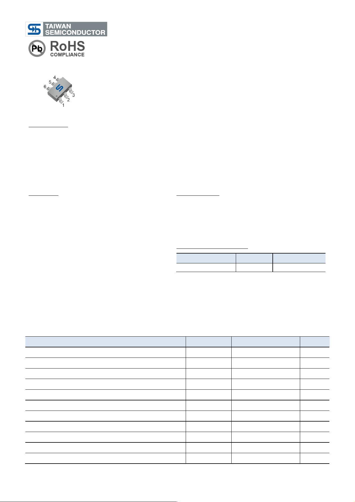
SOT-26
Description
TS19705 is a primary-side-regulation with Fly-back control IC with active power factor correction function for LED
lighting applications. The IC achieves high power factor and low Total Harmonic Distortion (THD) operation by
Boundary Conduction Mode (BCM). The line and load regulation of LED current is about <±3% because of
particular control method.
TS19705 also provides gate driving voltage clamping, VCC overvoltage protection and system output open/short
circuit protection to increase IC performance.
Features
● Accuracy Constant Current <±3%
● Low BOM Cost
● Primary-side feedback control
● Application Voltage Range: 90~ 264VAC
● Transition-mode PFC operating
● Built-in Active Power Factor Correction
● Constant Output Current Control
● Good Line and Load Regulation
● Open-LED Protection on DMG pin
● Over-Voltage Protection on VCC pin
● Short-LED Protection
● Cycle by Cycle Over Current Protection on CS pin
● Over-Temperature Protection
● Gate Driving Voltage Clamping
Applications
● E27, T5, T8 LED lighting
● Bulb
● Down Light
● LED Lighting Applications
Ordering Information
Part No.
Package
Packing
TS19705CX6 RFG
SOT-26
3kpcs / 7” Reel
Note: “G” denote for Halogen Free Product
Absolute Maximum Ratings (T
A
= 25oC unless otherwise noted)
Parameter
Symbol
Range
Unit
Power supply pin
VCC
40
V
DMG voltage to GND
V
DMG
-0.3 to 40
V
OUT voltage to GND
V
OUT
-0.3 to 40
V
CS voltage to GND
VCS
-0.3 to 5.5
V
COM voltage to GND
V
COM
-0.3 to 5
V
Junction Temperature Range
TJ
-40 to +150
°C
Storage Temperature Range
T
STG
-65 to +150
°C
Power Dissipation @TA=25 °C
PD
0.3
W
Thermal Resistance Junction to Ambient (Note 2)
RθJA
220
°C/W
Thermal Resistance Junction to Case
RθJC
106.6
°C/W
ESD Rating (Human Body Model)
ESD
2
kV
Pin Definition:
1. Compensation
2. Ground
3. Current Sense
4. Output
5. VCC
6. DMG
Page 2
TS19705
Single-Stage PFC
Primary-Side-Regulation LED Driver
2/7 Version: A14
Recommended Operating Conditions
Parameter
Symbol
Conditions
Unit
Power supply pin
VCC
38
V
DMG voltage to GND
V
DMG
-0.3 to 38
V
OUT voltage to GND
V
OUT
-0.3 to 38
V
CS voltage to GND
VCS
-0.3 to 5
V
COM voltage to GND
V
COM
-0.3 to VCC
V
Operating Junction Temperature Range
TJ
-40 to +125
°C
Operating Ambient Temperature Range
T
OPA
-40 to +85
°C
Electrical Characteristics (V
CC
=15 , TA=25℃, unless otherwise specified)
Parameter
Symbol
Condition
Min
Typ
Max
Unit
Turn-on voltage
V
CC_ON
17
18
19
V
Turn-off voltage
V
CC_OFF
8.5
9.5
10
V
Quiescent current 1
IQ1
VCC=17V, @ VCC off
--
30
50
µA
Quiescent current 2
IQ2
Start-up @ 4.5kHz
--
600
800
µA
Operation supply current
ICC
--
2.5
3..0
mA
Protection
VCC voltage protection
V
OVPA
31
32
34
V
Output voltage protection
V
OVPS
10
10.5
11
V
CS limit voltage
V
OCP
1.15
1.25
1.35
V
Short circuit protection
V
SCP
Guaranteed by design
-- 3 -- V Oscillator
Start-up timer
t
STR
--
220
--
µs
GM Amplifier
Transconductance
gm
--
60
--
µA/V
Source current
I
COMP_SOU
--
20
--
µA
Driver
Dropout voltage
VOH
VCC=33V, IO = 10mA
--
1.2
1.5
V
VOL
VCC=33V, IO = -10mA
--
0.12
-- V Rising time
tr
VCC=20V, CO =1nF
--
40
--
ns
Falling time
tf
VCC=20V, CO =1nF
--
80
--
ns
Output clamp voltage
V
O_CLAMP
--
--
19
V
Leading edge blanking time
LEBt
--
0.5
--
ns
Note:
1. Stresses beyond those listed under “Absolute Maximum Ratings” may cause permanent damage to the device.
2. Thermal Resistance is specified with the component mounted on a low effective thermal conductivity test board
in free air at TA=25°C.
Page 3
TS19705
Single-Stage PFC
Primary-Side-Regulation LED Driver
3/7 Version: A14
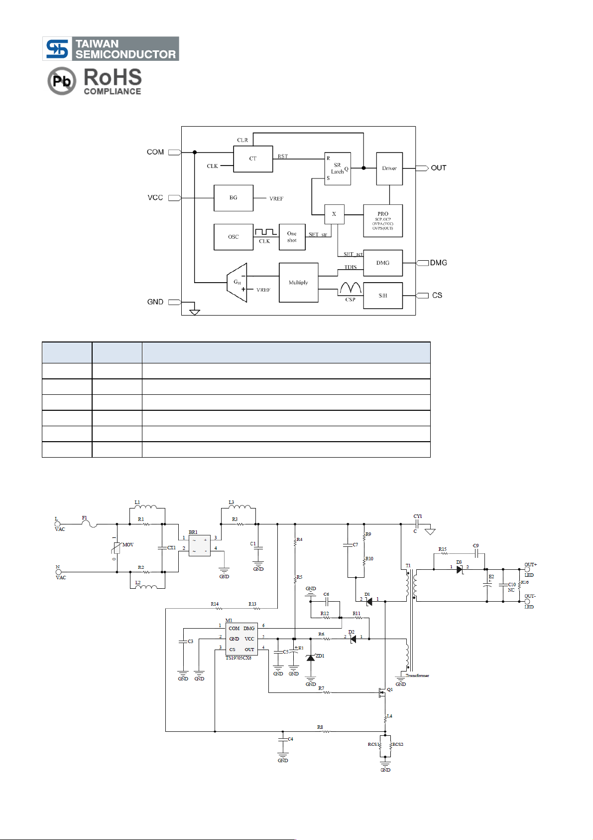
Function Block
Pin Description
Pin No.
Name
Function
1
COM
Output pin of error amplifier.
2
GND
Ground return for all internal circuitry.
3
CS
Input current sense pin.
4
OUT
Power MOS output pin.
5
VCC
Power supply pin for all internal circuitry.
6
DMG
Zero current demagnetization sensing.
Typical Application Circuit
Page 4

TS19705
Single-Stage PFC
Primary-Side-Regulation LED Driver
4/7 Version: A14
Application Information
Function Description
The TS19705 is a constant current Fly-back controller with primary side control and PFC function for LED lighting
applications. The controller is Boundary Conduction Mode (BCM) operation with constant on time based regulator
design to achieve high power factor performance.
The TS19705 has built-in VCC over voltage protection, open LED protection, short LED protection, over temperature
protection, primary side current limit and gate clamp functions.
The average output current can be expressed as below.
Where :
! I
O_avg
is the average output current
! NP is the primary-side turn ratio
! NS is the secondary-side turn ratio
! RS is the sensing resistor connected between the MOSFET source and the GND
Pin Detail
Compensation
This is the output of the gm amplifier. Connect with a suitable RC network to ground.
Ground
GND is the reference node of internal circuit.
Current Sense
MOSFET current signal sensing for multiplication and current limit setting function.
Where :
! ICS is the input current sence
! RS is the sensing resistor connected between the MOSFET source and GND
Output
Gate drive for external MOSFET switch and is built-in gate clamp function.
VCC
Power supply for the controller during normal operation. The controller will start up when VCC reaches 18V (typical)
and will shut-down when VCC voltage is below 9.5V (typical). A decoupling capacitor should be connected between
the VCC and GND pin as close as possible.
The TS19705 performs VCC over voltage protection though VCC pin. Once VCC pin exceeds in 32V, TS19705 turns
off and latchs out the MOSFET switcher until VCC goes below V
CC_OFF
.
Page 5

TS19705
Single-Stage PFC
Primary-Side-Regulation LED Driver
5/7 Version: A14
Application Information (Continue)
DMG
The Output voltage is reflected by the auxiliary winding (N
AUX
) voltage of Flyback transformer, the DMG pin can
sense output information to depart from start up voltage (V
O_STR
) and protection voltage (V
O_OVP
).
When DMG sense voltage under V
O_STR
, the circuit will work on short circuit protection, f
STR
=1/t
STR
.
When DMG sense voltage over V
O_OVP
, the circuit will work on over voltage protection, it will latchs out until VCC
goes below V
CC_OFF
.
Where :
! V
OUT_OVP
is the output-over-voltage protection point
! V
OVPS
is the over voltage protection signal
! V
O_STR
is the start-up timer
! N
AUX
is the number of auxiliary-winding turns
! N
SEC
is the number of secondary-winding turns
Page 6

TS19705
Single-Stage PFC
Primary-Side-Regulation LED Driver
6/7 Version: A14
SOT-26 Mechanical Drawing
Unit: Millimeters
Marking Diagram
RG
= Device Code
L
= Lot Code A~Z
Y
= Year Code
(D=2014, E=2015, F=2016, G=2017, H=2018, J=2019, K=2020)
W
= Week Code
A~Z = wk1~wk26
A~Z = wk27~wk52
Page 7

TS19705
Single-Stage PFC
Primary-Side-Regulation LED Driver
7/7 Version: A14
Notice
Specifications of the products displayed herein are subject to change without notice. TSC or anyone on its behalf,
assumes no responsibility or liability for any errors or inaccuracies.
Information contained herein is intended to provide a product description only. No license, express or implied, to
any intellectual property rights is granted by this document. Except as provided in TSC’s terms and conditions of
sale for such products, TSC assumes no liability whatsoever, and disclaims any express or implied warranty,
relating to sale and/or use of TSC products including liability or warranties relating to fitness for a particular purpose,
merchantability, or infringement of any patent, copyright, or other intellectual property right.
The products shown herein are not designed for use in medical, life-saving, or life-sustaining applications.
Customers using or selling these products for use in such applications do so at their own risk and agree to fully
indemnify TSC for any damages resulting from such improper use or sale.
Page 8

 Loading...