

Page 1
TS19702
High Power Factor Corrector LED Driver
1/9 Version: A12
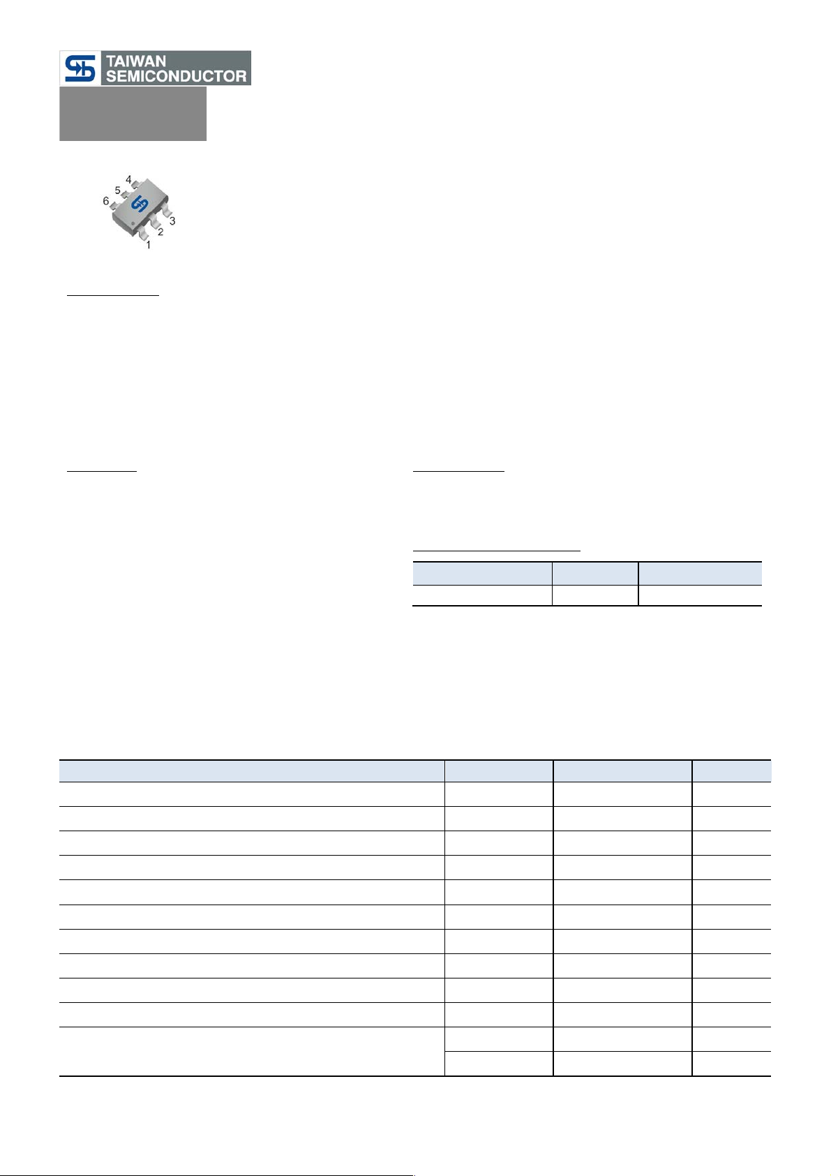
SOT-26
Description
The TS19702 is a h ig hly-integrated, lo w startup curr e n t , average current mode, one cycle control PFC and fixed
switching frequency PWM controller. These fun c tio n s enable the LED driver to easily meet the accuracy
average LE D current and high power factor requirements. The integrated functions also include the LED short
protection, open protection, and internal over temperature protection. The COMP pin controls the duty by
connected an RC compensation network to ground and formi ng the closed loop feedback control. To protect the
external power MOSFET from being damaged by supply over voltage, the TS19702 Output pin voltage is
clamped to about 15V.
Features
● High Power Factor by One Cycle Control
● Accuracy Constant Current
● Low BOM Cost
● Linear Dimming on DIM Pin
● Average Current / Fixed Frequency Control
● Gate Output Voltage Clamp
● LED Open Protection (OVP)
● LED Short Protection (SCP)
● Over Current Protection (OCP)
● Internal OTP Protection
● 300mA Driving Capability for Output Pin
● Application voltage range: 80V
AC
~ 308VAC
Application
● E27, T5, T8 LED lighting
● LED Lighting Applications
Ordering Information
Part No.
Package
Packing
TS19702CX6 RFG
SOT-26
3kpcs / 7” Reel
Note: “G” denote for Halogen Free Product
Absolute Maximum Ratings (Ta = 25
o
C unless otherwise noted)
Parameter
Symbol
Limit
Unit
Supply Voltage
VCC
30
V
Compensation Voltage
V
COMP
-0.3 ~ 7
V
Dimming Pin
V
DIM
-0.3 ~ 7
V
Current Sense Pin
V
CS
-0.3 ~ 7
V
Output Pin
V
OUT
15
V
Power Dissipation @ TA=85ºC
PD
250
mW
Operating Ambient Temperature
T
OPR
-20 ~ +85
o
C
Junction Temperature
TJ
+150
o
C
Storage Temperature Range
T
STG
-65 ~ +150
o
C
Thermal Resistance - Junction to Ambient
RӨJA
250
o
C/W
ESD Voltage Protection
HBM
2
KV
MM
200
V
Pin Definition:
1. VCC
2. Ground
3. Output
4. Dimming
5. Compensation
6. Current Sense
Page 2
TS19702
High Power Factor Corrector LED Driver
2/9 Version: A12
Electrical Characteristics (V
CC
=15 , TA=25℃, unless otherw is e s p ecified.)
Parameter
Symbol
Min.
Typ.
Max.
Unit
Supply Voltage
Startup Current (VCC=UVLO on - 1V)
I
START
-- 8 15
µA
Operating Current (with 1nF load on OUT pin),
Vcomp = 2.5V
I
OPR
-- 2 3
mA
Operating Current (with 1nF load on OUT pin),
Protection Tripped (OCP, OVP, SCP, OTP)
I
OPR
--
0.7 1 mA
UVLO(off)
UVLO
OFF
7 8 9
V
UVLO(on)
UVLOON
14
15
16
V
OVP Level on VCC Pin
V
OVP
26.5
28
29.5
V
OVP De-Bounce Time
T
OVP
--
40
--
µs
Voltage Feedback
Feedback Reference Voltage
VFB
0.196
0.200
0.204
V
Tran-Conductance
--
120
--
µs
Output Sink Current
I
SINK
--
12
--
µA
Output Source Current
I
SOURCE
--
12
--
µA
Current Sensing
Input Over Voltage Protection
V
IN-PROTECT
0.7
0.80
0.9
V
Open Loop Voltage, CS Pin Open
VCS
-- 5 --
V
Leading-Edge Blanking Time
TLE
--
410
--
ns
Delay to Output
T
O-DELAY
--
100
220
ns
Switching Frequency
Switching Frequency
FSW
42
45
48
KHz
Maximum Duty
D
(MAX)
90
--
--
%
Frequency Jitter Range
--
+/-4
--
%
Temp. Stability (-40°C ~ 125°C)
TEMP
STB
--
--
6
%
Voltage Stability (VCC = 11V~25V)
V
STB
--
--
1
%
GATE DRIVER OUTPUT
Rising Time, Load Capacitance =1000pF
T
RISING
--
160
320
ns
Falling Time, Load Capacitance =1000pF
T
FALLING
--
80
160
ns
VGATE-Clamp (VCC= 25V)
V
GATE
--
13.5
15
V
DIM INPUT SECTION
Saturation Threshold Voltage
SATTH
3.0
--
--
V
Linear Dimming Range
DIM
0.3
--
3.0
V
LED Current off Threshold Voltage
IOFFTH
--
--
0.3
V
Current Source
CS
290
300
310
µA
OTP SECTION
OTP Trip Point
OTPTP
140
150
160 oC
OTP Release Point
OTPRP
120
130
140 oC
OTP Threshold Level
OTPTH
--
20
-- oC
OTP De-Bounce Time
OTP
DBT
40
80
120
µs
Note 1: OCP, SCP, OTP: Auto Recovery Type
Note 2: OVP, Auto Recovery Type (Latch off type optional)
Page 3
TS19702
High Power Factor Corrector LED Driver
3/9 Version: A12
Function Block
Pin Description
Pin No.
Name
Function
1
VCC
Power supply pin
2
GND
Ground pin
3
OUT
The output driver for driving the external MOSFET
4
DIM
Dimming control pin by input a DC voltage
5
COMP
Feedback compensation network
6
CS
Current sense pin, connect to sense the MOSFET current
Page 4

TS19702
High Power Factor Corrector LED Driver
4/9 Version: A12
Application Circuit
Application Information
Start-up Current
The typical start-up current is around 8µA. Very low start-up current allows the PWM controller to increase the
value of start-up resistor and then reduce the power dissipation on it.
UVLO (Under Voltage Lockout)
A hysteresis UVLO comparator is implemented in TS19702, then th e turn-on and turn-off thresholds level are fixed
at 15V and 8V respectively. This hysteresis shown in Fig.11 ensures that the start-up capacitor will be adequate to
supply the chip during start-up. For quickly startup the LED driver, the start-up resistor should be matched w ith the
startup capacitor. Du e to the low UV LO on level, so the turn-on delay time will also never greater than the general
PWM IC.
Oscillator
The maximum duty-cycle of internal oscillator is up to 90% for driving high LED voltage string. The frequency of th e
oscillator is fixed to 45KHz by internal setting.
LEB (Leading-Edge Blanking)
Each time the power MOSFET is switched on, a turn-on spike will inevita b ly o ccur at the sense resistor. To avoid
fault trigger, a 410ns leading-edge blanking time is built in. Conventional RC filtering can therefore be omitted.
During this blanking period, the current-limit comparator is disabled and ca n not switch off the gate driver.
Page 5

TS19702
High Power Factor Corrector LED Driver
5/9 Version: A12
Application Information (Continue)
OCP (Over Current Protection)
The TS19702 has an over current protection function on CS pin. An internal circuit detects the current level, when
the current is lar g e r than a threshold level, th e gate output will keep on low level. Then V
CC
decreases below UVLO
off level, the controller resets again.
OVP (Over Voltage Protection) on V C C
To prevent the LED driver fr o m being damaged, the TS19702 is implemented an OVP function on VC C. When the
VCC voltage is higher than the OVP threshold voltage 28V, the output gate d riv e r circuit will be shut down
immediately to stop the sw itching of pow e r MOSFET. The V
CC
pin OVP function is an auto recovery type protection
(latch off type optional). If the OVP condition happens, the pulses will be stopped and never re c ov e ry unless th e
V
CC
pin voltage is down to the UVLO off level. The TS19702 is working in an auto-reco ve ry mode as shown in
below figure
Gate Clamp/Soft Driving
Driver is clamped to 15V by an internal clamping circuit. Those damages usually come from undesired over-voltage
gate signals. Under the conditions listed below, the gate output will turn off immediately to protect the power circuit.
The TS19702 also has soft driving function to minimize EMI.
Over Temperature Protection/Dimming Function
The typical application for DIM pin is shown in above Fig. The NTC thermistor is setting as an external OTP
protection. In the DIM pin, there is one comparator for latch-off mode protection. While the voltage on this pin is
lower than 0 .3 V, the TS197 0 2 will shut down. When the volta g e is in the range of 0.3 to 3 .0V, the TS19 7 0 2 is
operating on the linear dimming range. While the voltage is higher than 3.0V, the TS19702 is operating on the
normal status. It also could let this Pin open when the function is not re q uired for the user.
Page 6

TS19702
High Power Factor Corrector LED Driver
6/9 Version: A12
Electrical Characteristics Curve
Figure 1. Star-Up current vs. Temperature
Figure 2. Operating Current vs. Temperature
Figure 3. UVLO-OFF vs. Temperature
Figure 4. UVLO-ON vs. Temperature
Figure 5. FB V
REF
vs. Temperature
Figure 6. Output Sink Current vs. Temperature
Page 7

TS19702
High Power Factor Corrector LED Driver
7/9 Version: A12
Electrical Characteristics Curve
Figure 7. Output Source Current vs. Temp.
Figure 8. Input Over Voltage vs. Temperature
Figure 9. Open Loop Voltage vs. Temperature
Figure 10. Switching Frequency vs. Temp.
Page 8

TS19702
High Power Factor Corrector LED Driver
8/9 Version: A12
SOT-26 Mechanical Drawing
Unit: Millimeters
Marking Diagram
RF
= Device Code
Y
= Year Code (2=2012, 3=2013, 4=2014…..)
M
= Month Code for Halogen Free Product
(O=Jan, P=Feb, Q=Mar, R=Apl, S=May, T=Jun, U=Jul, V=Aug, W=Sep,
X=Oct, Y=Nov, Z=Dec)
L
= Lot Code
Page 9

TS19702
High Power Factor Corrector LED Driver
9/9 Version: A12
Notice
Specifications of the products displayed herein are subject to change without notice. TSC o r anyon e on its behalf,
assumes no responsibility or liability for any errors or inaccuracies.
Information c o n ta in e d herein is intended to provide a product description only. No license, express or implied, to
any intellectual property rights is granted by this document. Except as provided in TSC’s terms and conditions of
sale for such products, TSC assumes no liability whatsoever, and disclaims any express or implied w arranty,
relating to sale and/or use of T SC products including liability or warranties relating to fitness for a particular purpose,
merchantability, or infringement of any patent, copyright, or other intellectual property right.
The products shown herein are not designed for use in medical, life-saving, or life-sustaining applications.
Customers using or selling these products for use in such applications do so at their own risk and agree to fully
indemnify TSC for a n y damages resulting fr o m such improper use or sale.
Page 10

 Loading...