

Datasheet TS1854ID, TS1854IN, TS1854, TS1852IN, TS1852 Datasheet (SGS Thomson Microelectronics)
...Page 1
1/17
■OPERATING AT V
CC
= 1.8V to 6V
■RAIL TO RAIL INPUT & OUTPUT
■EXTENDED Vicm (V
ee
- 0.2V to VCC+ 0.2V)
■LOW SUPPLY CURRENT (120µA)
■GAIN BANDWIDTH PRODUCT (480kHz)
■HIGH STABILITY (able to drive 500pF)
■ESD TOLERANCE (2kV)
■LATCH-UP IMMUNITY
■AVAILABLEIN SOT23-5 MICROPACKAGE
DESCRIPTION
The TS185x (Single, Dual & Quad) is operational
amplifier able to operate with voltages as low as
1.8V and features both Input and Output Rail to
Rail (1.71 @ VCC= 1.8V, RL=2kΩ), 120µA con-
sumption current and 480kHz Gain Bandwidth
Product.
With a such low consumption and a sufficient GBP
for many applications, this Op-Amp is very
well-suited for any kind of battery-supplied and
portable equipment applications.
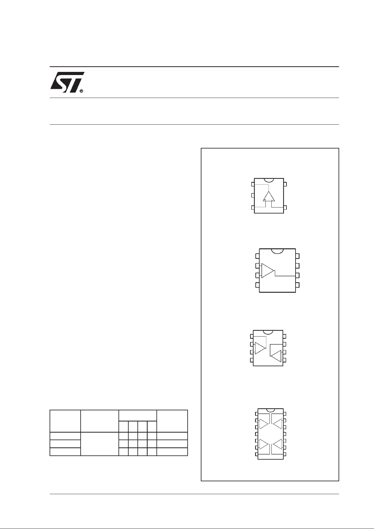
The TS1851 is housed in the space-saving 5 pin
SOT23-5 package which simplifies the board design (outside dimensions are 2.8mm x 2.9mm).
APPLICATION
■Two-cellbattery-powered systems
■Portable/Battery-powered electronic equipment
■Cordless phones
■Cellular phones
■Laptops
■PDAs
ORDER CODE
N=Dual in Line Package (DIP)
D=Small Outline Package (SO) - also available in Tape & Reel (DT)
P=Thin Shrink Small Outline Package (TSSOP) - only available
in Tape & Reel (PT)
L=Tiny Package (SOT23-5) -only available in Tape & Reel (LT)
PIN CONNECTIONS (top view)
Part
Number
Temperature
Range
Package
SOT23
Marking
NDPL
TS1851I/AI
-40, +125°C
••K161/K162
TS1852I/AI •••
TS1854I/AI •••
1
2
3
4
5
Inverting input
Non-inverting input
Output
V
DD
V
CC
1
2
3
4
5
6
7
8
-
+
Inve rting Input1
N.C.
Non-inve rting Inp ut 1
V
DD
V
CC
Output 2
N.C.
N.C.
Inverting Input 2
Non-inve rting Input 2
Non-inve rting Input1
DD
V
1
2
3
4
8
5
6
7
9
10
11
12
13
14
CC
V
Outp ut3
Outp ut4
Non-inve rting Input4
Inverting Inpu t 4
Non-inve rting Input3
Inverting Inpu t 3
-
+
+
-
+
-
+
Output1
Inve rting Input 1
Output2
1
2
3
45
6
7
8
-
+
-
+
Inve rting Input 1
Output 1
Non-inve rting Input 1
V
DD
V
CC
Output 2
Inverting Input 2
Non-inve rtingInput 2
TS1851ILT
TS1854IN-TS1854ID-TS1854IDT-TS1854IPT
TS1851ID-TS1851IDT
TS1852IN-TS1852ID-TS1852IDT-TS1852IPT
TS1851
TS1852
TS1854
1.8V INPUT/OUTPUT RAIL TO RAIL
LOW POWER OPERATIONAL AMPLIFIERS
May 2000
Page 2
TS1851-TS1852-TS1854
2/17
ABSOLUTE MAXIMUM RATINGS
OPERATING CONDITIONS
Symbol Parameter Value Unit
V
CC
Supply voltage
1)
7V
V
id Differential Input Voltage
2)
±1V
V
iInput Voltage
3)
-0.3 to VCC+0.3
V
T
oper
Operating Free Air Temperature Range -40 to + 125 °C
T
std
Storage Temperature -65 to +150 °C
T
j
Maximum Junction Temperature 150 °C
R
thjc Thermal Resistance Junction to Case
4)
SOT23-5
DIP8
DIP14
SO8
SO14
TSSOP8
TSSOP14
81
42
32
28
22
26
21
°C/W
R
thja
Thermal Resistance Junction to Ambient - SOT23-5 256 °C/W
ESD Human Body Model 2 kV
Lead Temperature (soldering, 10sec) 260 °C
1. All voltages values, except differential voltage are with respect to network terminal.
2. Differential voltages are non-inverting input terminal with respect to the inverting input terminal.
3. The magnitude of input and output voltages must never exceed V
CC
+0.3V.
4. Short-circuits can cause excessive heating. Destructive dissipation can result from simultaneous short-circuit on all amplifiers
Symbol Parameter Value Unit
V
CC
Supply Voltage 1.8 to 6 V
V
icm
Common Mode Input Voltage Range
1)
Vee-0.2 to VCC+ 0.2
V
V
icm Common Mode Input Voltage Range
2)
Veeto V
CC
V
1. At 25°C, for 1.8 ≤ VCC≤ 6V, V
icm
is extended to Vee- 0.2V, VCC+ 0.2V.
2. In full temperature range, bothRails can be reached when V
CC
does not exceed 5.5V.
Page 3
TS1851-TS1852-TS1854
3/17
ELECTRICAL CHARACTERISTICS
VCC= +1.8V,Vee= 0V,
T
amb
=25°C (unless otherwise specified)
Symbol Parameter Min. Typ. Max. Unit
V
io
Input Offset Voltage
TS1851/2/4
TS1851A/2A/4A
0.1 3
1
mV
∆V
io
Input Offset Voltage Drift 2 µV/°C
I
io
Input Offset Current
1)
1. Maximum values including unavoidable inaccuracies of the industrial test.
19nA
I
ib Input Bias Current
1)
10 50 nA
CMR
Common Mode Rejection Ratio
0 ≤ V
icm
≤ V
CC
55 85
dB
SVR
Supply Voltage Rejection Ratio
V
icm
= 0.5V
70 80 dB
A
vd
Large Signal Voltage Gain
R
L
= 1OkΩ
R
L
=2kΩ
80
70
100
88
dB
V
OH
High Level Output Voltage
R
L
= 10kΩ
R
L
=2kΩ
1.7
1.65
1.77
1.7
V
V
OL
Low Level Output Voltage
R
L
= 10kΩ
R
L
=2kΩ
40
62
70
90
mV
I
o
Output Source Current
V
ID
= 100mV, VO=V
DD
Output Sink Current
V
ID
= -100mV, VO=V
CC
2
2
29
46
mA
I
CC
Supply Current (per amplifier)
A
VCL
= 1, no load
120 170
µA
GBP
Gain Bandwith Product R
L
= 10kΩ,CL= 100pF, f = 100kHz
300 480 kHz
SR
Slew Rate R
L
= 10kΩ,CL= 100pF, AV= 1
0.1 0.18 V/µs
φm
Phase Margin C
L
= 100pF
60 Degrees
en Input Voltage Noise 40 nV/√Hz
THD Total Harmonic Distortion 0.01 %
Page 4
TS1851-TS1852-TS1854
4/17
ELECTRICAL CHARACTERISTICS
VCC= +3V,Vee= 0V,
T
amb
=25°C (unless otherwise specified)
Symbol Parameter Min. Typ. Max. Unit
V
io
Input Offset Voltage
TS1851/2/4
TS1851A/2A/4A
0.1 3
1
mV
∆V
io
Input Offset Voltage Drift 2 µV/°C
I
io
Input Offset Current
1)
1. Maximum values including unavoidable inaccuracies of the industrial test.
19nA
I
ib
Input Bias Current
1)
10 55 nA
CMR
Common Mode Rejection Ratio
0 ≤ V
icm
≤ V
CC
60 90
dB
SVR
Supply Voltage Rejection Ratio
V
icm=VCC/2
70 85
dB
A
vd
Large Signal Voltage Gain
R
L
= 1OkΩ
R
L
=2kΩ
83
74
99
90
dB
V
OH
High Level Output Voltage
R
L
= 10kΩ
R
L
=2kΩ
2.9
2.85
2.96
2.94
V
V
OL
Low Level Output Voltage
R
L
= 10kΩ
R
L
=2kΩ
10
46
90
100
mV
I
o
Output Source Current
V
ID
= 100mV, VO=V
DD
Output Sink Current
V
ID
= -100mV, VO=V
CC
2
2
47
47
mA
I
CC
Supply Current (per amplifier)
A
VCL
= 1, no load
150 200
µA
GBP
Gain Bandwith Product R
L
= 10kΩ,CL= 100pF, f = 100kHz
370 600 kHz
SR
Slew Rate R
L
= 10kΩ,CL= 100pF, AV= 1
0.12 0.2 V/µs
φm
Phase Margin C
L
= 100pF
60 Degrees
en Input Voltage Noise 40 nV/√Hz
THD Total Harmonic Distortion 0.01 %
Page 5
TS1851-TS1852-TS1854
5/17
ELECTRICAL CHARACTERISTICS
VCC= +5V,Vee= 0V,
T
amb
=25°C (unless otherwise specified)
Symbol Parameter Min. Typ. Max. Unit
V
io
Input Offset Voltage
TS1851/2/4
TS1851A/2A/4A
0.1 3
1
mV
∆V
io
Input Offset Voltage Drift 2 µV/°C
I
io
Input Offset Current
1)
19nA
I
ib Input Bias Current
1)
16 63 nA
CMR
Common Mode Rejection Ratio
0 ≤ V
icm
≤ V
CC
65 95
dB
SVR
Supply Voltage Rejection Ratio
V
icm=VCC/2
70 90
dB
A
vd
Large Signal Voltage Gain
R
L
= 1OkΩ
R
L
=2kΩ
85
77
97
93
dB
V
OH
High Level Output Voltage
R
L
= 10kΩ
R
L
=2kΩ
4.85
4.8
4.95
4.91
V
V
OL
Low Level Output Voltage
R
L
= 10kΩ
R
L
=2kΩ
40
80
180
200
mV
I
o
Output Source Current
V
ID
= 100mV, VO=V
DD
Output Sink Current
V
ID
= -100mV, VO=V
CC
2
2
48
48
mA
I
CC
Supply Current (per amplifier)
A
VCL
= 1, no load
162 220
µA
GBP
Gain Bandwith Product R
L
= 10kΩ,CL= 100pF, f = 100kHz
380 630 kHz
SR
Slew Rate R
L
= 10kΩ,CL= 100pF, AV= 1
0.13 0.25 V/µs
φm
Phase Margin C
L
= 100pF
60 Degrees
en Input Voltage Noise 40 nV/√Hz
THD Total Harmonic Distortion 0.01 %
1. Maximum values including unavoidable inaccuracies of the industrial test.
Page 6
TS1851-TS1852-TS1854
6/17
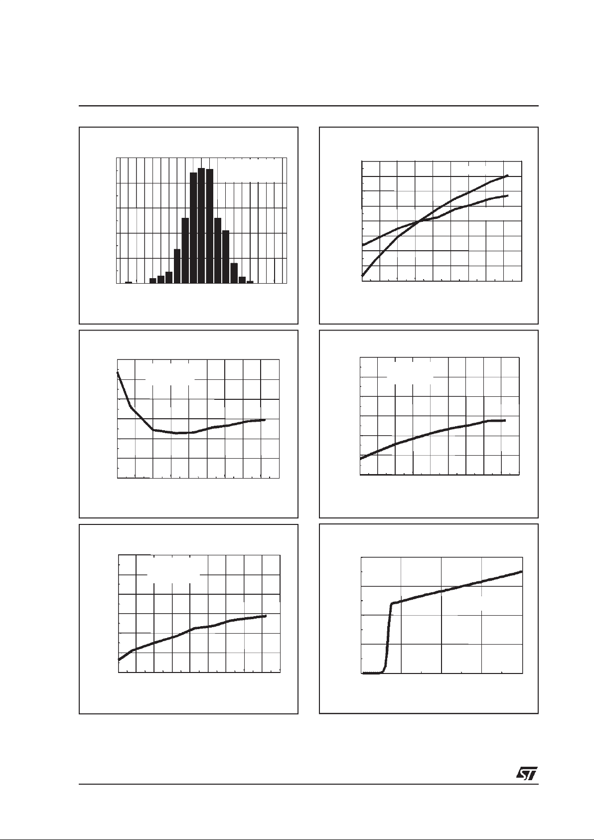
Input OffsetVoltage Distribution
-2. -1.6 -1.2 -.8 -.4 0 .4 .8 1.2 1.6 2
Input Offset Voltage (mV)
0
20
40
60
80
100
Quantity of Pieces
488 pieces tested
Vcc =10V
Temp = +25°C
InputBias Current vs Temperature
-40
-20
0
20
40
60
80
100
120
140
Temperature (°C)
-12
-10
-8
-6
-4
-2
0
Input biascurrent (nA)
Vcc = 1.8V
Vicm = 0.9V
Input Bias Current vs Temperature
-40
-20
0
20
40
60
80
100
120
140
Temperature (°C)
-12
-10
-8
-6
-4
-2
0
Input bias current (nA)
Vcc = 5V
Vicm = 2.5V
Input Offset VoltageDrift vs Temperature
-40
-20
0
20
40
60
80
100
120
140
Temperature (°C)
-400
-300
-200
-100
0
100
200
300
400
Input VoltageDrift (µV)
Vcc = 10V
Vcc = 1.8V
Input Bias Current vs Temperature
-40
-20
0
20
40
60
80
100
120
140
Temperature (°C)
-12
-10
-8
-6
-4
-2
0
Input bias current (nA)
Vcc =3V
Vicm = 1.5V
Supply Current/Amplifier vs Supply Voltage
02468
Supply Voltage (V)
0
50
100
150
200
Supply Current (µA)
Tamb = 25°C
Page 7

TS1851-TS1852-TS1854
7/17
SupplyCurrent/Amplifiervs Temperature
-40 -20 0 20 40 60 80 100 120 140
Temperature (°C)
90
100
110
120
130
140
150
160
170
Supply Current (µA)
Vcc = 1.8V
Vcc = 5V
Vcc = 3V
Common Mode Rejection vs Temperature
-50
0
50
100
150
Temperature (°C)
60
70
80
90
100
110
Common Mode Rejection (dB)
Vcc = 3V
SupplyVoltage Rejection vs Temperature
-40 -20 0 20 40 60 80 100 120 140
Temperature (°C)
60
70
80
90
100
110
Supply Voltage Rejection (dB)
Vcc = 2V
Vicm = 1V
Common Mode Rejection vs Temperature
-40 -20 0 20 40 60 80 100 120 140
Temperature (°C)
60
70
80
90
100
110
Common Mode Rejection (dB)
Vcc = 1.8V
Common Mode Rejection vs Temperature
-40 -20 0 20 40 60 80 100 120 140
Temperature (°C)
60
70
80
90
100
110
Common Mode Rejection (dB)
Vcc = 5V
Supply Voltage Rejection vs Temperature
-40
-20
0
20
40
60
80
100
120
140
Temperature (°C)
60
70
80
90
100
110
Supply Voltage Rejection (dB)
Vcc = 3V
Vicm = 1.5V
Page 8

TS1851-TS1852-TS1854
8/17
Supply Voltage Rejection vs Temperature
-40 -20 0 20 40 60 80 100 120 140
Temperature (°C)
60
70
80
90
100
110
Supply Voltage Rejection (dB)
Vcc = 5V
Vicm = 2.5V
Open LoopGain vs Temperature
-40
-20
0
20
40
60
80
100
120
140
Temperature (°C)
70
80
90
100
110
Open Loop Gain (dB)
Vcc = 3V
RL = 10 kohms
RL = 2 kohms
High Level Output Voltage vs Temperature
-40 -20 0 20 40 60 80 100 120 140
Temperature (°C)
20
25
30
35
40
45
50
55
Voltage Referenced to VCC (mV)
Vcc = 1.8V
Vcc = 3V
Vcc = 5V
RL = 10 kohms
Open Loop Gain vs Temperature
-40 -20 0 20 40 60 80 100 120 140
Temperature (°C)
70
80
90
100
110
Open Loop Gain (dB)
Vcc = 1.8V
RL = 10 kohms
RL = 2 kohms
Open Loop Gain vs Temperature
-40 -20 0 20 40 60 80 100 120 140
Temperature (°C)
70
80
90
100
110
Open Loop Gain (dB)
Vcc = 5V
RL = 10 kohms
RL = 2 kohms
High Level Output Voltage vs Temperature
-40 -20 0 20 40 60 80 100 120 140
Temperature (°C)
20
25
30
35
40
45
50
55
Voltage Referenced to Gnd (mV)
Vcc = 1.8V
Vcc = 3V
Vcc = 5V
RL = 10 kohms
Page 9

TS1851-TS1852-TS1854
9/17
High Level Output Voltage vs Temperature
-40 -20 0 20 40 60 80 100 120 140
Temperature (°C)
40
50
60
70
80
90
100
110
Voltage Referenced to VCC (mV)
Vcc = 1.8V
Vcc = 3V
Vcc = 5V
RL = 2 kohms
Output Current vs Temperature
-40
-20
0
20
40
60
80
100
120
140
Temperature (°C)
-60
-40
-20
0
20
40
60
80
Output Current (mA)
Isink, Vcc = 1.8V
Vid =1V
Isource,Vcc = 1.8V
Isink, Vcc = 3V
Isink, Vcc = 5V
Isource, Vcc= 3V
Isource, Vcc= 5V
Output Current vs Output Voltage
0.0 0.5 1.0 1.5 2.0
OutputVoltage (V)
-60
-40
-20
0
40
60
80
Output Current (mA)
sink
Vcc = 3V
Vid = 0.1V
Vicm = 1.5V
source
T=25°C
T = 125 °C
T = -40 °C
T = 125 °C
T=25°C
T = -40 °C
2.5 3.0
20
High Level Output Voltage vs Temperature
-40 -20 0 20 40 60 80 100 120 140
Temperature (°C)
40
50
60
70
80
90
100
110
Voltage Referenced to Gnd (mV)
Vcc = 1.8V
Vcc = 3V
Vcc = 5V
RL = 2 kohms
Output Current vs Output Voltage
0.0 0.5 1.0 1.5 2.0
Output Voltage (V)
-40
-30
-20
-10
0
10
20
30
40
50
60
Output Current (mA)
sink
Vcc= 1.8V
Vid = 0.1V
Vicm =0.9V
source
T=25°C
T =125 °C
T = 125 °C
T = -40 °C
T=25°C
T = -40 °C
OutputCurrent vs Output Voltage
0.0
1.0
2.0
3.0
4.0
5.0
Output Voltage (V)
-60
-40
-20
0
20
40
60
80
Output Current (mA)
sink
Vcc = 5V
Vid = 0.1V
Vicm =2.5V
source
T=25°C
T = -40 °C
T = 125 °C
T = 125 °C
T = -40 °C
T=25°C
Page 10

TS1851-TS1852-TS1854
10/17
Gain and Phasis vs
Frequency
1E+3 1E+4 1E+5 1E+6
Frequency(Hz)
0
10
20
30
40
50
60
70
Gain (dB)
40
60
80
100
120
140
160
180
Phase (°)
RL = 10K
CL = 100 pF
Vcc = 1.8V
gain
phase
Gain and Phasis vs Frequency
1E+3 1E+4 1E+5 1E+6
Frequency(Hz)
0
10
20
30
40
50
60
70
Gain (dB)
40
60
80
100
120
140
160
180
Phase (°)
RL = 10K
CL = 100 pF
Vcc = 5V
gain
phase
Gain-BandwithProduct vs Supply Voltage
01234567
Supply Voltage (V)
450
500
550
600
650
700
750
800
Gain-BandwithProduct (MHz)
RL = 2 kohms
CL = 300 pF
Vicm = Vcc/2
T=25°C
Gain and Phasisvs Frequency
1E+3 1E+4 1E+5 1E+6
Frequency (Hz)
0
10
20
30
40
50
60
70
Gain (dB)
40
60
80
100
120
140
160
180
Phase (°)
RL= 10K
CL= 100 pF
Vcc =3V
gain
phase
Gain-BandwithProductvs Temperature
-40 -20 0 20 40 60 80 100 120 140
Temperature(°C)
0.45
0.50
0.55
0.60
0.65
Gain-BandwithProduct (MHz)
Vcc = 1.8V
Vcc = 3V
Vcc = 5V
Vicm = Vcc/2
RL =10kohms
CL =100 pF
Slew Rate vs Temperature
-40 -20 0 20 40 60 80 100 120 140
Temperature(°C)
0.11
0.12
0.13
0.14
0.15
0.16
0.17
0.18
0.19
Slew Rate(V/µs)
positive Slew Rate
Vcc = 1.8V
gain = +1
Vin = 0.4to 1.4V
RL = 10kohms
CL = 100 pF
negative Slew Rate
Page 11

TS1851-TS1852-TS1854
11/17
Slew Rate vs Temperature
-40 -20 0 20 40 60 80 100 120 140
Temperature(°C)
0.12
0.13
0.14
0.15
0.16
0.17
0.18
0.19
0.20
0.21
Slew Rate(V/µs)
positive Slew Rate
Vcc = 3V
gain = +1
Vin =1 to 2V
RL =10kohms
CL =100 pF
negative Slew Rate
Phase Margin vs Load Capacitor
10 100 1000
10000
Load Capacitor (pF)
-10
0
10
20
30
40
50
60
70
Phase Margin (°)
Vcc = 3V
gain = -1
Equivalent input noise vs Frequency
1E+1 1E+2 1E+3 1E+4 1E+5
Frequency(Hz)
0
10
20
30
40
50
Equivalent Input Noise(nV/sqr(Hz))
Vcc = 1.8V
gain = 100
Rs = 100 ohms
SlewRate vs Temperature
-40 -20 0 20 40 60 80 100 120 140
Temperature(°C)
0.13
0.14
0.15
0.16
0.17
0.18
0.19
0.20
0.21
0.22
Slew Rate (V/µs)
positive Slew Rate
Vcc =5V
gain =+1
Vin =2 to 3V
RL =10kohms
CL =100 pF
negativeSlew Rate
Phase Margin vs Output Current
-10 -5 0 5 10
DC Output Current(mA)
55
60
65
70
75
80
85
Phase Margin (°)
Vcc = 3V
RL = 2 kohms
CL = 100 pF
Distortion vs Output Voltage
0.000 0.100 0.200 0.300 0.400 0.500 0.600 0.700 0.800
Output Voltage (V)
0.001
0.010
0.100
1.000
10.000
Distortion (%)
RL = 10kohms
Vcc = 1.8V
f = 1kHz
T=25°C
gain = -1
RL = 2kohms
Page 12

TS1851-TS1852-TS1854
12/17
Distortion vs Output Voltage
0.000 0.200 0.400 0.600 0.800 1.000 1.200
Output Voltage(V)
0.001
0.010
0.100
1.000
10.000
Distortion (%)
Vcc = 3V
f = 1kHz
RL = 10K
T=25°C
gain = -1
Distortion vs Frequency
1E+1 1E+2 1E+3 1E+4 1E+5
Frequency(Hz)
0.001
0.010
0.100
1.000
Distortion (%)
RL = 10kohms
Vcc = 3V
Vout = 2Vpp
T=25°C
gain = -1
RL = 2kohms
Distortion vs Output Voltage
0.000 0.500 1.000 1.500
2.000
Output Voltage(V)
0.001
0.010
0.100
1.000
10.000
Distortion(%)
RL = 10kohms
Vcc = 5V
f = 1kHz
T=25°C
gain = -1
RL = 2kohms
Page 13

TS1851-TS1852-TS1854
13/17
TS1851ID - TS1852ID
PACKAGE MECHANICAL DATA
8 PINS - PLASTIC MICROPACKAGE (SO)
Dim.
Millimeters Inches
Min. Typ. Max. Min. Typ. Max.
A 1.75 0.069
a1 0.1 0.25 0.004 0.010
a2 1.65 0.065
a3 0.65 0.85 0.026 0.033
b 0.35 0.48 0.014 0.019
b1 0.19 0.25 0.007 0.010
C 0.25 0.5 0.010 0.020
c1 45° (typ.)
D 4.8 5.0 0.189 0.197
E 5.8 6.2 0.228 0.244
e 1.27 0.050
e3 3.81 0.150
F 3.8 4.0 0.150 0.157
L 0.4 1.27 0.016 0.050
M 0.6 0.024
S8°(max.)
Page 14

TS1851-TS1852-TS1854
14/17
TS1852IPT
PACKAGE MECHANICAL DATA
8 PINS - THIN SHRINK SMALL OUTLINE PACKAGE
Dim.
Millimeters Inches
Min. Typ. Max. Min. Typ. Max.
A 1.20 0.05
A1 0.05 0.15 0.01 0.006
A2 0.80 1.00 1.05 0.031 0.039 0.041
b 0.19 0.30 0.007 0.15
c 0.09 0.20 0.003 0.012
D 2.90 3.00 3.10 0.114 0.118 0.122
E 6.40 0.252
E1 4.30 4.40 4.50 0.169 0.173 0.177
e 0.65 0.025
k0° 8°0° 8°
l 0.50 0.60 0.75 0.09 0.0236 0.030
L
L1
c
0.25mm
.010 inch
GAGE PLANE
E1
k
L
L1
E
SEATING
PLANE
A
A2
D
A1
b
5
8
4
1
PIN 1 IDENTIFICATION
e
Page 15

TS1851-TS1852-TS1854
15/17
TS1854ID
PACKAGE MECHANICAL DATA
14 PINS - PLASTIC MICROPACKAGE (SO)
Dim.
Millimeters Inches
Min. Typ. Max. Min. Typ. Max.
A 1.75 0.069
a1 0.1 0.2 0.004 0.008
a2 1.6 0.063
b 0.35 0.46 0.014 0.018
b1 0.19 0.25 0.007 0.010
C 0.5 0.020
c1 45° (typ.)
D (1) 8.55 8.75 0.336 0.344
E 5.8 6.2 0.228 0.244
e 1.27 0.050
e3 7.62 0.300
F (1) 3.8 4.0 0.150 0.157
G 4.6 5.3 0.181 0.208
L 0.5 1.27 0.020 0.050
M 0.68 0.027
S8°(max.)
Note : (1) D and F do not include mold flash or protrusions - Mold flash or protrusions shall not exceed 0.15mm (.066 inc) ONLY FOR DATA BOOK.
D
M
F
14
1
7
8
b
e3
e
E
LG
C
c1
A
a2
a1
b1
s
Page 16

TS1851-TS1852-TS1854
16/17
TS1854IPT
PACKAGE MECHANICAL DATA
14 PINS - THIN SHRINK SMALL OUTLINE PACKAGE
Dim.
Millimeters Inches
Min. Typ. Max. Min. Typ. Max.
A 1.20 0.05
A1 0.05 0.15 0.01 0.006
A2 0.80 1.00 1.05 0.031 0.039 0.041
b 0.19 0.30 0.007 0.15
c 0.09 0.20 0.003 0.012
D 4.90 5.00 5.10 0.192 0.196 0.20
E 6.40 0.252
E1 4.30 4.40 4.50 0.169 0.173 0.177
e 0.65 0.025
k0° 8°0° 8°
l 0.50 0.60 0.75 0.09 0.0236 0.030
c
E1
k
L
E
e
b
D
L1
A
A2
A1
Page 17

TS1851-TS1852-TS1854
17/17
Information furnished is believed to be accurate and reliable. However, STMicroelectronics assumes no responsibility for the
consequences of use of such information nor for any infringement of patents or other rights of third parties which may result from
its use. No license is granted by implication or otherwise under any patent or patent rights of STMicroelectronics. Specifications
mentioned in this publication are subject to change without notice. This publication supersedes and replaces all information
previously supplied. STMicroelectronics products are not authorized for use as critical components in life support devices or
systems withoutexpress written approval of STMicroelectronics.
The ST logo isa registered trademark of STMicroelectronics
2000 STMicroelectronics - Printed in Italy - All Rights Reserved
STMicroelectronics GROUP OF COMPANIES
Australia - Brazil - China - Finland - France - Germany - Hong Kong - India - Italy - Japan - Malaysia - Malta - Morocco
Singapore - Spain - Sweden - Switzerland - United Kingdom
http://www.st.com
TS1851ILT
PACKAGE MECHANICAL DATA
5 PINS - TINY PACKAGE (SOT23)
Dim.
Millimeters Inches
Min. Typ. Max. Min. Typ. Max.
A 0.90 1.20 1.45 0.035 0.047 0.057
A1 0 0.15 0.006
A2 0.90 1.05 1.30 0.035 0.041 0.051
B 0.35 0.40 0.50 0.014 0.016 0.020
C 0.09 0.15 0.20 0.004 0.006 0.008
D 2.80 2.90 3.00 0.110 0.114 0.118
D1 1.90 0.075
e 0.95 0.037
E 2.60 2.80 3.00 0.102 0.110 0.0118
F 1.50 1.60 1.75 0.059 0.063 0.069
L 0.10 0.5 0.60 0.004 0.014 0.024
K 0d 10d 0d 10d
L
C
E1
A2
A
A1
b
E
D
 Loading...