

Page 1
TRF8011
900-MHz RF TRANSMIT DRIVER
SLWS056B – FEBRUAR Y 1997 – REVISED OCTOBER 1997
D
Operates from 4.8–V Power Supply for
900–MHz Applications
D
Unconditionally Stable
D
Wide UHF Frequency Range: 800 MHz to
1000 MHz
D
24.5 dBm Typical Output Power
D
Linear Ramp Control
D
Transmit Enable/Disable Control
D
Advanced BiCMOS Processing Technology
for Low-Power Consumption, High
Efficiency, and Highly Linear Operation
D
Minimum of External Components
Required for Operation
D
Thermally Enhanced Surface-Mount
GND
GND
RFIN
GND
NC
VPC
GND
NC
V
BB
GND
NC – No internal connection
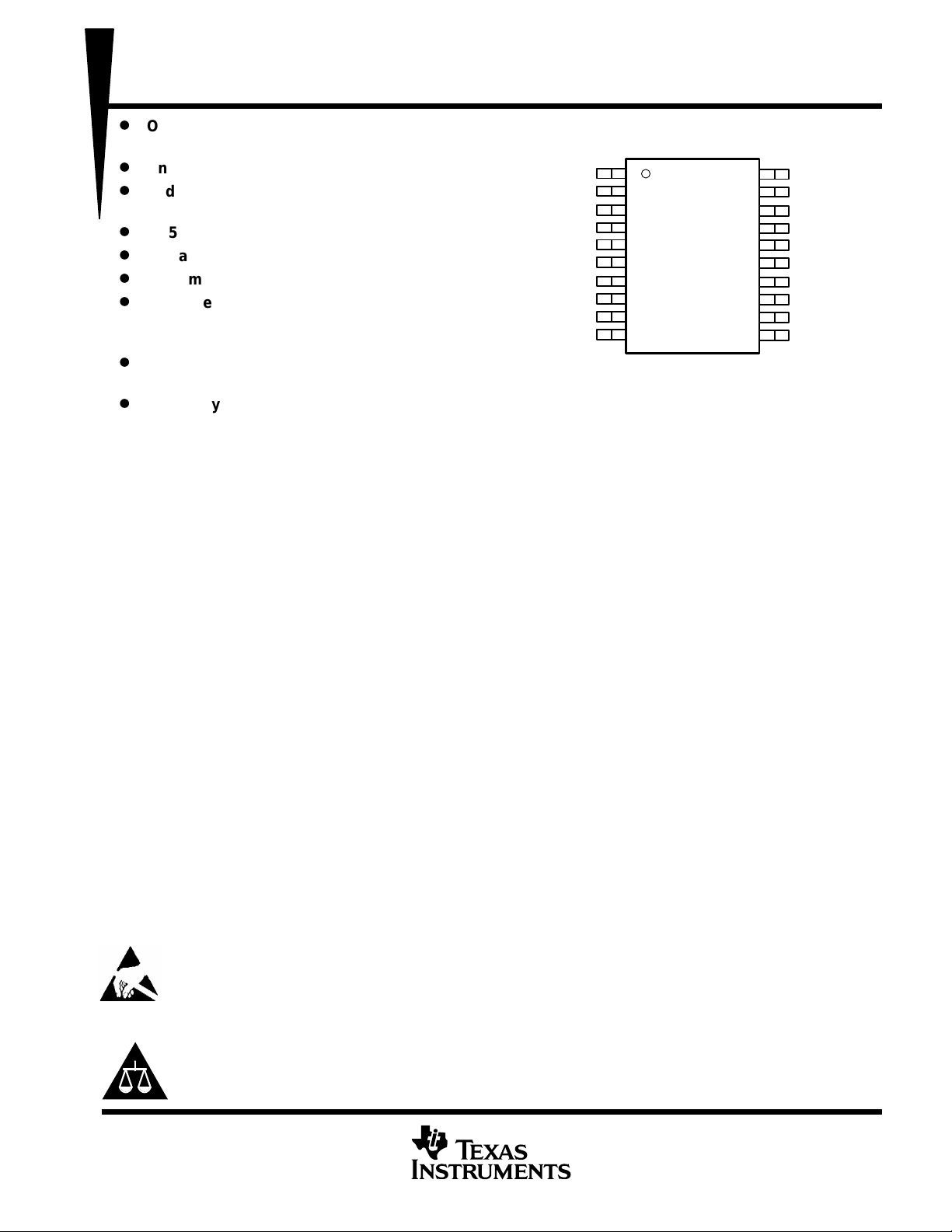
PWP PACKAGE
(TOP VIEW)
1
2
3
4
5
6
7
8
9
10
20
19
18
17
16
15
14
13
12
11
Package for Extremely Small Circuit
Footprint
description
The TRF8011 RF transmit driver amplifier is for use in 800 to 1000 MHz wireless communication systems. It
consists of a two-stage amplifier and a linear ramp controller for burst control in TDMA (time-division multiple
access) applications. Very few external components are required for operation. The input is dc-blocked and
requires no external matching. The output requires external matching suitable for the application frequency.
GND
GND
RFOUT
GND
GND
TXEN
GND
V
CC
V
CC
GND
The device is enabled when the TXEN input is held high. A power control signal applied to the VPC input can
ramp the RF output power up or down to meet ramp and spurious emission specifications in TDMA systems.
The power control signal causes a linear change in output power as the voltage applied to VPC varies between
0 V and 3 V. With the RF input power applied to RFIN at 5 dBm and TXEN high, adjusting VPC from 0 V to
3 V increases the output power from a typical value of –50 dBm to 24.5 dBm at 900 MHz. Forward isolation with
the input power applied to RFIN at 5 dBm, VPC = 0 V, and TXEN high is typically greater than 50 dB.
The TRF801 1 is available in a thermally enhanced, surface-mount, 20-pin PowerPAD
TM
(PWP) thin-shrink small
outline package (TSSOP) and is characterized for operation from –40°C to 85°C. The PWP package has a
solderable pad that can improve the package thermal performance by bonding the pad to an external thermal
plane. The pad also acts as a low-inductance electrical path to ground and must be electrically connected to
the PCB ground plane as a continuation of the regular package terminals that are designated GND.
These devices have limited built-in ESD protection. The leads should be shorted together or the device placed in conductive foam
during storage or handling to prevent electrostatic damage to the MOS gates.
Please be aware that an important notice concerning availability, standard warranty, and use in critical applications of
Texas Instruments semiconductor products and disclaimers thereto appears at the end of this data sheet.
PowerPAD is a trademark of Texas Instruments Incorporated.
PRODUCTION DATA information is current as of publication date.
Products conform to specifications per the terms of Texas Instruments
standard warranty. Production processing does not necessarily include
testing of all parameters.
POST OFFICE BOX 655303 • DALLAS, TEXAS 75265
Copyright 1997, Texas Instruments Incorporated
1
Page 2
TRF8011
I/O
DESCRIPTION
900-MHz RF TRANSMIT DRIVER
SLWS056B – FEBRUAR Y 1997 – REVISED OCTOBER 1997
functional block diagram
TXEN
VPC
3
15
6
Linear Ramp
Control
Bias/Band Gap
Reference
9 12, 13
VBBV
CC
18
RFOUTRFIN
Terminal Functions
TERMINAL
NAME NO.
GND 1,2,4,7,10,11,14,
NC 5, 8 No connection. It is recommended that all NC terminals be connected to ground.
RFIN 3 I RF input. RFIN accepts signals between 800 MHz and 1000 MHz.
RFOUT 18 O RF output. RFOUT is an open-collector output and requires a decoupled connection to VCC for
TXEN 15 I Transmit enable input (digital). When TXEN is high, the output device is enabled.
V
BB
V
CC
VPC 6 I V oltage power control. VPC is a signal between 0 V and 3 V that adjusts the output power from a typical
16,17,19,20
9 Control section supply voltage
12, 13 First stage bias
Analog ground for all internal circuits. All signals are referenced to the ground terminals.
operation.
value of –50 dBm to 25.5 dBm.
absolute maximum ratings over operating free-air temperature range (unless otherwise noted)
Supply voltage range, V
Input voltage range at TXEN, VPC –0.6 V to 5.6 V. . . . . . . . . . . . . . . . . . . . . . . . . . . . . . . . . . . . . . . . . . . . . . . . . .
Input power at RFIN 10 dBm. . . . . . . . . . . . . . . . . . . . . . . . . . . . . . . . . . . . . . . . . . . . . . . . . . . . . . . . . . . . . . . . . . . . .
Thermal resistance, junction to case, R
Thermal resistance, junction to ambient, R
Continuous total power dissipation at T
Operating junction temperature, T
Junction temperature T
Operating free-air temperature range, T
Storage temperature range, T
†
Stresses beyond those listed under “absolute maximum ratings” may cause permanent damage to the device. These are stress ratings only, and
functional operation of the device at these or any other conditions beyond those indicated under “recommended operating conditions” is not
implied. Exposure to absolute-maximum-rated conditions for extended periods may affect device reliability.
NOTES: 1. Voltage values are with respect to GND.
2. No air flow and with infinite heatsink
3. With the thermal pad of the device soldered to a 1-ounce copper (Cu) ground plane of an FR4 board with no air flow
(see Note 1) –0.6 V to 5.6 V. . . . . . . . . . . . . . . . . . . . . . . . . . . . . . . . . . . . . . . . . . . . . .
CC
(see Note 2) 3.5oC/W. . . . . . . . . . . . . . . . . . . . . . . . . . . . . . . . . . . . .
θJC
(see Note 3) 32oC/W. . . . . . . . . . . . . . . . . . . . . . . . . . . . . . . . . . .
θJA
= 25 oC 3.9 W. . . . . . . . . . . . . . . . . . . . . . . . . . . . . . . . . . . . . . . . . . . . . .
A
110oC. . . . . . . . . . . . . . . . . . . . . . . . . . . . . . . . . . . . . . . . . . . . . . . . . . . . . . . . .
stg
J
–40 oC to 85 oC. . . . . . . . . . . . . . . . . . . . . . . . . . . . . . . . . . . . . . . . . . .
A
–65 oC to 150 oC. . . . . . . . . . . . . . . . . . . . . . . . . . . . . . . . . . . . . . . . . . . . . . . . . . .
max 150oC. . . . . . . . . . . . . . . . . . . . . . . . . . . . . . . . . . . . . . . . . . . . . . . . . . . . . . . . . . . . . .
J
†
2
POST OFFICE BOX 655303 • DALLAS, TEXAS 75265
Page 3
Output
H
Noi
idth
TRF8011
900-MHz RF TRANSMIT DRIVER
SLWS056B – FEBRUAR Y 1997 – REVISED OCTOBER 1997
recommended operating conditions
MIN NOM MAX UNIT
Supply voltage: VCC (see Note 1) 3 5 V
High-level input voltage at TXEN, V
Low-level input voltage at TXEN, V
Operating free-air temperature, T
NOTE: 1. Voltage values are with respect to GND.
IH
IL
A
electrical characteristics over full range of operating conditions
PARAMETER TEST CONDITIONS MIN
Operating at maximum power out TXEN high, VPC = 3 V 190 200 210 mA
ICC Supply current from V
†
Typical values are at TA = 25°C
CC
Operating at minimum power out TXEN high, VPC = 0 V 10 mA
Power down TXEN low, VPC = 0 V 0.05 mA
VCC = 4.8 V, TXEN high, VPC = 3 V, TA = 25°C (unless otherwise noted)
PARAMETER TEST CONDITIONS
Operating frequency range 870 925 MHz
p
p
power
Gain (small signal) PI = –20 dBm 29 dB
Power added efficiency (PAE) PI = 5 dBm 31 %
Input return loss (internally matched) PI = –20 dBm 12 dB
2f
armonics
p
se power in 30 kHz bandw
0
3f
0
10 MHz above f0PI = 5 dBm –92 dBm
20 MHz above f0PI = 5 dBm –93 dBm
PI = 5 dBm 23.5 24.5 25.5 dBm
PI = 5 dBm, VPC = 0 V –50 dBm
PI = 5 dBm –20 dBc
PI = 5 dBm –35 dBc
VCC – 0.8 V
0.8 V
–40 85 °C
†
TYP
MIN TYP MAX UNIT
MAX UNIT
stability
PARAMETER TEST CONDITIONS MIN TYP MAX UNIT
Stability
‡
VSWR = voltage standing wave ratio
§
No parasitic oscillations (all spurious < –70 dBc)
switching characteristics
= 4.8 V, TA = 25°C
V
CC
PARAMETER TEST CONDITIONS
t
on
t
off
Switching time, RF output OFF to ON TXEN = high, VPC stepped from 0 V to 3 V 1 µs
Switching time, RF output ON to OFF TXEN = high, VPC stepped from 3 V to 0 V 2 µs
Output VSWR‡ < 6:1 all phases,
VCC < 5.6 V, PI = 5 dBm, Output power 25 dBm,
Output frequency band : 200 MHz – 1200 MHz
§
MIN TYP MAX UNIT
POST OFFICE BOX 655303 • DALLAS, TEXAS 75265
3
Page 4

TRF8011
900-MHz RF TRANSMIT DRIVER
SLWS056B – FEBRUAR Y 1997 – REVISED OCTOBER 1997
APPLICATION INFORMATION
A typical application example for GSM cellular telephone systems is shown in Figure 1.
In all cases, a capacitor must be connected from the positive power supply to ground, as close as possible to
the IC terminals for power supply bypassing. A dc-blocking capacitor is also required on the RF output. A list
of components and their functions is given in Table 1.
Board Material
Type FR4, er = 4.3, h = 12 mils
1
GND
GND
20
RF INPUT
V
CC
C4
R1
50 Ω
Line
10
2
GND
3
RFIN
4
GND
5
NC
6
VPC
7
GND
8
NC
9
V
BB
GND
RFOUT
GND
GND
GND
TXEN
GND
V
CC
V
CC
GND
19
18
17
16
15
14
13
12
11
L1
C1
50 Ω
Line
L = 200 Mils
50 Ω
Line
C3
L2
C2
RF OUTPUT
50 Ω
Line
Figure 1. Typical GSM Cellular Telephone Application
Table 1. External Component Selection
COMPONENT DESIGNATION TYPICAL VALUE FUNCTION
C1 4 pF Output impedance matching capacitor
C2 100 pF DC-blocking capacitor for RF output
C3 1000 pF Matching capacitor
C4 1 µF Power supply decoupling capacitor
L1 3.3 nH Output impedance matching inductor
L2 100 nH DC bias/RF choke
R1 80 Ω Bias supply resistor
4
POST OFFICE BOX 655303 • DALLAS, TEXAS 75265
Page 5

y
TRF8011
900-MHz RF TRANSMIT DRIVER
SLWS056B – FEBRUAR Y 1997 – REVISED OCTOBER 1997
TYPICAL CHARACTERISTICS
25
20
15
10
– Output Power – dBm
O
P
5
0
–20 –15 –10 –5
OUTPUT POWER
vs
INPUT POWER
–40°C
25°C
85°C
VCC = 4.8 V
VPC = 3 V
f = 900 MHz
0510
PI – Input Power – dBm
Figure 2
POWER ADDED EFFICIENCY
35
VCC = 4.8 V
VPC = 3 V
30
f = 900 MHz
25
20
15
10
PAE – Power Added Efficiency – %
5
0
–20 –15 –10 –5
vs
INPUT POWER
–40°C
85°C
0510
PI – Input Power – dBm
Figure 3
25°C
OUTPUT POWER AND POWER
ADDED EFFICIENCY
27.5
27
26.5
26
25.5
25
– Output Power – dBmP
O
24.5
VCC = 4.8 V
24
VPC = 3 V
PI = 5 dBm
23.5
860 870 880 890 900
–40°C
25°C
85°C
f – Frequency – MHz
vs
FREQUENCY
–40°C
25°C
85°C
Figure 4
P
O
PAE
910 920 930
35
30
25
20
15
10
5
0
– %
– Output Power – dBmP
PAE – Power Added Efficienc
VPC GAIN CONTROL RANGE
30
PI = 5 dBm
VCC = 4.8 V
20
f = 900 MHz
10
0
–10
–20
O
–30
–40
–50
0 0.5 1 1.5
VPC – Power Control Input – V
OUTPUT POWER
vs
85°C
25°C
Figure 5
–40°C
2 2.5 3
POST OFFICE BOX 655303 • DALLAS, TEXAS 75265
5
Page 6

TRF8011
900-MHz RF TRANSMIT DRIVER
SLWS056B – FEBRUAR Y 1997 – REVISED OCTOBER 1997
TYPICAL CHARACTERISTICS
INPUT RETURN LOSS
–11
–11.5
–12
Input Return Loss – dB
–12.5
vs
FREQUENCY
VCC = 4.8 V
VPC = 3 V
PI = –20 dBm
85°C
25°C
–40°C
–13
860 870 880 890 900
f – Frequency – MHz
Figure 6
910 920 930
940
6
POST OFFICE BOX 655303 • DALLAS, TEXAS 75265
Page 7

TRF8011
900-MHz RF TRANSMIT DRIVER
SLWS056B – FEBRUAR Y 1997 – REVISED OCTOBER 1997
MECHANICAL DATA
PWP (R-PDSO-G**) PowerPAD PLASTIC SMALL-OUTLINE PACKAGE
0,65
20
1
1,20 MAX
0,30
0,19
11
4,50
4,30
10
A
Seating Plane
0,15
0,05
M
0,10
Thermal Pad (3,18 2,41 NOM)
(see Note C)
6,60
6,20
0,10
0,15 NOM
Gage Plane
0,25
0°–8°
0,75
0,50
PINS **
DIM
A MAX
A MIN
NOTES: A. All linear dimensions are in millimeters.
B. This drawing is subject to change without notice.
C. The package thermal performance may be enhanced by bonding the thermal pad to an external thermal plane. This solderable pad
is electrically and thermally connected to the backside of the die and leads 1, 10, 11, and 20.
PowerPAD is a trademark of Texas Instruments Incorporated.
5,10
14
16
5,10
4,904,90
20
6,60
6,40
24
7,90
28
9,80
9,607,70
4073225/E 03/97
POST OFFICE BOX 655303 • DALLAS, TEXAS 75265
7
Page 8

IMPORTANT NOTICE
T exas Instruments (TI) reserves the right to make changes to its products or to discontinue any semiconductor
product or service without notice, and advises its customers to obtain the latest version of relevant information
to verify, before placing orders, that the information being relied on is current.
TI warrants performance of its semiconductor products and related software to the specifications applicable at
the time of sale in accordance with TI’s standard warranty. Testing and other quality control techniques are
utilized to the extent TI deems necessary to support this warranty. Specific testing of all parameters of each
device is not necessarily performed, except those mandated by government requirements.
Certain applications using semiconductor products may involve potential risks of death, personal injury, or
severe property or environmental damage (“Critical Applications”).
TI SEMICONDUCTOR PRODUCTS ARE NOT DESIGNED, INTENDED, AUTHORIZED, OR WARRANTED
TO BE SUITABLE FOR USE IN LIFE-SUPPORT APPLICATIONS, DEVICES OR SYSTEMS OR OTHER
CRITICAL APPLICATIONS.
Inclusion of TI products in such applications is understood to be fully at the risk of the customer. Use of TI
products in such applications requires the written approval of an appropriate TI officer . Questions concerning
potential risk applications should be directed to TI through a local SC sales office.
In order to minimize risks associated with the customer’s applications, adequate design and operating
safeguards should be provided by the customer to minimize inherent or procedural hazards.
TI assumes no liability for applications assistance, customer product design, software performance, or
infringement of patents or services described herein. Nor does TI warrant or represent that any license, either
express or implied, is granted under any patent right, copyright, mask work right, or other intellectual property
right of TI covering or relating to any combination, machine, or process in which such semiconductor products
or services might be or are used.
Copyright 1998, Texas Instruments Incorporated
 Loading...