

Page 1
DUAL-BAND/DUAL-MODE PCS RECEIVER
SLWS041A – JANUARY 1998
D
Low-Noise Amplifier for Each Band
D
RF Mixer for Each Band With Image
Rejection Configuration for High Band
D
IF Amplifier for Both Low and High Bands
D
Operates From a Supply Voltage Range of
3.6 V to 4 V
description
The TRF1500 is a dual-band/dual-mode personal communications system (PCS) receiver for cellular
telephones operating dual mode (analog and digital) in the 800-MHz band and single mode (digital) in the
1900-MHz band.
uses an image rejection mixer for down conversion while the low band relies on an off-chip image rejection filter
between the LNA and mixer.
The local oscillator (LO) inputs additionally have buffered outputs that can be used in either single-ended or
differential mode for a phase-locked-loop (PLL) configuration. A state is also available that allows the low-band
LO to serve as the high-band LO through a mode-selectable frequency doubler.
A wideband mixer is also available for transmit loop architectures commonly used in advanced mobile phone
systems, global systems for mobile communications, and digital cellular systems.
The TRF1500 consists of a low-noise amplifier (LNA) and mixer for each band. The high band
D
Suitable for Portable Dual-Band/Dual-Mode
Cellular Telephones (IS136)
D
48-Pin Plastic Thin Quad Flatpack Package
(TQFP)
TRF1500
Power consumption is low and can be further reduced by operating the TRF1500 in sleep mode. Typical power
consumption for each receiver function is shown in Table 1.
The TRF1500 is available in a 48-pin plastic thin-quad flatpack package (TQFP) and is characterized for
operation from –30
_
C to 85 _C operating free-air temperature.
Table 1. Typical Power Consumption at V
FUNCTION TYPICAL POWER UNIT
Sleep mode 38 µW
Low band 85 mW
High band 190 mW
Transmit mixer 50 mW
Frequency doubler 12 mW
= 3.75 V
CC
These devices have limited built-in ESD protection. The leads should be shorted together or the device placed in conductive foam
during storage or handling to prevent electrostatic damage to the MOS gates.
Please be aware that an important notice concerning availability, standard warranty, and use in critical applications of
Texas Instruments semiconductor products and disclaimers thereto appears at the end of this data sheet.
PRODUCTION DATA information is current as of publication date.
Products conform to specifications per the terms of Texas Instruments
standard warranty. Production processing does not necessarily include
testing of all parameters.
POST OFFICE BOX 655303 • DALLAS, TEXAS 75265
Copyright 1997, Texas Instruments Incorporated
1
Page 2
TRF1500
DUAL-BAND/DUAL-MODE PCS RECEIVER
SLWS041A – JANUARY 1998
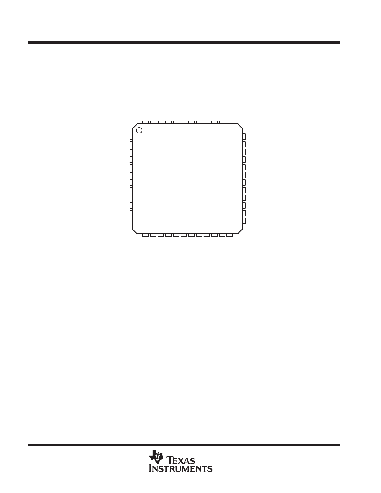
IR_ADJUST_C
GND
GND
47 46 45 44 4348 42
BIAS_ADJUST
TX_IF +
TX_IF –
GND
MIX_IN_LOW_BAND
GND
GND
TX +
TX –
GND
IR_ADJUST_D
1
2
3
4
5
6
V
7
CC
8
9
10
11
12
14 15
13
16
PFB PACKAGE
(TOP VIEW)
CC
GND
LOW_BAND_LNA_IN
HIGH_BAND_LNA_IN
GND
LOW_BAND_LNA_OUT
17 18 19 20
GND
40 39 3841
21
STRONG_SIGNAL
V
22 23 24
IR_ADJUST_B
37
36
IR_ADJUST_A
35
X2_ON
34
GND
33
GND
32
LOW_BAND_LO_IN
31
V
CC
30
DOUBLER_TANK
29
GND
28
HIGH_BAND_LO_IN +
27
HIGH_BAND_LO_IN –/RF_GND
TX_ON
26
V
25
CC
HI/LO
SYN_ON
HIGH_BAND_IF–
HIGH_BAND_IF+
GND
LOW_BAND_IF–
LOW_BAND_IF+
HIGH_BAND_LO–
HIGH_BAND_LO+
RX_ON
LOW_BAND_LO–
LOW_BAND_LO+
2
POST OFFICE BOX 655303 • DALLAS, TEXAS 75265
Page 3
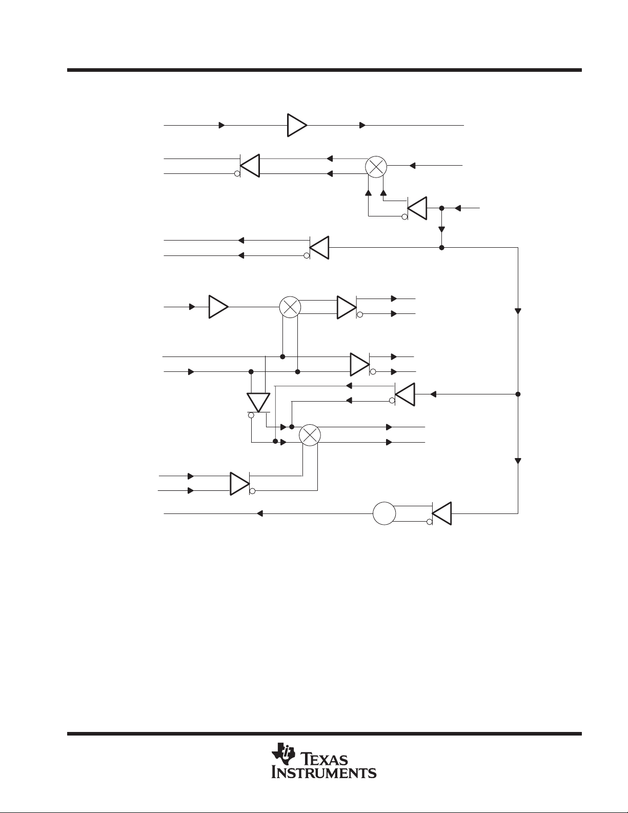
functional block diagram
LOW BAND LNA IN
LOW BAND IF +
LOW BAND IF –
LOW BAND LO +
LOW BAND LO –
43
17
18
22
23
Low
Low-Band IF
Buffer Amplifier
-Band LNA
Low-Band LO
Buffer Amplifier
TRF1500
DUAL-BAND/DUAL-MODE PCS RECEIVER
SLWS041A – JANUARY 1998
45
LOW BAND LNA OUT
Low
-Band
Mixer
5
MIX IN LOW BAND
Low-Band LO
Buffer Amplifier
32
LOW BAND LO IN
HIGH BAND LNA IN
HIGH BAND LO IN –
/RF GND
HIGH BAND LO IN +
TX +
TX –
DOUBLER
TANK
42
27
28
10
30
High-Band
LNA
Buffer
Amplifier
9
Amplifier
Image Reject Mixer
Buffer
High-Band IF
Buffer Amplifier
High-Band LO
Buffer Amplifier
Transmit
Mixer
Buffer
Amplifier
Doubler
15
HIGH BAND IF +
16
HIGH BAND IF –
20
HIGH BAND LO +
21
HIGH BAND LO –
2
TX IF +
3
TX IF –
Buffer
Amplifier
× 2
POST OFFICE BOX 655303 • DALLAS, TEXAS 75265
3
Page 4
TRF1500
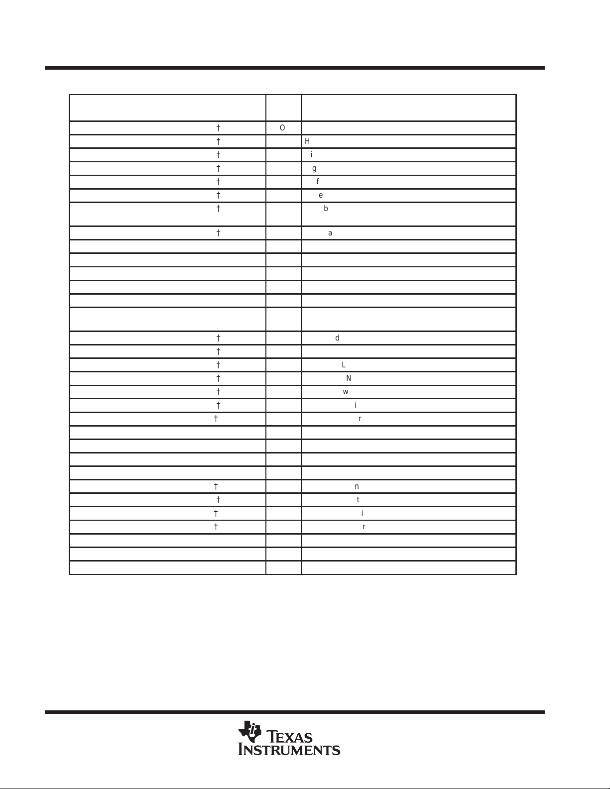
I/O
DESCRIPTION
DUAL-BAND/DUAL-MODE PCS RECEIVER
SLWS041A – JANUARY 1998
Terminal Functions
TERMINAL
NAME NO.
DOUBLER_TANK 30
HIGH_BAND_IF + 15
HIGH_BAND_IF – 16
HIGH_BAND_LNA_IN 42
HIGH_BAND_LO + 20
HIGH_BAND_LO – 21
HIGH_BAND_LO_IN –
/RF_GND
HIGH_BAND_LO_IN + 28
HI/LO 13 I High-band/low-band select; 1 = high band, 0 = low band
IR_ADJUST_A 36 I Image rejection adjustment
IR_ADJUST_B 37 I Image rejection adjustment
IR_ADJUST_C 48 I Image rejection adjustment
IR_ADJUST_D 12 I Image rejection adjustment
GND 4, 6, 8, 11, 19, 29, 33, 34,
LOW_BAND_IF + 17
LOW_BAND_IF – 18
LOW_BAND_LNA_IN 43
LOW_BAND_LNA_OUT 45
LOW_BAND_LO – 23
LOW_BAND_LO_IN 32
MIX_IN_LOW_BAND 5
BIAS_ADJUST 1 I Bias adjustment
RX_ON 24 I Receiver LNA/mixer power control
STRONG_SIGNAL 38 I Strong signal indication
SYN_ON 14 I VCO power control
TX + 9
TX – 10
TX_IF + 2
TX_IF – 3
TX_ON 26 I Transmit mixer/driver power control
V
CC
X2_ON 35 I Doubler power control
†
Pins without internal ESD protection
39, 41, 44, 46, 47
{
{
{
{
{
{
27
{
{
{
{
{
{
{
{
{
{
{
{
{
7, 25, 31, 40 I V
O Doubler output
O High-band IF noninverting output
O High-band IF inverting output
I High-band LNA input
O Buffered high-band LO noninverting output
O Buffered high-band LO inverting output
I High-band LO inverting input/RF GND
I High-band LO noninverting input
O Low-band IF noninverting output
O Low-band IF inverting output
I Low-band LNA input
O Low-band LNA output
O Buffered low-band LO inverting output
I Low-band LO input
I Low-band mixer input
I Transmit, noninverting input
I Transmit, inverting input
O Transmit IF, noninverting output
O Transmit IF, inverting output
Ground
CC
4
POST OFFICE BOX 655303 • DALLAS, TEXAS 75265
Page 5
TRF1500
DUAL-BAND/DUAL-MODE PCS RECEIVER
SLWS041A – JANUARY 1998
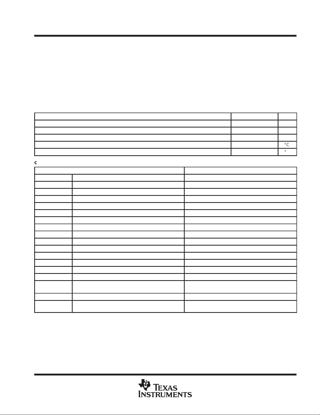
absolute maximum ratings over operating free-air temperature range (unless otherwise noted)
Supply voltage range, V
Power dissipation, T
Maximum operating junction temperature, T
Operating free-air temperature range, T
Storage temperature range, T
†
Stresses beyond those listed under “absolute maximum ratings” may cause permanent damage to the device. These are stress ratings only, and
functional operation of the device at these or any other conditions beyond those indicated under “recommended operating conditions” is not
implied. Exposure to absolute-maximum-rated conditions for extended periods may affect device reliability.
–0.3 V to 6 V. . . . . . . . . . . . . . . . . . . . . . . . . . . . . . . . . . . . . . . . . . . . . . . . . . . . . . . . . .
CC
= 25°C 350 mW. . . . . . . . . . . . . . . . . . . . . . . . . . . . . . . . . . . . . . . . . . . . . . . . . . . . . . . . . . . . .
A
–40°C to 85°C. . . . . . . . . . . . . . . . . . . . . . . . . . . . . . . . . . . . . . . . . . . .
–65°C to 150°C. . . . . . . . . . . . . . . . . . . . . . . . . . . . . . . . . . . . . . . . . . . . . . . . . . .
stg
A
150°C. . . . . . . . . . . . . . . . . . . . . . . . . . . . . . . . . . . . . . . . . . . . .
Jmax
recommended operating conditions
MIN NOM MAX UNIT
Supply voltage, V
High-level input voltage, V
Low-level input voltage, V
Operating free-air temperature, T
Operating junction temperature, T
CC
IH
IL
A
J
control state
CONTROL STATE (HI/L0, SYN ON, RX ON, TX ON, STRONG SIGNAL, X2) ACTIVE CIRCUITS
000000 Sleep mode
010000 Low-band LO input buffer on LB LO buffer
011000 Low-band receive normal LB LO buffer, LB LNA, LB mixer
011010 Low-band receive strong signal LB LO buffer,LB mixer
010100 Low-band transmit mixer LB LO buffer, LB TX mixer
011100 Low-band receive and transmit mixer LB LO buffer, LB LNA (on high), LB mixer, LB TX mixer
011110 Low-band transmit LB LO buffer, LB LNA (on high), LB mixer
010001 Double on LB LO buffer, doubler, HB LO buffer
011001 LB Receive normal, doubler on LB LO buffer, LB LNA, LB mixer, doubler
011011 LB receive strong signal, doubler on LB LO buffer, LB mixer, doubler
011111 LB transmit, doubler on LB LO buffer, LB LNA (on high), LB mixer, LB TX mixer
111011 High–band receive strong signal HB LO buffer, HB mixer, doubler
110000 High-band LO input buffer on HB LO buffer
111000 High-band receive normal HB LO buffer, HB LNA, HB mixer
111010 High-band receive strong signal HB LO buffer, HB mixer
111001 High-band receive frequency doubler on LB LO buffer, HB LNA, HB mixer, frequency doubler, HB
110100 High-band transmit normal HB LO buffer, HB TX mixer
110101 High-band transmit frequency doubler on LB LO buffer, HB TX mixer, frequency doubler, HB LO
LO buffer
buffer
3.6 3.75 4 V
3 V
–0.3 0.5 V
–30 85
–30 105
CC
V
_
C
_
C
†
POST OFFICE BOX 655303 • DALLAS, TEXAS 75265
5
Page 6
TRF1500
DUAL-BAND/DUAL-MODE PCS RECEIVER
SLWS041A – JANUARY 1998
current consumption, VCC = 3.75 V, TA = 25°C
CONTROL STATE (HI/L0, SYN ON, RX ON, TX ON, STRONG SIGNAL, X2) MIN TYP MAX UNIT
000000 Sleep mode 20 100 µA
010000 Low-band LO input buffer on 3.3 4 mA
011000 Low-band receive normal 24 28 mA
110000 High-band LO input buffer on 4 5 mA
111000 High-band receive normal 56 62 mA
111001 High–band receive with doubler on 61 68 mA
010100 Low-band transmit mixer 13 16 mA
110100 High-band transmit mixer 17 21 mA
110101 High-band transmit mixer, doubler on 22 27 mA
electrical characteristics at 881.5 MHz (unless otherwise noted)
low-band LNA, mixer, saw filter, and IF buffer amplifier, VCC = 3.75 V†, TA = 25°C
PARAMETER
RF input frequency range 869 894 MHz
LO frequency range 979.52 1004.52 MHz
IF frequency 110.52 MHz
LO input power –5 dBm
Turn on/off time 65 µs
Power conversion gain 24 26 28 dB
Power conversion gain reduction Strong signal condition: LNA off 19 dB
Noise figure 2.5 3.0 dB
RF input return loss Z= 50 Ω 5.6 dB
LO input return loss 16.5 dB
LO buffer output power –10.3 dBm
Power leakage LO in to RF in –53 dBm
IIP3 (third-order intermodulation product) Referenced RF input port –9.7 dBm
1-dB RF input compression point Referenced RF input port –21 dBm
1-dB blocking point Blocking signal 45 MHz below f
†
Low-band LNA, mixer, and IF amplifier with an external surface-acoustic wave (SA W) filter having 3-dB insertion loss (IL). All specifications apply
for an IF output terminated into a 1-kΩ load. Parametric limits apply only when tested using the evaluation board or the recommended application
circuit.
TEST CONDITIONS
MIN TYP MAX UNIT
0
–18 dBm
6
POST OFFICE BOX 655303 • DALLAS, TEXAS 75265
Page 7

TRF1500
DUAL-BAND/DUAL-MODE PCS RECEIVER
SLWS041A – JANUARY 1998
electrical characteristics at 1960 MHz (unless otherwise noted)
high-band LNA, mixer, and IF buffer amplifier, doubler, VCC = 3.75 V†, TA = 25°C
PARAMETER
RF input frequency range 1930 1990 MHz
LO frequency range (at doubler input) 1020.26 1050.26 MHz
IF frequency 110.52 MHz
LO input power –5 dBm
Power conversion gain 24 26.3 29 dB
Power conversion gain reduction Strong signal condition: LNA off 43.5 dB
Image Rejection 20 22.5 dB
Noise figure 4.66 5.1 dB
Noise figure Control state 111000,
RF input return loss 50 Ω 14.2 dB
LO buffer output power –14 dBm
Power leakage LO in to RF in –50 dBm
IIP3 (third-order intermodulation product) Referenced RF input port –19 –17.7 dBm
1-dB RF input compression point Referenced RF input port –23.7 dBm
2 x 2 spur performance
3 x 3 spur performance
†
High-band LNA, mixer, and IF amplifier specifications apply for an IF output terminated into a 1-k Ω load. Parametric limits apply only when tested
using the evaluation board or recommended application circuit using the internal frequency doubler.
TEST CONDITIONS
LOFR=2070.52
–50 dBm referenced RF input
port,
LO=1020.13 MHz and RF=1985
–50 dBm referenced RF input
port,
LO=1019.92 MHz and RF=2003
MIN TYP MAX UNIT
4.35
69 dBc
81 dBc
dB
electrical characteristics at 836.5 MHz (unless otherwise noted)
low-band transmit mixer, VCC = 3.75 V}, TA = 25°C
PARAMETER TEST CONDITIONS MIN TYP MAX UNIT
TX mixer input frequency 824 849 MHz
LO frequency 941 966 MHz
TX mixer output frequency 117 MHz
LO input power –5 dBm
Conversion power gain 17 19 dB
Noise figure Double sideband 7.8 dB
TX input return loss Balanced 200 Ω 9.8 dB
Power leakage LO in to TX in –49 dBm
Power leakage TX in to LO in TX In = –30 dBm –70.6 dBm
1-db input compression point Referred to TX input –20 dBm
Second-order input intercept point (IIP2) Referred to TX input 29.5 dBm
Third-order input intercept point (IIP3) Referred to TX input –11.5 dBm
‡
Transmit mixer specifications apply for an IF output terminated into a 1-kΩ resistor load.
POST OFFICE BOX 655303 • DALLAS, TEXAS 75265
7
Page 8

TRF1500
DUAL-BAND/DUAL-MODE PCS RECEIVER
SLWS041A – JANUARY 1998
electrical characteristics at 1910 MHz (unless otherwise noted)
high-band transmit mixer, doubler, VCC = 3.75 V†, TA = 25°C
PARAMETER TEST CONDITIONS MIN TYP MAX UNIT
TX mixer input frequency 1850 1910 MHz
LO frequency 983.8 1013.5 MHz
TX mixer output frequency 117 MHz
LO input power –5 dBm
Conversion power gain 6 9.9 dB
Noise figure Double sideband 12.7 dB
TX input return loss Balanced 200 Ω 16.6 dB
Power leakage LO in to TX in –55.5 dBm
Power leakage TX in to LO in TX In = –30 dBm –69.5 dBm
1-db input compression point Referred to TX input –15.7 dBm
Second-order input intercept point (IIP2) Referred to TX input 27 dBm
Third-order input intercept point (IIP3) Referred to TX input –6.7 dBm
†
High-band transmit mixer specifications apply for an IF output terminated into a 1-kΩ resistor load using the internal frequency doubler.
8
POST OFFICE BOX 655303 • DALLAS, TEXAS 75265
Page 9

J10 J20
TRF1500
DUAL-BAND/DUAL MODE PCS RECEIVER
SLWS041A – JANUARY 1998
APPLICATION INFORMATION
CC
V
C4
X2_ON
STR_SIG
36
V
GND
GND
GND
GND
GND
IR_AD–
JUST_A
BIAS_
1
C50
35
ADJUST
2
C32
L50
X2_ON
IR_ADJUST_B
STRONG_SIGNAL
IR_ADJUST_C
TX_IF+
T31
CC
V
37
C1
C20
L20
C29
C10
L10
C11
38
39
CC
40
41
CC
V
42
R7
43
R6
44
45
46
47
48
CC
V
L31 L30
C34
J31
C17 J12
34
33
32
GND
GND
LOW_BAND_LO_IN
HIGH_BAND_LNA_IN
LOW_BAND_LNA_IN
LOW_BAND_LNA_OUT
TX_IF–
GND
MIX_IN_LOW_BAND
3
4
5
C13
C33
F10
L40
L14
31
30
CC
V
TRF1500
CC
V
GND
6
7
CC
V
L11
J22
C41
C40
29
28
GND
DOUBLER_TANK
HIGH_BAND_LO_IN+
GND
8
9
C2
C30
C24
TX_ON
27
26
TX_ON
/RF_GND
HIGH_BAND_LO_IN–
TX+
TX–
GND
11
10
C31
T30
J30
CC
V
C3
25
CC
V
IR_ADJUST_D
12
C35 C36
J50
C26
RX_ON
RX_ON
24
LOW_BAND_LO–
23
LOW_BAND_LO+
22
HIGH_BAND_LO–
21
HIGH_BAND_LO+
20
GND
19
LOW_BAND_IF–
18
LOW_BAND_IF+
17
HIGH_BAND_IF–
16
HIGH_BAND_IF+
15
SYN_ON
14
HI_LO
13
L21
HI_LO
SYN_ON
CC
V
CC
V
CC
V
S50
L12
V
CC
C19 C18
L22
C27
C28
CC
V
HI_LO SYN_ON RX_ON
Zo = 35
E = 90 @
Zo = 35
E = 90 @
Zo = 35
E = 90 @
Zo = 35
E = 90 @
C16
L13
C23
S51
992 MHz
992 MHz
2.07 GHz
2.07 GHz
C14
C15
C55
C22
C21
CC
V
CC
V
CC
V
J13
T22 T11
J23
C51
L51L52
T20 T10
C52
Figure 1. Recommended Application Circuits
J21 J11
TX_ON STR_SIG X2_ON
C53
Optional
J15
C12
C54
Optional
CC
V
POST OFFICE BOX 655303 DALLAS, TEXAS 75265
• 9
Page 10

TRF1500
DUAL-BAND/DUAL-MODE PCS RECEIVER
SLWS041A – JANUARY 1998
APPLICATION INFORMATION
Table 2. TRF1500 External Component List
DESIGNATOR DESCRIPTION (SIZE) VALUE MANUFACTURER P ART #
C1 Capacitor (0402) 47 pF Murata GRM36COG470J 50
C2 Capacitor (0402) 47 pF Murata GRM36COG470J 50
C3 Capacitor (0402) 47 pF Murata GRM36COG470J 50
C4 Capacitor (0402) 47 pF Murata GRM36COG470J 50
C10 Capacitor (0402) 15000 pF Murata GRM36Y5V153Z 16
C11 Capacitor (0402) 1 pF Murata GRM36COG010C 50s
C12
{
C13 Capacitor (0402) 100 pF Murata GRM36COG101J 50S
C16 Capacitor (0402) 1000 pF Murata GRM36COG102K 50
C17 Capacitor (0402) 100 pF Murata GRM36COG101J 50S
C18 Capacitor (0402) 100 pF Murata GRM36COG101J 50S
C19 Capacitor (0402) 100 pF Murata GRM36COG101J 50S
C20 Capacitor (0402) 1.5 pF Murata GRM36COG1R5C 50
C23 Capacitor (0402) 1000 pF Murata GRM36COG102K 50
C26 Capacitor (0402) 47 pF Murata GRM36COG470J 50
C27 Capacitor (0402) 47 pF Murata GRM36COG470J 50
C28 Capacitor (0402) 47 pF Murata GRM36COG470J 50
C29 Capacitor (0402) 100 pF Murata GRM36COG101J 50
C30 Capacitor (0402) 100 pF Murata GRM36COG101J 50
C31 Capacitor (0402) 100 pF Murata GRM36COG101J 50
C34 Capacitor (0402) 47 pF Murata GRM36COG470J 50
C40
}
C41
}
C55 Capacitor (0402) 1.5 pF Murata GRM36COG1R5C 50S
L10 Inductor (0603) 12 nH Coilcraft 0603HS-12NTJBC
L11 Inductor (0805) 10 nH Coilcraft 0603HS-10NTJBC
L12 Inductor (0805) 150 nH Coilcraft 0805HS-150TKBC
L13 Inductor (0805) 150 nH Coilcraft 0805HS-150TKBC
L14 Inductor (0402) 3.9 nH Coilcraft 0603HS–3N9TKBC
L20 Inductor (0603) 1.8 nH Coilcraft 0603HS-1N8TKBC
L21 Inductor (0805) 150 nH Coilcraft 0805HS-151TKBC
L22 Inductor (0805) 150 nH Coilcraft 0805HS-151TKBC
L30 Inductor (0805) 120 nH Coilcraft 0805HS-121TKBC
L31 Inductor (0805) 120 nH Coilcraft 0805HS-121TKBC
L40
}
R6 Resistor (0402) 1.5 M
R7 Resistor (0402) 560K
F10 Saw filter MA/COM SAFC881.5MA70N–TC
†
Remove C12 to test the low-band LNA or mixer.
‡
Remove C40, L40, and change C41 to 1 pF to test the high-band receive normal mode (doubler turned off).
Capacitor (0402) 10 pF Murata GRM36COG100D 50S
Capacitor (0402) 0.5 pF Murata GRM36COG0R5C 50S
Capacitor (0402) 0.5 pF Murata GRM36COG0R5C 50S
Inductor (0603) 1.2 nH TOKO LL100S-F12NK
10
POST OFFICE BOX 655303 • DALLAS, TEXAS 75265
Page 11

APPLICATION INFORMATION
Table 3. TRF1500 External Component List For Evaluation Board Test Purposes Only
DESIGNATOR DESCRIPTION (SIZE) VALUE MANUFACTURER P ART #
C14 Capacitor (0402) 10 pF Murata GRM36COG100D 50S
C15 Capacitor (0402) 9 pF Murata GRM36COG090D 50S
C21 Capacitor (0402) 9 pF Murata GRM36COG090D 50S
C22 Capacitor (0402) 8 pF Murata GRM36COG080D 50S
†
C24
C32 Capacitor (0402) 12 pF Murata GRM36COG120D 50S
C33 Capacitor (0402) 12 pF Murata GRM36COG120D 50S
C35 Capacitor (0402) 0.5 pF Murata GRM36COG0R5C 50S
C36 Capacitor (0402) 0.5 pF Murata GRM36COG0R5C 50S
C50 Capacitor (0402) 100 pF Murata GRM36COG101J 50
C51 Capacitor (0402) 100 pF Murata GRM36COG101J 50
C52 Capacitor (0402) 100 pF Murata GRM36COG101J 50
C53
}
§
C54
L50 Inductor (0603) 68 nH Coilcraft 0603HS-68NTJBC
L51 Inductor (0603) 47 nH Coilcraft 0603HS-47NTJBC
L52 Inductor (0603) 68 nH Coilcraft 0603HS-68NTJBC
S50 Triple SPDT switch Grayhill 76SC03
S51 Triple SPDT switch Grayhill 76SC03
J10 SMA board connector EF Johnson 142-0701-801
J11 SMA board connector EF Johnson 142-0701-801
J12 SMA board connector EF Johnson 142-0701-801
J13 SMA board connector EF Johnson 142-0701-801
J20 SMA board connector EF Johnson 142-0701-801
J21 SMA board connector EF Johnson 142-0701-801
J22 SMA board connector EF Johnson 142-0701-801
J23 SMA board connector EF Johnson 142-0701-801
J30 SMA board connector EF Johnson 142-0701-801
J31 SMA board connector EF Johnson 142-0701-801
J50 SMB board connector Amphenol 903-373J-51A
T10 RF 16:1 transformer MA/COM ET16-1
T11 RF 1:1 transformer MA/COM ETC1-1-13
T20 RF 16:1 transformer MA/COM ET16-1
T22 RF 1:1 transformer MA/COM ETC1-1-13
T30 RF 4:1 transformer MA/COM ETC1.6-4-2-3
T31 RF 16:1 transformer MA/COM ET16–1
†
Populate C24 to test the high-band receive normal mode.
‡
Populate C53 to test the low-band LNA.
§
Populate C54 to test the low-band mixer.
Capacitor (0402) 100 pF Murata GRM36COG101J 50
Capacitor (0402) 100 pF Murata GRM36COG101J 50
Capacitor (0402) 100 pF Murata GRM36COG101J 50
TRF1500
DUAL-BAND/DUAL-MODE PCS RECEIVER
SLWS041A – JANUARY 1998
POST OFFICE BOX 655303 • DALLAS, TEXAS 75265
11
Page 12

TRF1500
DUAL-BAND/DUAL-MODE PCS RECEIVER
SLWS041A – JANUARY 1998
TYPICAL CHARACTERISTICS
LOW BAND RECEIVER
CASCADED POWER CONVERSION GAIN
vs
FREQUENCY
29
VCC = 3.75 V
RFin = –30 dBm @ 881.5 MHz
28
27
26
25
G – Cascaded Power Conversion Gain – dB
24
IF = 110.52 MHz
State = 011000
25°C
f – Frequency (MHz)
Figure 2
85°C
–30°C
LOW BAND RECEIVER
CASCADED NOISE FIGURE
vs
FREQUENCY
4
VCC = 3.75 V
RFin = –30 dBm @ 881.5 MHz
IF = 110.52 MHz
3.5
State = 011000
85°C
3
25°C
2.5
–30°C
2
NF – Cascaded Noise Figure – dB
1.5
894881.5869
f – Frequency (MHz)
894881.5869
Figure 3
LOW BAND RECEIVER
CASCADED THIRD ORDER INPUT INTERCEPT POINT
vs
FREQUENCY
–7
–8
85°C
–9
–10
–11
–12
–13
–14
IIP3 – Cascaded Third Order Input Intercept Point – dBm
VCC = 3.75 V
RFin = –30 dBm @ 881.5 MHz
IF = 110.52 MHz
State = 011000
25°C
–30 dC
894881.5869
f – Frequency (MHz)
Figure 4
HIGH BAND RECEIVER
CASCADED POWER CONVERSION GAIN
vs
FREQUENCY
29
VCC = 3.75 V
RFin = –30 dBm @ 1960 MHz
IF = 110.52 MHz
28
State = 111001
27
26
25
G – Cascaded Power Conversion Gain – dB
24
–30°C
25°C
85°C
f – Frequency (MHz)
Figure 5
199019601930
12
POST OFFICE BOX 655303 • DALLAS, TEXAS 75265
Page 13

T
TRF1500
DUAL-BAND/DUAL-MODE PCS RECEIVER
SLWS041A – JANUARY 1998
TYPICAL CHARACTERISTICS
HIGH BAND RECEIVER
CASCADED NOISE FIGURE
FREQUENCY
7
VCC = 3.75 V
RFin = –30 dBm @ 1960 MHz
IF = 110.52 MHz
6
State = 111001
5
4
3
NF – Cascaded Noise Figure – dB
2
f – Frequency (MHz)
Figure 6
vs
25°C
85°C
–30°C
HIGH BAND RECEIVER
CASCADED THIRD ORDER INPUT INTERCEPT POIN
vs
FREQUENCY
–15
VCC = 3.75 V
RFin = –30 dBm @ 1960 MHz
IF = 110.52 MHz
–16
State = 111001
–17
–18
–19
–20
199019601930
IIP3 – Cascaded Third Order Input Intercept Point – dBm
85°C
25°C
–30°C
199019601930
f – Frequency (MHz)
Figure 7
HIGH BAND RECEIVER
IMAGE REJECTION
26
VCC = 3.75 V
RFin = –30 dBm @ 1960 MHz
IF = 110.52 MHz
25
State = 111001
24
23
IR – Image Rejection – dB
22
21
f – Frequency (MHz)
vs
FREQUENCY
25°C
Figure 8
85°C
–30°C
LOW BAND TRANSMITTER
CASCADED POWER CONVERSION GAIN
vs
FREQUENCY
22
21
20
19
18
17
G – Cascaded Power Conversion Gain – dB
16
199019601930
–30°C
25°C
85°C
VCC = 3.75 V
RFin = –30 dBm @ 836.5 MHz
IF = 117 MHz
State = 010100
849836.5824
f – Frequency (MHz)
Figure 9
POST OFFICE BOX 655303 • DALLAS, TEXAS 75265
13
Page 14

TRF1500
DUAL-BAND/DUAL-MODE PCS RECEIVER
SLWS041A – JANUARY 1998
TYPICAL CHARACTERISTICS
LOW BAND TRANSMITTER
CASCADED NOISE FIGURE
FREQUENCY
11
VCC = 3.75 V
RFin = –30 dBm @ 836.5 MHz
IF = 117 MHz
10
State = 010100
9
85°C
8
7
NF – Cascaded Noise Figure – dB
6
25°C
–30°C
f – Frequency (MHz)
Figure 10
vs
LOW BAND TRANSMITTER
CASCADED THIRD ORDER INPUT INTERCEPT POINT
vs
FREQUENCY
–8
VCC = 3.75 V
RFin = –30 dBm @ 836.5 MHz
–9
IF = 117 MHz
State = 010100
85°C
–10
25°C
–11
–12
–13
849836.5824
–14
IIP3 – Cascaded Third Order Input Intercept Point – dBm
f – Frequency (MHz)
–30°C
849836.5824
Figure 11
HIGH BAND TRANSMITTER
CASCADED POWER CONVERSION GAIN
vs
TEMPERATURE
13
VCC = 3.75 V
RFin = –30 dBm @ 1910 MHz
12
IF = 117 MHz
State = 110101
11
10
9
8
7
6
G – Cascaded Power Conversion Gain – dB
5
TA – Temperature – ° C
Figure 12
HIGH BAND TRANSMITTER
CASCADED NOISE FIGURE
vs
TEMPERATURE
16
VCC = 3.75 V
RFin = –30 dBm @ 1910 MHz
IF = 117 MHz
15
State = 110101
14
13
12
11
NF – Cascaded Noise Figure – dB
8525–30
10
8525–30
TA – Temperature – ° C
Figure 13
14
POST OFFICE BOX 655303 • DALLAS, TEXAS 75265
Page 15

TRF1500
DUAL-BAND/DUAL-MODE PCS RECEIVER
SLWS041A – JANUARY 1998
TYPICAL CHARACTERISTICS
HIGH BAND TRANSMITTER
CASCADED THIRD ORDER INPUT INTERCEPT POINT
vs
TEMPERATURE
–4
VCC = 3.75 V
RFin = –30 dBm @ 1910 MHz
–5
IF = 117 MHz
State = 110101
–6
–7
–8
–9
–10
IIP3 – Cascaded Third Order Input Intercept Point – dBm
TA – Temperature – ° C
Figure 14
8525–40
POST OFFICE BOX 655303 • DALLAS, TEXAS 75265
15
Page 16

TRF1500
DUAL-BAND/DUAL-MODE PCS RECEIVER
SLWS041A – JANUARY 1998
MECHANICAL DATA
PFB (S-PQFP-G48) PLASTIC QUAD FLATPACK
37
48
1,05
0,95
0,50
36
0,27
0,17
25
24
13
1
5,50 TYP
7,20
SQ
6,80
9,20
SQ
8,80
12
M
0,08
0,05 MIN
Seating Plane
0,13 NOM
Gage Plane
0,25
0°–7°
0,75
0,45
1,20 MAX
NOTES: A. All linear dimensions are in millimeters.
16
B. This drawing is subject to change without notice.
C. Falls within JEDEC MS–026
POST OFFICE BOX 655303 • DALLAS, TEXAS 75265
0,08
4073176/B 10/96
Page 17

IMPORTANT NOTICE
T exas Instruments and its subsidiaries (TI) reserve the right to make changes to their products or to discontinue
any product or service without notice, and advise customers to obtain the latest version of relevant information
to verify, before placing orders, that information being relied on is current and complete. All products are sold
subject to the terms and conditions of sale supplied at the time of order acknowledgement, including those
pertaining to warranty, patent infringement, and limitation of liability.
TI warrants performance of its semiconductor products to the specifications applicable at the time of sale in
accordance with TI’s standard warranty. Testing and other quality control techniques are utilized to the extent
TI deems necessary to support this warranty . Specific testing of all parameters of each device is not necessarily
performed, except those mandated by government requirements.
CERT AIN APPLICATIONS USING SEMICONDUCTOR PRODUCTS MAY INVOLVE POTENTIAL RISKS OF
DEATH, PERSONAL INJURY, OR SEVERE PROPERTY OR ENVIRONMENTAL DAMAGE (“CRITICAL
APPLICATIONS”). TI SEMICONDUCTOR PRODUCTS ARE NOT DESIGNED, AUTHORIZED, OR
WARRANTED TO BE SUITABLE FOR USE IN LIFE-SUPPORT DEVICES OR SYSTEMS OR OTHER
CRITICAL APPLICA TIONS. INCLUSION OF TI PRODUCTS IN SUCH APPLICATIONS IS UNDERST OOD TO
BE FULLY AT THE CUSTOMER’S RISK.
In order to minimize risks associated with the customer’s applications, adequate design and operating
safeguards must be provided by the customer to minimize inherent or procedural hazards.
TI assumes no liability for applications assistance or customer product design. TI does not warrant or represent
that any license, either express or implied, is granted under any patent right, copyright, mask work right, or other
intellectual property right of TI covering or relating to any combination, machine, or process in which such
semiconductor products or services might be or are used. TI’s publication of information regarding any third
party’s products or services does not constitute TI’s approval, warranty or endorsement thereof.
Copyright 1998, Texas Instruments Incorporated
 Loading...