

Page 1
TRF1015
RF DOWNCONVERTER
SLWS021D– JUNE 1996 – REVISED JULY 1998
1
POST OFFICE BOX 655303 • DALLAS, TEXAS 75265
D
Low-Noise Amplifier (LNA), Radio
Frequency (RF) Mixer, and
Voltage-Controlled Oscillator (VCO)
D
Improved Compression Mode
D
Conversion From RF to Intermediate
Frequency (IF) on a Single Chip
D
Suitable for Portable 900-MHz Cellular and
Cordless Telephones
D
Low-Current Consumption Mode
D
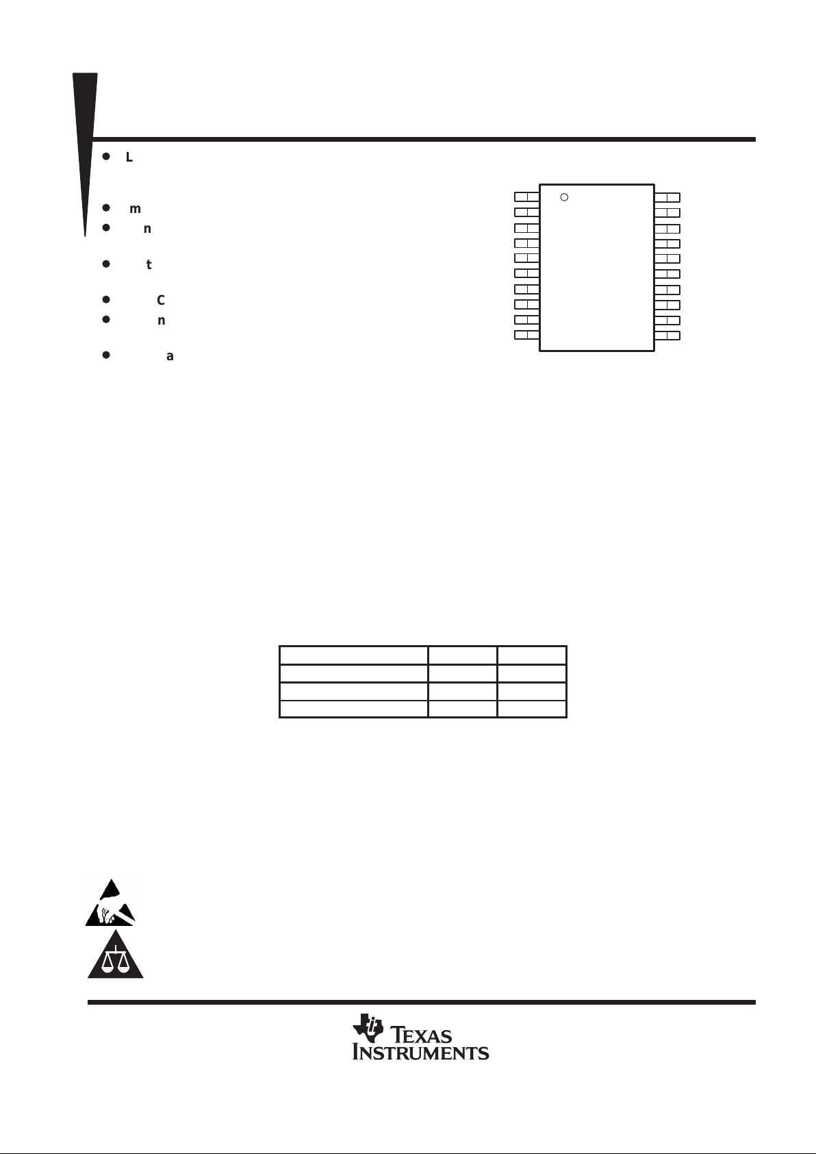
20-Pin Plastic Shrink Small Outline (SSOP)
Package
D
Application-Selectable Internal or External
Oscillator
description
The Texas Instruments (TI) TRF1015 is a single-chip RF downconverter suitable for 900-MHz receiver
applications. It combines a low-noise amplifier (LNA), a buffered voltage-controlled oscillator (VCO), and an RF
mixer into a 20-pin SSOP package requiring very few external components.
Minimal power consumption can be further reduced by placing the required modules into operate mode and the
remaining modules into standby mode.
Three modes of operation are provided for both the LNA and the mixer: standby, low current, and improved
compression. The improved compression mode is suitable for applications that require full duplex capability.
The improved compression mode is suitable for maintaining receiver sensitivity in the presence of large
interfering signals and provides a low bit-error rate (BER) in digital modulation systems. The three modes of
operation are selectable in accordance with the presence of a high or low signal on PD1 and PD2, as shown
in Table 1.
Table 1. Mode Control
MODE PD1 PD2
Standby L L
Low current H H
Improved compression L H
The LNA has a gain of 13 dB and a noise figure of 2.2 dB. LNA input and output characteristic impedances are
50 Ω. The single balanced RF mixer has a gain of 9 dB with a single-sideband (SSB) noise figure of 10 dB. The
VCO has a typical tuning range of 25 MHz using an external varactor and resonator. The VCO gain and tuning
range can be adjusted to meet the phase-locked loop (PLL) design requirement, with an external shunt and
feedback capacitors in series with the resonator. A buf fered output of the VCO provides phase locking capability
and can be configured for single-ended or differential operation.
The TRF1015 is offered in the 20-pin SSOP (DB) package and is characterized for operation from – 40°C
to 85°C free-air temperature.
These devices have limited built-in ESD protection. The leads should be shorted together or the device placed in conductive foam
during storage or handling to prevent electrostatic damage to the MOS gates.
Please be aware that an important notice concerning availability, standard warranty, and use in critical applications of
Texas Instruments semiconductor products and disclaimers thereto appears at the end of this data sheet.
PRODUCTION DATA information is current as of publication date.
Products conform to specifications per the terms of Texas Instruments
standard warranty. Production processing does not necessarily include
testing of all parameters.
Copyright 1998, Texas Instruments Incorporated
1
2
3
4
5
6
7
8
9
10
20
19
18
17
16
15
14
13
12
11
PD1
PD2
AUX_LO–
AUX_LO+
OSC2
VCO_GND
OSC1
VCO_V
CC
VCO_BYP
LNA_GND
MIX_OUT–
MIX_OUT+
MIX_IN
MIX_GND
LNA_GND
LNA_IN
LNA_V
CC
LNA_OUT
LNA_GND
LNA_GND
DB PACKAGE
(TOP VIEW)
TI is a trademark of Texas Instruments Incorporated.
Page 2
TRF1015
RF DOWNCONVERTER
SLWS021D– JUNE 1996 – REVISED JULY 1998
2
POST OFFICE BOX 655303 • DALLAS, TEXAS 75265
functional block diagram
20
19
18
17
3
4
8
10, 11, 12, 16
13
6
5
7
9
15
MIX_OUT–
MIX_OUT+
MIX_IN
MIX_GND
AUX_LO–
AUX_LO+
VCO_V
CC
LNA_GND
LNA_OUT
VCO_GND
OSC2
VCO_BYP
OSC1
LNA_IN
LNA_V
CC
14
Power Down
Logic
Power-Down Signal
To On-Board Circuits
Buffer
Amp
Buffer
Amp
1
2
PD1
PD2
Page 3

TRF1015
RF DOWNCONVERTER
SLWS021D– JUNE 1996 – REVISED JULY 1998
3
POST OFFICE BOX 655303 • DALLAS, TEXAS 75265
Terminal Functions
TERMINAL
NAME NO.
I/O
DESCRIPTION
AUX_LO– 3 O PLL auxiliary local oscillator (LO) output (inverting). AUX_LO – is the inverted output from the auxiliary local
oscillator.
AUX_LO+ 4 O PLL auxiliary LO output (noninverting). AUX_LO+ is the noninverted output from the auxiliary local oscillator.
LNA_GND 10 LNA ground
LNA_GND 11 LNA ground
LNA_GND 12 LNA ground
LNA_GND 16 LNA ground
LNA_IN 15 I LNA RF input. LNA_IN is the RF input signal to the LNA.
LNA_OUT 13 O LNA RF output. LNA_OUT is the RF output from the LNA.
LNA_V
CC
14 LNA voltage supply. The power supply voltage required to operate the LNA is connected to LNA_VCC. See
Application Information section.
MIX_GND 17 Mixer ground
MIX_IN 18 I Mixer RF input. MIX_IN is the RF input to the mixer.
MIX_OUT– 20 O Mixer IF output (inverting). MIX_OUT– is the inverted intermediate frequency (IF) output from the mixer.
MIX_OUT+ 19 O Mixer IF output (noninverting). MIX_OUT+ is the noninverted intermediate frequency (IF) output from the mixer.
OSC1 7 VCO tank port. A coaxial resonator and other tuning components are connected to OSC1 to form the local oscillator
(see Application Information section).
OSC2 5 External oscillator input. An external oscillator can be connected to OSC2. See Application Information section.
PD1 1 I Power down 1 LSB. PD1, along with PD2, determines which sections of the TRF1015 are placed in standby or
operate mode.
PD2 2 I Power down 2 MSB. PD2, along with PD1, determines which sections of the TRF1015 are placed in standby or
operate mode.
VCO_BYP 9 VCO bypass port. An external capacitor can be connected to VCO_BYP when the TRF1015 is configured for local
oscillator operation.
VCO_GND 6 VCO ground
VCO_V
CC
8 VCO voltage supply. The power supply voltage required to operate the VCO is connected to VCO_VCC (see
Application Information section).
absolute maximum ratings over operating free-air temperature range (unless otherwise noted)
Supply voltage range, VCC –0.3 V to 6 V. . . . . . . . . . . . . . . . . . . . . . . . . . . . . . . . . . . . . . . . . . . . . . . . . . . . . . . . . .
Input voltage range, V
I
–0.3 V to VCC + 0.3 V. . . . . . . . . . . . . . . . . . . . . . . . . . . . . . . . . . . . . . . . . . . . . . . . . . . . . .
Power dissipation at or below T
A
= 25°C 200 mW. . . . . . . . . . . . . . . . . . . . . . . . . . . . . . . . . . . . . . . . . . . . . . . . . . .
Operating virtual-junction temperature, T
J
150°C. . . . . . . . . . . . . . . . . . . . . . . . . . . . . . . . . . . . . . . . . . . . . . . . . . .
Operating free-air temperature range, T
A
–40°C to 85°C. . . . . . . . . . . . . . . . . . . . . . . . . . . . . . . . . . . . . . . . . . . .
Storage temperature range, T
stg
–65°C to 125°C. . . . . . . . . . . . . . . . . . . . . . . . . . . . . . . . . . . . . . . . . . . . . . . . . . .
recommended operating conditions
MIN NOM MAX UNIT
Supply voltage, V
CC
3.5 3.75 5.5 V
High-level input voltage, V
IH
VCC–0.5 V
CC
V
Low-level input voltage, V
IL
–0.3 0.5 V
Operating free-air temperature, T
A
–40 85 °C
Operating virtual-junction temperature, T
J
–30 105 °C
Page 4
TRF1015
RF DOWNCONVERTER
SLWS021D– JUNE 1996 – REVISED JULY 1998
4
POST OFFICE BOX 655303 • DALLAS, TEXAS 75265
electrical characteristics at 881 MHz, TA = 25°C, LO = 926 MHz, VCC = 3.75 V; measured in
recommended application circuit board (see Application Information)
cascade (LNA/SAW†/mixer) (IF = 45 MHz)
PARAMETER TEST CONDITIONS MIN TYP MAX UNIT
Power conversion gain PD1 = L, PD2 = H 18 19 21 dB
SSB noise figure PD1 = L, PD2 = H 4.2 5 dB
Input 1-dB compression point PD1 = L, PD2 = H –26 dBm
Input 3rd-order intercept point, 2f2 – f
1
PD1 = L, PD2 = H –19 –14 dBm
LO feedthrough to RF –45 dBm
†
Surface acoustic wave (SAW)
LNA
PARAMETER TEST CONDITIONS MIN TYP MAX UNIT
RF frequency range 869 894 MHz
PD1 = H, PD2 = H 12
Power gain
PD1 = L, PD2 = H 13
dB
PD1 = H, PD2 = H 2
Noise figure
PD1 = L, PD2 = H 2.2
dB
Reverse isolation PD1 = L, PD2 = H –25 dB
Input return loss ZI = 50 Ω, PD1 = L, PD2 = H –10 dB
Output return loss ZO = 50 Ω, PD1 = L, PD2 = H –12 dB
p
p
PD1 = H, PD2 = H –19
Input 1-dB compression
PD1 = L, PD2 = H –14
dBm
p
p
p
PD1 = H, PD2 = H –12
Input 3rd-order intercept point, 2f
2
–
f
1
PD1 = L, PD2 = H –4
dBm
RF mixer
PARAMETER TEST CONDITIONS MIN TYP MAX UNIT
RF frequency range 869 894 MHz
LO frequency range 914 939 MHz
IF frequency 45 MHz
Power conversion gain PD1 = L, PD2 = H 9 dB
SSB noise figure PD1 = L, PD2 = H 10 dB
RF input impedance 50 Ω
LO input impedance External VCO 50 Ω
RF input return loss OSC1 = ZI = 50 Ω –10 dB
LO input return loss OSC1 = ZI = 50 Ω –6 dB
IF output return loss OSC1 = ZO = 50 Ω PD1 = L, PD2 = H –15 dB
Input 1-dB compression point PD1 = L, PD2 = H –10 dBm
Input 3rd-order intercept point, 2f2 – f
1
PD1 = L, PD2 = H 1 dBm
Page 5
TRF1015
RF DOWNCONVERTER
SLWS021D– JUNE 1996 – REVISED JULY 1998
5
POST OFFICE BOX 655303 • DALLAS, TEXAS 75265
electrical characteristics at 881 MHz, TA = 25°C, LO = 926 MHz, VCC = 3.75 V; measured in
recommended application circuit board (see Application Information) (continued)
VCO
PARAMETER TEST CONDITIONS MIN TYP MAX UNIT
Auxiliary LO output power RL = 50 Ω –11 dBm
Phase noise Offset = 60 kHz –114 dBc/Hz
Harmonics –20 dBc
standby mode requirements over recommended operating free-air temperature range and
V
CC
= 3.75 V; (PD1 = L, PD2 = L)
MIN TYP MAX UNIT
LNA 28 100 µA
RF mixer and buffer amplifier 100 µA
VCO 100 µA
low current mode requirements over recommended operating free-air temperature range and
V
CC
= 3.75 V; (PD1 = H, PD2 = H)
MIN TYP MAX UNIT
LNA 2 3 mA
RF mixer and buffer amplifier 14 17 mA
VCO 4 5 mA
improved compression mode requirements over recommended operating free-air temperature
range and V
CC
= 3.75 V; (PD1 = L, PD2 = H)
MIN TYP MAX UNIT
LNA 5 7 mA
RF mixer and buffer amplifier 15 19 mA
VCO 3.75 4.5 mA
Page 6
TRF1015
RF DOWNCONVERTER
SLWS021D– JUNE 1996 – REVISED JULY 1998
6
POST OFFICE BOX 655303 • DALLAS, TEXAS 75265
APPLICATION INFORMATION
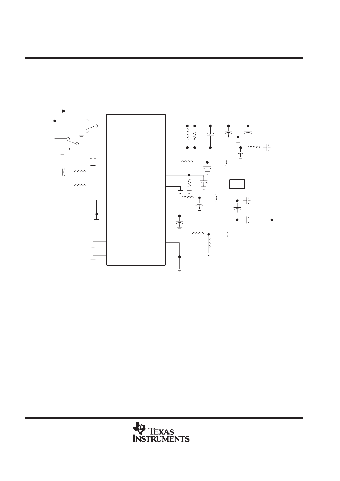
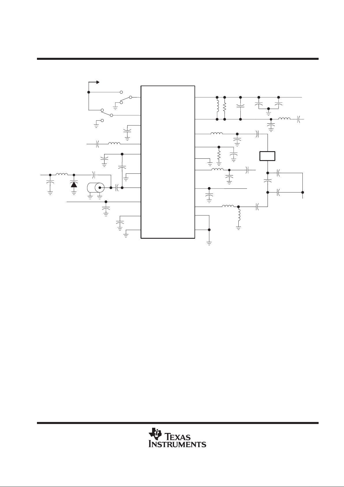
Figure 1 shows the TRF1015 configured using an external oscillator. Figure 2 shows the TRF1015 configured for an
internal oscillator. Table 2 contains a list of the component part numbers and electrical values for the components
shown in Figure 1 and Figure 2. Figure 3 through Figure 6 illustrate the typical performance for mode control when
PD1 = L and PD2 = H.
L4
C12
R1
C11
V
CC
20
19
C21
18
R2
C14
L5
L3
U2
C15
J19
L6
1
17
16
15
14
13
12
11
2
3
4
5
6
7
8
9
10
PD1
PD2
AUX_LO–
AUX_LO+
OSC2
VCO_GND
OSC1
VCO_V
CC
VCO_BYP
LNA_GND
MIX_OUT–
MIX_OUT+
MIX_IN
MIX_GND
LNA_GND
LNA_IN
LNA_V
CC
LNA_OUT
LNA_GND
LNA_GND
C10
C17
C16
C13
L8
C24
C20
V
CC
J15
C18
C23
Optional
C22
Optional
J13
2
3
1
2
3
1
V
CC
C2
C1
L1
L2
J4
J5
C19
L7
Figure 1. Recommended Application Circuit With External Oscillator
Page 7
TRF1015
RF DOWNCONVERTER
SLWS021D– JUNE 1996 – REVISED JULY 1998
7
POST OFFICE BOX 655303 • DALLAS, TEXAS 75265
APPLICATION INFORMATION
L4
C12
R1
C11
V
CC
20
19
C21
18
R2
C14
L5
L3
U2
C15
J19
L6
1
17
16
15
14
13
12
11
2
3
4
PD1
PD2
AUX_LO–
AUX_LO+
MIX_OUT–
MIX_OUT+
MIX_IN
MIX_GND
LNA_GND
LNA_IN
LNA_V
CC
LNA_OUT
LNA_GND
LNA_GND
C10
C17
C16
C13
L8
C24
C20
V
CC
J15
C18
C23
Optional
C22
Optional
J13
2
3
1
2
3
1
V
CC
C2
C1
L1
J4
C19
5
6
7
8
9
10
OSC2
VCO_GND
OSC1
VCO_V
CC
VCO_BYP
LNA_GND
C5
V1
C6
L2
C9
C7
Vdc
C8
P1
C4
vco
Tune
C3
L7
Figure 2. Recommended Application Circuit With Internal Oscillator
Page 8

TRF1015
RF DOWNCONVERTER
SLWS021D– JUNE 1996 – REVISED JULY 1998
8
POST OFFICE BOX 655303 • DALLAS, TEXAS 75265
APPLICATION INFORMATION
Table 2. TRF1015 External Components List
DESIGNATORS DESCRIPTION VALUE MANUFACTURER MANUFACTURER P/N
C1 Capacitor 22 pF Murata GRM36VOG220C50
C2 Capacitor 10 pF Murata GRM36VOG100C50
C3 Capacitor 1 pF Murata GRM36VOG010C50
C4 Capacitor 1 pF Murata GRM36VOG010C50
C5 Capacitor 0.5 pF Murata GRM36VOG05RC50
C6 Capacitor 1.5 pF Venkel Corp CO42COG001ZINB
C7 Capacitor 100 pF Murata GRM36VOG101C50
C8 Capacitor 100 pF Murata GRM36VOG101C50
C9 Capacitor 68 pF Murata GRM36VOG680C50
C10 Capacitor 1000 pF Murata GRM36VOG102C50
C11 Capacitor 100 pF Murata GRM36VOG101C50
C12 Capacitor 56 pF Murata GRM36VOG560C50
C13 Capacitor 18 pF Murata GRM36VOG180C50
C14 Capacitor 12 pF Murata GRM36VOG120C50
C15 Capacitor 100 pF Murata GRM36VOG101C50
C16 Capacitor 22 pF Murata GRM36VOG220C50
C17 Capacitor 3 pF Murata GRM36VOG030C50
C18 Capacitor 22 pF Murata GRM36VOG220C50
C19 Capacitor 100 pF Murata GRM36VOG101C50
C20 Capacitor 22 pF Murata GRM36VOG220C50
C21 Capacitor 68 pF Murata GRM36VOG680C50
C22
†
Capacitor 100 pF Murata GRM36VOG101C50
C23
‡
Capacitor 100 pF Murata GRM36VOG101C50
C24 Capacitor 1 pF Murata GRM36VOG010C50
L1 Coil 10 nH Toko LL1608-F10NJ
L2 Coil 10 nH Toko LL1608-F10NJ
L3 Coil 12 nH Toko LL1608-F12NJ
L4 Coil 220 nH Coilcraft 0805HS-221
L5 Coil 12 nH Toko LL1608-F12NJ
L6 Coil 12 nH Toko LL1608-F12NJ
L7 N/A N/A N/A N/A
L8 Coil 680 nH Murata LQH3NR68M04M00
R1 Resistor 1.5 kΩ Panasonic ERJ-2GEJ152
R2 Resistor 22 Ω Pansonic ERJ-2GEJ220
P1 Coaxial resonator Trans-T ech SR8800LPQ1050BY
U2
Surface acoustic wave
(SAW) bandpass filter
Murata SAEC881-5MA70N
V1 Varactor diode Siemens BBY5L-03W
†
Remove C19 and populate C22 to test the LNA.
‡
Remove C19 and populate C23 to test the mixer.
Page 9

TRF1015
RF DOWNCONVERTER
SLWS021D– JUNE 1996 – REVISED JULY 1998
9
POST OFFICE BOX 655303 • DALLAS, TEXAS 75265
TYPICAL CHARACTERISTICS
Figure 3
T – Temperature – ° C
VCC = 3.75 V
RFIN = –40 dBm @ 881.5 MHz
18
16
14
12
–40 25
G – Cascade Power Conversion Gain – dB
20
22
CASCADE POWER CONVERSION GAIN
vs
TEMPERATURE
24
85
IF = 45 MHz
PD1 = L
PD2 = H
Figure 4
4
3
2
–40 25
Cascade SSB Noise Figure – dB
5
6
CASCADE SSB NOISE FIGURE
vs
TEMPERATURE
7
85
T – Temperature – ° C
VCC = 3.75 V
FREQUENCY = 881.5 MHz
IF = 45 MHz
PD1 = L
PD2 = H
Figure 5
–16
–18
–20
–40 25
IP3 – Input Third Order Intercept Point – dBm
–14
–12
INPUT THIRD ORDER INTERCEPT POINT
vs
TEMPERATURE
–10
85
T – Temperature – ° C
VCC = 3.75 V
FREQUENCY = 881.5 MHz
PD1 = L
PD2 = H
Figure 6
T – Temperature – ° C
2
1
0
–40 25
VCO Tuning Voltage – V
3
4
VCO TUNING VOLTAGE
vs
TEMPERATURE
5
85
VCC = 3.75 V
PD1 = L
PD2 = H
939 MHz
926.5 MHz
914 MHz
Page 10

TRF1015
RF DOWNCONVERTER
SLWS021D– JUNE 1996 – REVISED JULY 1998
10
POST OFFICE BOX 655303 • DALLAS, TEXAS 75265
TYPICAL CHARACTERISTICS
20
15
5
0
0.1 1 10 100
Maximum Available Gain – dB
25
30
f – Frequency – MHz
LNA MAXIMUM AVAILABLE GAIN
vs
FREQUENCY
35
1e+03 1e+04
10
PD1 = L
PD2 = H
Figure 7
Table 3. LNA Maximum Available Gain
(PD1 = L, PD2 = H)
FREQUENCY
MHz
GMAX
dB
200.000 27.86
250.000 26.25
300.000 25.56
350.000 24.92
400.000 23.17
450.000 21.57
500.000 20.39
550.000 19.29
600.000 18.36
650.000 17.55
700.000 16.84
750.000 16.22
800.000 15.71
850.000 15.28
900.000 14.88
950.000 14.54
1000.000 14.28
1050.000 13.97
1100.000 13.68
Page 11

TRF1015
RF DOWNCONVERTER
SLWS021D– JUNE 1996 – REVISED JULY 1998
11
POST OFFICE BOX 655303 • DALLAS, TEXAS 75265
TYPICAL CHARACTERISTICS
20
15
5
0
0.1 1 10 100
Maximum Available Gain – dB
25
30
f – Frequency – MHz
35
1e+03 1e+04
10
PD1 = H
PD2 = H
LNA MAXIMUM AVAILABLE GAIN
vs
FREQUENCY
Figure 8
Table 4. LNA Maximum Available Gain
(PD1 = H, PD2 = H)
FREQUENCY
MHz
GMAX
dB
200.000 24.98
250.000 23.97
300.000 23.04
350.000 22.38
400.000 21.64
450.000 21.25
500.000 20.79
550.000 20.30
600.000 19.99
650.000 18.72
700.000 17.52
750.000 16.73
800.000 15.99
850.000 15.33
900.000 14.89
950.000 14.47
1000.000 14.20
1050.000 13.72
1100.000 13.49
Page 12

TRF1015
RF DOWNCONVERTER
SLWS021D– JUNE 1996 – REVISED JULY 1998
12
POST OFFICE BOX 655303 • DALLAS, TEXAS 75265
TYPICAL CHARACTERISTICS
2
0
5210.50.20
0.2
0.5
1
5
–0.2
–0.5
–1
–2
–5
M1
M2
M3
M4
S22
S11
M1 Frequency = 200 MHz
M2 Frequency = 1100 MHz
M3 Frequency = 200 MHz
M4 Frequency = 1100 MHz
LNA S–Parameters (S11, S22); PD1 = H, PD2 = H
Frequency 200 to 1100 MHz
Figure 9 Figure 10
M1
M2
1.22.43.64.66
LNA S–Parameter (S21); PD1 = H, PD2 = H
M1 Frequency = 200 MHz
M2 Frequency = 1100 MHz
Frequency 200 to 1100 MHz
∞
M2
M1
0.0120.0240.0360.0480.06
LNA S–Parameter (S12); PD1 = H, PD2 = H
M1 Frequency = 200 MHz
M2 Frequency = 1100 MHz
Figure 11
Frequency 200 to 1100 MHz
Page 13

TRF1015
RF DOWNCONVERTER
SLWS021D– JUNE 1996 – REVISED JULY 1998
13
POST OFFICE BOX 655303 • DALLAS, TEXAS 75265
TYPICAL CHARACTERISTICS
Table 5. LNA S-Parameters (PD1 = H, PD2 = H)
FREQUENCY
MHz
S11
Mag
S11
Ang/Deg
S21
Mag
S21
Ang/Deg
S12
Mag
S12
Ang/Deg
S22
Mag
S22
Ang/Deg
200.000 0.9161 –25.3740 5.7502 155.0000 0.0183 75.7670 0.7078 –13.7230
250.000 0.8978 –31.1611 5.5760 149.3856 0.0024 70.3898 0.6956 –16.5954
300.000 0.8746 –36.9489 5.3813 144.1056 0.0267 68.0219 0.6818 –19.2064
350.000 0.8505 –42.4277 5.1920 138.8600 0.0300 65.1007 0.6673 –21.9170
400.000 0.8268 –47.6840 5.0138 134.1978 0.0344 62.9150 0.6534 –24.6232
450.000 0.7971 –52.5767 4.8099 129.3022 0.0360 60.6094 0.6366 –27.0642
500.000 0.7710 –57.3827 4.6077 125.0000 0.0384 57.6460 0.6228 –29.5297
550.000 0.7445 –61.7972 4.4172 120.7844 0.0413 56.4048 0.6072 –31.7974
600.000 0.7237 –65.9348 4.2476 117.0256 0.0425 55.9867 0.5934 –33.5836
650.000 0.6990 –70.0200 4.0650 113.2600 0.0435 54.2110 0.5782 –35.9930
700.000 0.6796 –73.8781 3.8898 109.8389 0.0464 52.3697 0.5665 –37.4491
750.000 0.6654 –77.2861 3.7258 106.6278 0.0480 53.5603 0.5548 –39.1324
800.000 0.6505 –80.9020 3.5840 103.7567 0.0490 52.3890 0.5461 –40.7757
850.000 0.6363 –84.4913 3.4536 100.8822 0.0503 51.1741 0.5369 –42.1322
900.000 0.6232 –88.1152 3.3373 98.0539 0.0528 52.6742 0.5284 –43.6353
950.000 0.6115 –91.9600 3.2330 95.5650 0.0539 52.7493 0.5247 –45.0560
1000.000 0.6036 –95.2078 3.1581 93.2986 0.0561 52.4254 0.5793 –46.7002
1050.000 0.5896 –99.2981 3.0540 90.2556 0.0584 51.8791 0.5136 –47.7220
1100.000 0.5808 –102.8000 2.9963 87.9460 0.0601 52.6700 0.5098 –48.9450
Page 14

TRF1015
RF DOWNCONVERTER
SLWS021D– JUNE 1996 – REVISED JULY 1998
14
POST OFFICE BOX 655303 • DALLAS, TEXAS 75265
TYPICAL CHARACTERISTICS
2
0
5210.50.20
0.2
0.5
1
5
∞
–0.2
–0.5
–1
–2
–5
M1
M2
M3
M4
S22
S11
M1 Frequency = 200 MHz
M2 Frequency = 1100 MHz
M3 Frequency = 200 MHz
M4 Frequency = 1100 MHz
LNA S–Parameters (S11, S22); PD1 = L, PD2 = H
Frequency 200 to 1100 MHz
Figure 12
M1
M2
2.24.46.68.811
LNA S–Parameter (S21); PD1 = L, PD2 = H
M1 Frequency = 200 MHz
M2 Frequency = 1100 MHz
Figure 13
Frequency 200 to 1100 MHz
M1
M2
LNA S–Parameter (S12); PD1 = L, PD2 = H
M1 Frequency = 200 MHz
M2 Frequency = 1100 MHz
0.010.020.030.040.05
Figure 14
Frequency 200 to 1100 MHz
0.06
Page 15

TRF1015
RF DOWNCONVERTER
SLWS021D– JUNE 1996 – REVISED JULY 1998
15
POST OFFICE BOX 655303 • DALLAS, TEXAS 75265
TYPICAL CHARACTERISTICS
Table 6. LNA S-Parameters (PD1 = L, PD2 = H)
FREQUENCY
MHz
S11
Mag
S11
Ang/Deg
S21
Mag
S21
Ang/Deg
S12
Mag
S12
Ang/Deg
S22
Mag
S22
Ang/Deg
200.000 0.8184 –37.1670 10.1790 143.9800 0.0167 72.9150 0.6334 –18.5750
250.000 0.7767 –45.0520 9.5611 136.6800 0.0227 66.1208 0.6068 –21.9252
300.000 0.7297 –52.2266 8.9451 129.9789 0.0248 62.2804 0.5838 –24.5579
350.000 0.6862 –58.5890 8.3266 123.9900 0.0268 61.3593 0.5600 –27.0387
400.000 0.6468 –64.2456 7.7678 118.8544 0.0286 58.3873 0.5396 –29.2259
450.000 0.6077 –69.4464 7.2199 113.9089 0.0319 57.1011 0.5189 –31.3796
500.000 0.5784 –74.0750 6.7222 109.5833 0.0335 58.0690 0.5029 –33.4613
550.000 0.5488 –78.5661 6.2707 105.6556 0.0352 57.6446 0.4863 –34.9911
600.000 0.5255 –82.2168 5.8843 102.1911 0.0365 55.5490 0.4744 –36.0988
650.000 0.5066 –85.7060 5.5023 98.9850 0.0372 57.7150 0.4606 –37.9700
700.000 0.4908 –89.3091 5.1689 96.1968 0.0407 56.8278 0.4478 –38.9564
750.000 0.4810 –92.3593 4.8897 93.5827 0.0406 57.3591 0.4404 –40.0151
800.000 0.4733 –95.6787 4.6458 91.2930 0.0429 58.0943 0.4324 –41.3110
850.000 0.4681 –99.0036 4.4381 89.0728 0.0435 59.6353 0.4287 –42.3419
900.000 0.4637 –102.5756 4.2488 86.7164 0.0461 60.9984 0.4228 –43.5259
950.000 0.4580 –106.6767 4.0818 84.7387 0.0499 60.9513 0.4211 –44.7310
1000.000 0.4565 –110.5256 3.9597 82.7031 0.0509 60.4970 0.4198 –45.9854
1050.000 0.4505 –114.3411 3.8157 80.31 11 0.0562 60.9322 0.4152 –46.8147
1100.000 0.4462 –118.1800 3.6975 78.4010 0.0571 61.4270 0.4150 –48.2590
Page 16

2
0
5210.50.20
0.2
0.5
1
5
∞
–0.2
–0.5
–1
–2
–5
M1
M2
M1 Frequency = 200 MHz
M2 Frequency = 1100 MHz
Mixer RF Input (MIX_IN) S–Parameter (S11)
Frequency 200 to 1100 MHz
Figure 15
2
0
5210.50.20
0.2
0.5
1
5
∞
–0.2
–0.5
–1
–2
–5
M1
M2
M1 Frequency = 200 MHz
M2 Frequency = 1100 MHz
Mixer LO Input (OSC2) S–Parameter (S11)
Frequency 200 to 1100 MHz
Figure 16
TRF1015
RF DOWNCONVERTER
SLWS021D– JUNE 1996 – REVISED JULY 1998
16
POST OFFICE BOX 655303 • DALLAS, TEXAS 75265
TYPICAL CHARACTERISTICS
Table 7. Mixer RF Input (MIX_IN) S-Parameter (S11)
FREQUENCY
MHz
S11
Mag
S11
Ang/Deg
200.000 0.8735 –17.8209
250.000 0.8848 –22.7093
300.000 0.8802 –27.3606
350.000 0.8800 –33.2514
400.000 0.8696 –38.4946
450.000 0.8511 –44.2309
500.000 0.8288 –50.4016
550.000 0.7883 –56.4141
600.000 0.7484 –62.1003
650.000 0.6921 –66.5583
700.000 0.6333 –69.8291
750.000 0.5913 –71.9388
800.000 0.5444 –72.4816
850.000 0.5133 –72.4310
900.000 0.4948 –71.8818
950.000 0.4915 –70.6215
1000.000 0.4914 –69.6679
1050.000 0.5013 –69.7537
1100.000 0.5133 –69.6625
Table 8. Mixer LO Input (OSC2) S-Parameter (S11)
FREQUENCY
MHz
S11
Mag
S11
Ang/Deg
200.000 0.8607 –13.8790
250.000 0.8494 –16.7136
300.000 0.8343 –19.4041
350.000 0.8242 –22.1589
400.000 0.8123 –24.8431
450.000 0.8015 –27.4343
500.000 0.7917 –30.0491
550.000 0.7805 –32.5775
600.000 0.7701 –35.0397
650.000 0.7591 –37.6443
700.000 0.7504 –40.1119
750.000 0.7402 –42.4656
800.000 0.7297 –45.1661
850.000 0.7191 –47.5184
900.000 0.7074 –49.9772
950.000 0.6965 –52.2767
1000.000 0.6832 –54.8612
1050.000 0.6741 –56.9238
1100.000 0.6606 –59.3890
Page 17

M1
M2
2
0
5210.50.20
0.2
0.5
1
5
∞
–0.2
–0.5
–1
–2
–5
M1 Frequency = 200 MHz
M2 Frequency = 1100 MHz
Frequency 200 to 1100 MHz
Mixer IF Output (MIX_OUT–, MIX_OUT+) Differential
1-Port S-Parameter (S11)
Figure 17
TRF1015
RF DOWNCONVERTER
SLWS021D– JUNE 1996 – REVISED JULY 1998
17
POST OFFICE BOX 655303 • DALLAS, TEXAS 75265
TYPICAL CHARACTERISTICS
Table 9. Mixer IF Output (MIX_OUT–, MIX_OUT+)
Differential 1-Port S-Parameter (S11)
FREQUENCY
MHz
S11
Mag
S11
Ang/Deg
200.000 0.9779 –3.6814
250.000 0.9608 –8.7853
300.000 0.9610 –12.4887
350.000 0.9606 –15.1696
400.000 0.9396 –17.8656
450.000 0.9225 –19.9763
500.000 0.9195 –22.4088
550.000 0.9101 –24.5839
600.000 0.9037 –26.2246
650.000 0.8929 –28.0952
700.000 0.8808 –29.8886
750.000 0.8825 –30.3742
800.000 0.8498 –32.8607
850.000 0.8296 –33.9195
900.000 0.8034 –34.7265
950.000 0.7947 –34.7224
1000.000 0.7837 –35.2351
1050.000 0.7732 –35.4152
1100.000 0.7645 –35.6687
Page 18

TRF1015
RF DOWNCONVERTER
SLWS021D– JUNE 1996 – REVISED JULY 1998
18
POST OFFICE BOX 655303 • DALLAS, TEXAS 75265
TYPICAL CHARACTERISTICS
2
0
5210.50.20
0.2
0.5
1
5
∞
–0.2
–0.5
–1
–2
–5
M1
M2
M3
M4
OSC2
M1 Frequency = 200 MHz
M2 Frequency = 1100 MHz
M3 Frequency = 200 MHz
M4 Frequency = 1100 MHz
OSC1 and OSC2 S–Parameters (S11)
Frequency 200 to 1100 MHz
OSC1
Figure 18
T able 10. OSC1 and OSC2 S-Parameters (S11)
OSC1 OSC2
FREQUENCY
MHz
S11
Mag
S11
Ang/Deg
S11
Mag
S11
Ang/Deg
200.000 1.0001 –11.1803 0.7619 –18.2426
250.000 1.0091 –14.1781 0.7490 –22.3585
300.000 1.0186 –17.1156 0.7335 –26.1657
350.000 1.0318 –20.3634 0.7222 –30.0057
400.000 1.0466 –23.8789 0.7086 –33.7792
450.000 1.0645 –27.5708 0.6952 –37.5559
500.000 1.0880 –31.8085 0.6852 –41.2834
550.000 1.1065 –36.5770 0.6663 –45.3924
600.000 1.1245 –42.2143 0.6533 –47.4515
650.000 1.1390 –48.8065 0.6464 –51.3596
700.000 1.1247 –56.1964 0.6357 –54.8598
750.000 1.0790 –64.0879 0.6250 –58.3133
800.000 0.9931 –71.3472 0.6122 –61.6874
850.000 0.8886 –76.6167 0.6022 –65.1014
900.000 0.7913 –78.8757 0.5919 –68.1511
950.000 0.7180 –79.4862 0.5820 –71.2731
1000.000 0.6717 –78.4849 0.5735 –74.3303
1050.000 0.6468 –77.7310 0.5634 –77.2926
1100.000 0.6362 –76.7557 0.5556 –80.1574
Page 19

M1
M2
2
0
5210.50.20
0.2
0.5
1
5
∞
–0.2
–0.5
–1
–2
–5
M1 Frequency = 200 MHz
M2 Frequency = 1100 MHz
Frequency 200 to 1100 MHz
Buffer Amplifier (AUX_LO, AUX_LO+) Differential
1–Port S–Parameter (S11)
Figure 19
TRF1015
RF DOWNCONVERTER
SLWS021D– JUNE 1996 – REVISED JULY 1998
19
POST OFFICE BOX 655303 • DALLAS, TEXAS 75265
TYPICAL CHARACTERISTICS
T able 11. Buffer Amplifier (AUX_LO–, AUX_LO+)
Differential 1-Port S-Parameter (S11)
FREQUENCY
MHz
S11
Mag
S11
Ang/Deg
200.000 0.9113 –4.6025
250.000 0.9116 –5.6696
300.000 0.9096 –6.9046
350.000 0.9074 –8.0997
400.000 0.9068 –9.2593
450.000 0.9042 –10.3757
500.000 0.9037 –11.6629
550.000 0.9010 –12.9567
600.000 0.8994 –14.1240
650.000 0.8969 –15.4441
700.000 0.8951 –16.6305
750.000 0.8935 –18.0071
800.000 0.8890 –19.1919
850.000 0.8868 –20.4675
900.000 0.8834 –21.7876
950.000 0.8809 –22.9685
1000.000 0.8769 –24.2356
1050.000 0.8740 –25.4904
1100.000 0.8706 –26.6875
Page 20

TRF1015
RF DOWNCONVERTER
SLWS021D– JUNE 1996 – REVISED JULY 1998
20
POST OFFICE BOX 655303 • DALLAS, TEXAS 75265
MECHANICAL DATA
DB (R-PDSO-G**) PLASTIC SMALL-OUTLINE PACKAGE
4040065 /D 02/98
28 PIN SHOWN
Gage Plane
8,20
7,40
0,15 NOM
0,63
1,03
0,25
38
12,90
12,30
28
10,50
24
8,50
Seating Plane
9,907,90
30
10,50
9,90
0,38
5,60
5,00
15
0,22
14
A
28
1
2016
6,50
6,50
14
0,05 MIN
5,905,90
DIM
A MAX
A MIN
PINS **
2,00 MAX
6,90
7,50
0,65
M
0,15
0°–8°
0,10
NOTES: A. All linear dimensions are in millimeters.
B. This drawing is subject to change without notice.
C. Body dimensions do not include mold flash or protrusion not to exceed 0,15.
D. Falls within JEDEC MO-150
Page 21

IMPORTANT NOTICE
T exas Instruments and its subsidiaries (TI) reserve the right to make changes to their products or to discontinue
any product or service without notice, and advise customers to obtain the latest version of relevant information
to verify, before placing orders, that information being relied on is current and complete. All products are sold
subject to the terms and conditions of sale supplied at the time of order acknowledgement, including those
pertaining to warranty, patent infringement, and limitation of liability.
TI warrants performance of its semiconductor products to the specifications applicable at the time of sale in
accordance with TI’s standard warranty. Testing and other quality control techniques are utilized to the extent
TI deems necessary to support this warranty. Specific testing of all parameters of each device is not necessarily
performed, except those mandated by government requirements.
CERT AIN APPLICATIONS USING SEMICONDUCTOR PRODUCTS MAY INVOLVE POTENTIAL RISKS OF
DEATH, PERSONAL INJURY, OR SEVERE PROPERTY OR ENVIRONMENTAL DAMAGE (“CRITICAL
APPLICATIONS”). TI SEMICONDUCTOR PRODUCTS ARE NOT DESIGNED, AUTHORIZED, OR
WARRANTED TO BE SUITABLE FOR USE IN LIFE-SUPPORT DEVICES OR SYSTEMS OR OTHER
CRITICAL APPLICATIONS. INCLUSION OF TI PRODUCTS IN SUCH APPLICA TIONS IS UNDERST OOD TO
BE FULLY AT THE CUSTOMER’S RISK.
In order to minimize risks associated with the customer’s applications, adequate design and operating
safeguards must be provided by the customer to minimize inherent or procedural hazards.
TI assumes no liability for applications assistance or customer product design. TI does not warrant or represent
that any license, either express or implied, is granted under any patent right, copyright, mask work right, or other
intellectual property right of TI covering or relating to any combination, machine, or process in which such
semiconductor products or services might be or are used. TI’s publication of information regarding any third
party’s products or services does not constitute TI’s approval, warranty or endorsement thereof.
Copyright 1998, Texas Instruments Incorporated
 Loading...