

Page 1

TRAC® SUPPORT CIRCUIT
ISSUE 1 - JANUARY 2000
DEVICE DESCRIPTION
The TRAC family of Field Programmable
Analog Devices offers an integrated path from
signal processing problems to working silicon
solutions - in minutes! The Totally
Reconfigurable Analog Circuit is a highly
flexible single chip solution to the signal
processing problems found in many markets.
Introducing a Top-Down, Structured design
discipline, TRAC enables rapid
implementation, prototyping and product
release. Rather than working at the component
level, TRAC champions the Computational
Approach, providing designers with benefits
formerly associated only with programmable
digital devices. TRAC brings a truly integrated
Signal Processing problem solving process,
offering a path to Custom Silicon for higher
volume users.
TRAC devices have to be loaded with program
data at power-up and run from a split 5V
supply. By integrating the loading interface
circuitry, voltage regulation, supply
monitoring and thermal protection, the TRAC
support circuit (TRAC-S2) further simplifies
circuit integration and interface with memory
devices.
An adjustable frequency oscillator clocks
program data out of a serial output memory
device and into any number of cascaded TRAC
devices. By monitoring the bit stream pattern,
TRAC-S2 can sense when loading is complete
and stop clocking automatically.
An adjustable ‘rail-splitter’ generates the
ground supply rail, and the supply monitoring
function initiates program load on power-up,
and after power failure or serious fluctuation.
Thermal shutdown further protects the device
against overheating.
TRAC-S2
FEATURES & BENEFITS
Makes designing TRAC circuits easier,
production prototyping quicker
Reduces component count and
manufacturing costs
Enables simple connection of a serial output
EEPROM or other memory device to TRAC
Compatible with current and future TRAC
devices
Automatic program loading at power-up
Supply monitor function reloads program
after power failure or fluctuation
Frequency of on-chip oscillator user-defined
Senses number of cascaded TRAC devices
automatically
Automatically stops clocking when program
loading complete
Simplifies generation of TRAC supply
voltages
Ground voltage user defined
Thermal shutdown function protects against
overloading due to circuit failures
Full industrial temperature range
ORDERING INFORMATION
PART NUMBER PACKAGE PART
TRAC-S2Q16 QSOP16 TRAC-S2
MARK
1
Page 2
TRAC-S2
ABSOLUTE MAXIMUM RATINGS
Supply Voltage 0V to +7V
Supply Current 50mA
Operating Temperature Range -40°C to 85°C
Storage Temperature Range -55°C to 125°C
ELECTRICAL CHARACTERISTICS
Test Conditions: Temperature=25°C, V
100nF between AGND_OUT and V
PARAMETER CONDITIONS MIN TYPICAL MAX
Supply Voltage Operating Range 4.8V 5.0V 5.2V
Supply Current Standby (CLCR_IN = 0V)
RAIL SPLITTER
SETV(Input Current) SETV = 2.50V 50nA 200nA
AGND_OUT
(Output Voltage)
AGND_OUT
(Output Voltage)
SUPPLY MONITOR
RESET_OUT
(Threshold Voltage)
RESET_OUT (Hysteresis) 0.01V 0.02V 0.08V
RESET_OUT
(Onstate output sink current)
RESET_OUT
(Offstate output current)
PROPAGATION DELAY VDD step from 5.0V to 4.0V
PROGRAMMING LOGIC
CLK_OUT
(Frequency)
CLK_OUT
(Max Programming Frequency)
CLK_OUT
(High output voltage)
NOT CLK_OUT(Frequency) 2.2nF between CAP and V
NOT CLK_OUT(High output
voltage)
Clocking (CLCR_IN = 5V)
SETV = 2.50V (No Load)
SETV = 2.0V (No Load)
SETV = 2.50V; I
SETV = 2.50V; I
High State Output (VDD increasing)
Low State Output (VDD decreasing)
VDD = RESET_OUT = 4V 0.14mA
VDD = RESET_OUT = 5V 0.18mA
2.2nF between CAP and V
CLCR_IN = 5V
47pF between CAP and V
CLCR_IN = 5V
2.2nF between CAP and V
CLCR_IN = 5V
CLCR_IN = 5V
2.2nF between CAP and V
CLCR_IN = 5V
=5V, VSS=0V, CLCR_IN=0V,
DD
, unless otherwise stated.
SS
1.5mA
2.9mA
2.49V
1.99V
= 20mA
SINK
= 2 0 mA AGND_OUT
SOURCE
SS
SS
SS
SS
SS
- 0.010V
4.35V
4.35V
7kHz 10kHz 15kHz
3.90V 4.10V 4.50V
7kHz 10kHz 15kHz
4.00V 4.20V 4.60V
1.9mA
3.7mA
2.50V
2.00V
4.67V
4.65V
S
1
2.8mA
5.5mA
2.51V
2.01V
AGND_OUT
+ 0.010V
4.75V
4.75V
200kHz
2
Page 3
TRAC-S2
ELECTRICAL CHARACTERISTICS
Test Conditions: Temperature=25°C, V
100nF between AGND_OUT and V
DATA_OUT(Frequency) 2.2nF between CAP and V
DATA_OUT(High output
voltage)
SELECT
(Output Voltage)
CLCR_IN = 5V
2.2nF between CAP and V
CLCR_IN = 5V
2.2nF between CAP and V
CLCR_IN = 5V
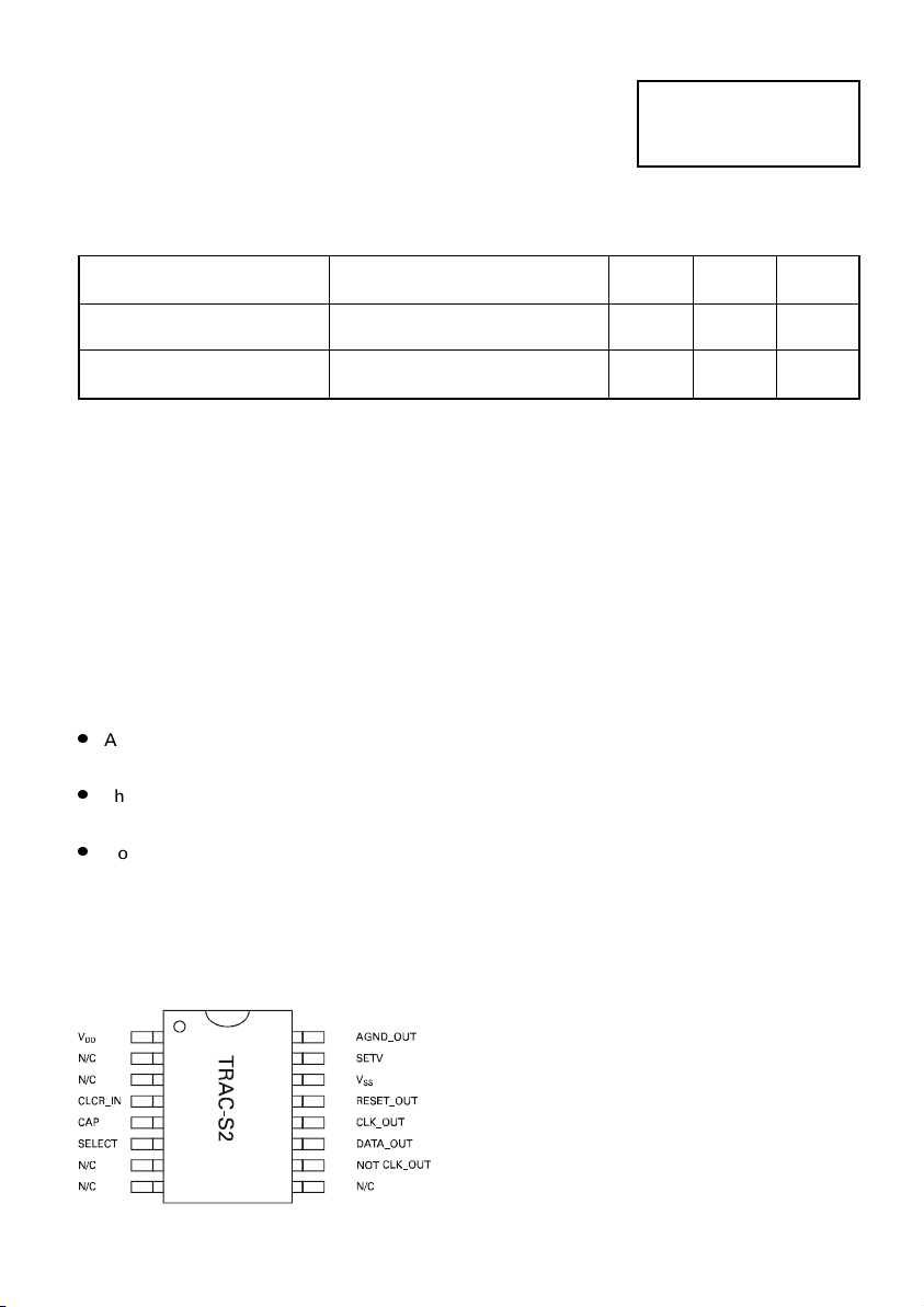
DESCRIPTION OF PIN FUNCTIONS
Inputs
SETV Defines the AGND_OUT voltage. Normally set by potential divider
CLCR_IN Active high to enable clock
CAP Capacitor to V
Outputs
AGND_OUT Analog Ground. Able to source and sink current
SELECT Active high when CLCR_IN is logic high. Enables memory device
CLK_OUT Fed to EEPROM clock input
NOT CLK_OUT Fed to TRAC clock input
DATA_OUT CLK_OUT divided by four. Fed to serial output memory device
RESET_OUT Reset for TRAC Support Circuit and TRAC devices
sets clock frequency
SS
General notes for the TRAC Support Circuit
An on-chip oscillator produces the output CLK_OUT and NOT CLK_OUT. CLCR_IN must be logic high
(V
) to activate CLK_OUT and NOT CLK_OUT
DD
The CLK_OUT output frequency is divided by four to give the DATA_OUT output. Therefore CLCR_IN
must be logic high (V
For AGND_OUT stability under load, a 100nF capacitor is required between AGND_OUT and V
) to activate DATA_OUT
DD
=5V, VSS=0V, CLCR_IN=0V,
DD
, unless otherwise stated.
SS
SS
SS
SS
1.7kHz 2.5kHz 4.0kHz
3.90V 4.10V 4.50V
4.8V 4.99V 5.00V
SS
3
Page 4

TRAC-S2
4
Page 5

TRAC-S2
5
Page 6

TRAC-S2
BLOCK DIAGRAM
Description of the TRAC Support Circuit
1) Rail Splitter
This section provides the analog ground rail between the 5V supply. An external potential divider
can be connected to the SETV pin which enables AGND_OUT to be set to the desired potential. The
output stage of the rail splitter has been designed to provide power capabilities for 4 TRAC devices
and accompanying circuitry. The circuit has low output resistance enabling a drive capability of +/20mA.
2) Supply Monitor
This section utilises the precision ZSM560 supply monitor design. The RESET_OUT provides a signal
to reset all the devices included in the programming and operation of TRAC . This ensures that all
devices are switched on and off simultaneously.
3) Programming Logic
This section provides TRAC and memory with the signals required for programming. The clock is
generated on chip, with the frequency set by an exte rnal capacitor. The DATA_OUT signal is generated
by dividing the clock frequency by 4. This provides the code to initialise an EEPROM and prompt it to
output data. The SELECT pin enables EEPROM chip select.
This section also takes an input signal from the final TRAC device, CLCR_IN. This signal is normally
‘high’ and goes ‘low’ when programming is complete, and is used to terminate the CLK_OUT and
DATA_OUT signals.
6
Page 7

TRAC-S2
APPLICATION CIRCUIT
Connections between the support circuit, the EEPROM and the TRAC device are shown above.
For a more detailed explanation of the circuit see the application note AN27, “How to use the TRAC
support chip”. This also shows the circuit required to program multiple TRAC devices.
LIST OF COMPATIBLE MEMORY DEVICES
ST9346CB1 (SGS-Thomson)
93LC46B (Microchip)
NM92C46 (National Semiconductor)
7
Page 8

TRAC-S2
PACKAGE DIMENSIONS
IDENTIFICATION
RECESS
FOR PIN 1
A
B
C
J
PIN No.1
F
G
QSOP16
PIN Millimetres Inches
MIN MAX MIN MAX
A 4.80 4.98 0.189 0.196
B 0.635 0.025 NOM
C 0.177 0.267 0.007 0.011
D 0.20 0.30 0.008 0.012
E 3.81 3.99 0.15 0.157
F 1.35 1.75 0.053 0.069
G 0.10 0.25 0.004 0.01
J 5.79 6.20 0.228 0.244
K0° 8° 0° 8°
E
D
K
Zetex plc.
Fields New Road, Chadderton, Oldham, OL9-8NP, United Kingdom.
Telephone: (44)161 622 4422 (Sales), (44)161 622 4444 (General Enquiries)
Fax: (44)161 622 44 20
Zetex GmbH Zetex Inc. Zetex (Asia) Ltd. These are supported by
Streitfeldstraße 19 47 Mall Drive, Unit 4 3510 Metroplaza, Tower 2 agents and distributors in
D-81673 München Commack NY 11725 Hing Fo ng Road, major countries wor ld-wide
Germany USA Kwai Fong, Hong Kong
Telefon: (49) 89 45 49 49 0 Telephone: (63 1) 543-7100 T elephone:(852 ) 26100 611
Fax: (49) 89 45 49 49 49 Fax: (631) 864-7630 Fax: (852) 24250 494 Internet:http://www.zetex.com
This publication is issued to provide outline information only which (unless agreed by the Company in writing) may not be used, applied
or reproduced for any purpose or form part of any order or contract or be regarded as a representation relating to the products or
services concerned. The Company reserves the right to alter without notice the specification, design, price or conditions of supply of
any product or service.
Zetex plc 2000
8
 Loading...