

Page 1

TOTALLY RE-CONFIGURABLE ANALOG
CIRCUIT - TRAC
Issue 2 - MARCH 1999
®
TRAC020LH
DEVICE DESCRIPTION
The TRAC020LH is a Micro-Power version of
the existing TRAC products. It also offers
significant improvements in bandwidth and
function accuracy.
The TRAC020LH is the latest addition to the
TRAC family of Field Programmable Analog
Devices (FPAD ) which offers an integrated path
from signal processing problems to working
silicon solutions - in minutes! The Totally
Reconfigurable Analog Circuit is a highly
flexible single chip solution to the signal
processing problems found in many markets.
Introducing a Top-Down, Structured design
discipline, TRAC enables rapid
implementation, prototyping and product
release. Rather than working at the component
level, TRAC champions the Computational
Approach, providing designers with benefits
formerly associated with programmable
digital devices. TRAC brings a truly integrated
Signal Processing problem solving process
and offers a path to Custom Silicon for high
volume applications.
APPLICATIONS
Many analog signal processing applications
including:-
• Analog Computation
• Analog Signal Processing (ASP)
• Classical & Modern Control Systems
• Audio Applications
• Sonar and Ultrasonic Systems
• Analog Correlation
• Echo Cancellation
• Log, Linear and Modern Filter Design
• Instrumentation
• Transducer Characteristic Correction
• Vector Analysis
FEATURES AND BENEFITS
• Faster design and verification of signal
processing solutions
• Instant working silicon
• Flexibility to react to changing requirements
• Stay thinking about analog problems
mathematically - minimal circuit design
• Just as versatile as FPGA - and just as easy
• Complete more projects on time
• High level of integration and design secrecy
• Integration with other CAE systems
• Transparent design migration to
semi-custom and future devices
• Less than 8 bytes to program
• Full industrial temperature range
• Standby mode for improved battery life
• Devices easily cascaded for more complex
designs
• Combines silicon, software and support
ORDERING INFORMATION
PART NUMBER PACKAGE PART
MARK
TRAC020LHQ36 QSOP36 TRAC020LH
For more information on Fast Analog Solutions and all our products see www.fas.co.uk
1
Page 2
TRAC020LH
ABSOLUTE MAXIMUM RATINGS
Voltage on any pin = 7.0V (relative to VSS)
Operating Temperature = -40 to 85°C
Storage Temperature = -55 to 125°C
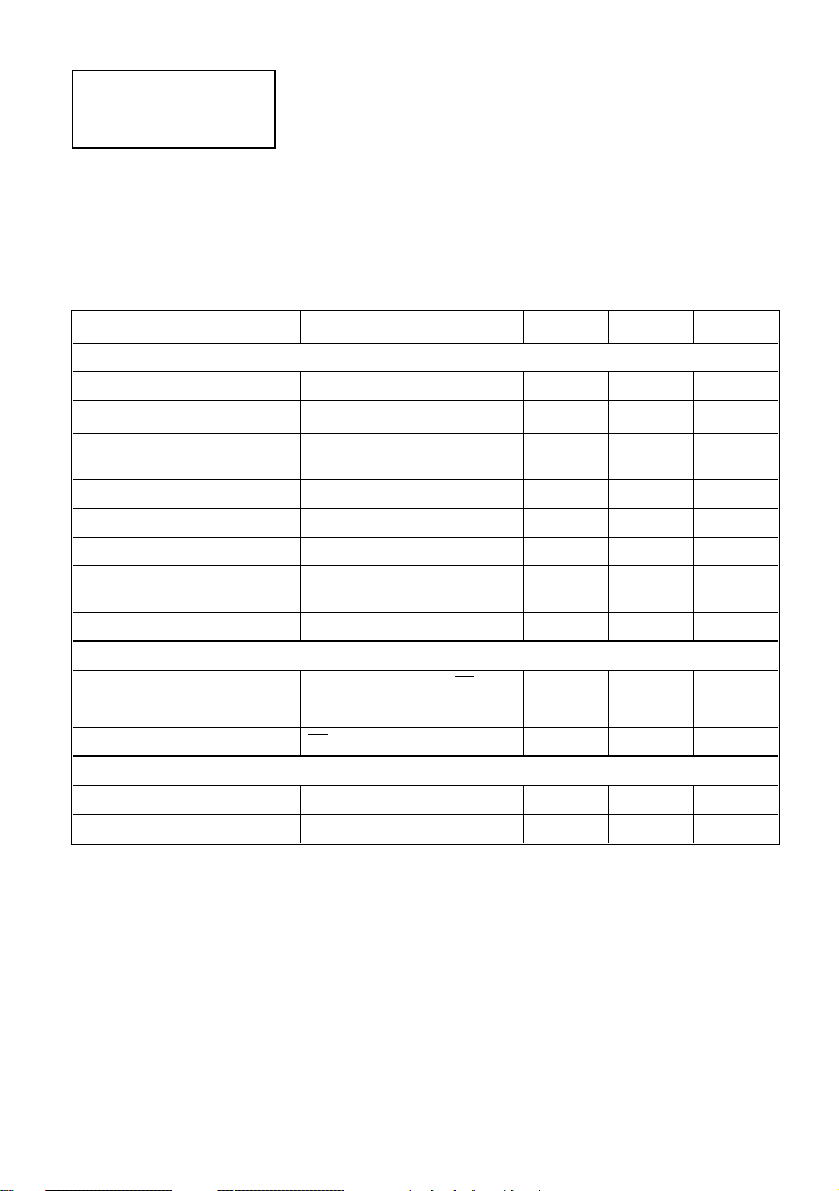
GENERAL ELECTRICAL CHARACTERISTICS
Test Conditions: Temperature = 25 °C, VDD = 3.0V±0.15V, VSS = -2.0V±0.10V
PARAMETER CONDITIONS MIN TYPICAL MAX
General Characteristics
Dynamic Range 80dB
Noise Voltage 10Hz-100kHz
Total Harmonic Distortion 100mV peak-peak
Intermodulation Distortion < 0.1%
Supply Rejection 60dB
Cell to cell crosstalk -60dB
Input Range (all IO pins) V
Slew Rate
Supply Current
Operating Current I
Operating Current I
Shutdown Current I
Cell Output Capability
Sink Current
Source Current
DD
SS
DD
1.0V peak-peak
Cells to NIP function PD=VDD2.5mA 5.0mA 6.0mA
-2.5mA -5.0mA -6.0mA
PD=V
SS
15nV/√Hz
0.02%
0.08%
DD
V
SS
4V/µS
150µA
150µA
-2.0V,
+1.0V
10µA
2
Page 3

TRAC020LH
ELECTRICAL CHARACTERISTICS OF THE CELL
Test Conditions: Temperature = 25 °C, VDD = 3.0V±0.15V, VSS = - 2.0V±0.10V
FUNCTION PARAMETER CONDITIONS MIN TYPICAL MAX
Non
Inverting
Pass
Gain
Input Resistance
Offset V
Input Current 100nA 260nA
Bandwidth (small signal) 20mV peak-peak 12MHz
Bandwidth (large signal)
Negate Gain
Input Resistance
Offset V
Bandwidth(small signal) 20mV peak-peak 7MHz
Bandwidth(large signal)
Add Gain
Input Resistance
Offset V
Bandwidth (small signal) 20mV peak-peak 6MHz
Bandwidth (large signal)
Log Output Voltage
Transfer Characteristic
(Change in output for a 10x
change in input voltage)
Input Resistance
Auxiliary Gain
Input Current
Offset
Output Saturation Voltage
Open Loop 300 700
= ±800mV
V
in
=0mV -1.2mV 0mV 1.2mV
in
500mV peak-peak
= ±800mV
V
in
=0mV -2.4mV 0mV 2.4mV
in
500mV peak-peak
=±400mV
V
A=VB
=0mV -3.4mV 0mV 3.4mV
in
500mV peak-peak
=±1.000V ±625 mV ±685 mV ±745 mV
V
in
=±10mV,
V
in
±100mV,±1000mV
RF = RS =20kΩ,
RF = RS =20kΩ,
= 0 mV
V
in
RF = RS =20kΩ,
= 0mV
V
in
=±50mV
V
in
0.996 1.000 1.004
60MΩ
3MHz
-1.010 -1.000 -0.990
30kΩ 40kΩ 50kΩ
3MHz
-1.012 -1.000 -0.988
30kΩ 40kΩ 50kΩ
3MHz
±60mV
30kΩ 40kΩ 50kΩ
-0.993
100nA
2.0mV
<V
+0.2V >VDD-1.7V
SS
3
Page 4

TRAC020LH
ELECTRICAL CHARACTERISTICS OF THE CELL (Continued)
Test Conditions: Temperature = 25 °C, VDD = 3.0V±0.15V, VSS = - 2.0V±0.10V
FUNCTION PARAMETER CONDITIONS MIN TYPICAL MAX
Alog Output Voltage
Transfer Characteristic
(Multiplication of the
output voltage for fixed
steps in input voltage)
Rectify Output Voltage
Transfer Characteristic
(Multiplication of the
output voltage for fixed
steps in input voltage)
Off Attenuation
LOG/ALOG Gain
Bandwidth (small signal) 20mV peak-peak 6MHz
Bandwidth (large signal)
LOG/REC Gain
Bandwidth (small signal) 20mV peak-peak 6MHz
Bandwidth (large signal)
±685mV ± 0.80V ±1.00V ±1.2V
V
in =
=±565mV,
V
in
±625mV,
±10
±685mV steps
−685mV
V
in =
= 685mV
V
in
=−565mV,
V
in
−625mV,
+0.80V
-5.0mV
+1.00V +1.2V
+10
−685mV steps
=±1.0V
V
in
= ±1.0V
V
in
500mV peak-peak
= ±1.0V
V
in
500mV peak-peak
-60dB
-80dB
1.00
2MHz
1.00
2MHz
5.0mV
ELECTRICAL CHARACTERISTICS OF THE LOGIC FUNCTIONS(VDD-VSS=5.0V±0.25V)
FUNCTION CONDITIONS MIN TYPICAL MAX
(VOH (for output pins
DOUT, CLCR )
VOL (for outputs
DOUT, CLCR
IIH (for inputs DATA
RESET,PD )
CLOCK,
IIL (for inputs DATA
RESET,PD )
CLOCK,
IOH=-4mA 4.0V
(WRT V
IOH=4mA 0.0V
(WRT V
VIH=5V (WRT V
VIL=0V (WRT V
)
SS
)
SS
-1.0µA
)
SS
)
SS
Max. CLOCK frequency 10MHz
4
5.0V
(WRT VSS)
0.4V
(WRT VSS)
1.0µA
Page 5

TRAC020LH
DESCRIPTION OF PIN FUNCTIONS
DATA Serial programming data is input to the TRAC via this pin. Each TRAC cell contains
RESET Active low - The pin resets all on-chip shift registers to the logic zero state, which sets
PD Active low - The pin switches off the bias generators to the analog cells, which turns
CLOCK Used to clock in the serial data to program the TRAC dev ice. The on-chip shift registers
DOUT This pin is the serial data output from cell 20 on the TRAC device. This is used for
CLCR Clock Clear. When the TRAC device is used in stand alone applications CLCR is used
IO3..IO22 These are the analog inputs / outputs for cells 1 to 20.
IO1,IO2 These are the analog inputs for cells 1 and 2.
V
DD
A
GND
V
SS
a 3-bit shift register that allows each cell to be programmed to the required analog
function.
all TRAC cells to the OFF function. The pin should be held high while the device is
being programmed and when the analog functions are in use.
off the supply current to all the TRAC cells. This does not influence the programming
of the cells so this feature can be used to reduce power consumption for applications
that have a standby mode. The pin should be held high while the device is being
programmed and when the analog functions are in use. This pin is permanently held
high (V
) on the TRAC development board.
DD
are positive edge triggered.
validation of programming of the TRAC device. This pin also allows two or more
TRAC devices to be connected in a serial architecture. This is done by connecting the
DOUT pin of the first TRAC device to the DATA pin of the second TRAC device, and
connecting the CLOCK pins.
as a control pin. It allows the downloading circuitry to be switched off when the
programming serial data from the EEPROM is complete.
TRAC positive supply rail (+3V)
Analog Ground
TRAC negative supply rail (-2V) - this will also be the system ground
5
Page 6

TRAC020LH
CELL FUNCTION DETAILS
ADD (code 011)
Can be represented as an operational
amplifier with three resistors of equal value R.
The virtual earth at the inverting input gives:-
E
= -R(Ea/R + Eb/R) = - (Ea + Eb)
o
The output is the inverted sum of the input
voltages.
NEGATE (code 010)
The negate function is provided by an adder,
but with only one input, therefore E
NON INVERTING PASS (code 100)
Used for topological reasons. It provides a
route through the cell with no modification. i.e.
a unity gain amplifier
LOG (code 110)
Can be represented as an operational
amplifier with a pair of back to back diodes in
the negative feedback loop and an input
resistor R. The virtual earth at the inverting
input gives:-
E
= -kT/q log (Ea/RIo + 1)
o
where
k = Boltzmann’s constant
T = absolute temperature
q = electron charge
I
=saturation current
o
o
=-E
b
ANTI - LOG (code 101)
Similar to the log circuit except that the diodes
and resistors are reversed. The output voltage
is therfore given as :-
= -RIo (exp qEa/KT - 1)
E
o
When the signal is processed through both log
and anti-log the magnitude of the saturation
current and absolute temperature cancel.
6
Page 7

CELL FUNCTION DETAILS (Continued)
RECTIFIER (code 111)
Similar to the anti-log function except that one
of the diodes is removed so that a positive
input gives zero output.
AUX (code 001)
As for an operational amplifier external
components are used to provide the following
functions - external components are shown
dotted
Amplification
Attenuation
Differentiation
TRAC020LH
Integration
OFF (code 000)
In the off condition there is no signal path
through the cell.
7
Page 8

SCHEMATIC DIAGRAM
TRAC020LHTRAC020LH
Page 9

TRAC020LH
TYPICAL ELECTRICAL CHARACTERISTICS
Cell Frequency Responses, Small Signal Amplitude 20mV Pk-Pk
Test Conditions: Temperature = 25 °C, VDD = 3.0V±0.15V, VSS = - 2.0V±0.10V
3
0
-3
-6
Gain (dB)
-9
-12
-15
10 100 1000 10000
Frequency (kHz)
NIP Small Signal Bandwidth
12
6
0
-6
Gain (dB)
-12
-18
10 100 1000 10000
Frequency (kHz)
ADD Small Signal Bandwidth
(for both A and B inputs)
12
12
6
0
-6
Gain (dB)
-12
-18
100000 10 100 1000 10000
-24
Frequency (kHz)
NEG Small Signal Bandwidth
12
6
0
-6
Gain (dB)
-12
-18
100000
-24
10 100 1000 10000
Frequency (kHz)
AUX Small Signal Bandwidth
(RS=RF=20K, RS Shunts preceeding OFF cell)
12
100000
100000
6
0
-6
Gain (dB)
-12
-18
10 100 1000 10000
Frequency (kHz)
LOG/ALOG Small Signal Bandwidth
(26mV DC Biased)
100000
10
6
0
-6
Gain (dB)
-12
-18
10 100 1000 10000
Frequency (kHz)
LOG/REC Small Signal Bandwidth
(26mV DC Biased)
100000
Page 10

TRAC020LH
TYPICAL ELECTRICAL CHARACTERISTICS
Cell Phase Delay, Small Signal Amplitude 20mV Pk-Pk
Test Conditions: Temperature = 25 °C, VDD = 3.0V±0.15V, VSS = - 2.0V±0.10V
45
0
-45
-90
Phase (Degrees)
-135
-180
10 100 1000 10000 100000
Frequency (kHz)
NIP Phase Shift V Frequency
225
180
135
90
Phase (Degrees)
45
0
10 100 1000 10000 100000
Frequency (kHz)
ADD Phase Shift V Frequency
(For both A and B inputs)
45
0
-45
-90
-135
-180
Phase (Degrees)
-225
-270
10 100 1000 10000
Frequency (kHz)
LOG/ALOG Phase Shift V Frequency
(26mV DC Biased)
225
180
135
90
Phase (Degrees)
45
0
10 100 1000 10000 100000
Frequency (kHz)
NEG Phase Shift V Frequency
225
180
135
90
Phase (Degrees)
45
0
10 100 1000 10000 100000
Frequency (kHz)
AUX Phase Shift V Frequency
(RS=RF=20K, RS Shunts preceeding OFF Cell)
45
0
-45
-90
-135
-180
Phase (Degrees)
-225
-270
10
100 1000 10000
Frequency (kHz)
LOG/REC Phase Shift V Frequency
(26mV DC Biased)
11
Page 11

TRAC020LH
TYPICAL ELECTRICAL CHARACTERISTICS
Cell Offset Voltage against Temperature CharacteristicsTest Conditions:
Temperature = 25 °C, VDD = 3.0V±0.15V, VSS = - 2.0V±0.10V
0.2
0
-0.2
Offset Voltage (mV)
-0.4
-40 -20 0 20 40 60 80 100
Temperature (°C)
NIP Offset Voltage V Temp.
0.2
0
-0.2
-0.4
Offset Voltage (mV)
-0.6
-40 -20 0 20 40 60 80 100
Temperature (°C)
ADD Offset Voltage Vs Temp.
0.2
0.4
0.2
0
-0.2
-0.4
Offset Voltage (mV)
-0.6
-0.8
-40 -20 0 20 40 60 80 100
Temperature (°C)
NEG Offset Voltage V Temp.
0.1
0
-0.1
-0.2
Offset Voltage (mV)
-0.3
-40 -20 0 20 40 60 80 100
Temperature (°C)
AUX Offset Voltage V Temp.
0.4
0.1
0
-0.1
Offset Voltage (mV)
-0.2
-40 -20 0 20 40 60 80 100
Temperature (°C)
LOG/ALOG Offset Voltage V Temp.
0.2
0
-0.2
Offset Voltage (mV)
-0.4
-40 -20 0 20 40 60 80 100
Temperature (°C)
LOG/REC Offset Voltage V Temp.
12
Page 12

TRAC020LH
TYPICAL ELECTRICAL CHARACTERISTICS
Cell Voltage Gain against Temperature Characteristics
Test Conditions: Temperature = 25 °C, VDD = 3.0V±0.15V, VSS = - 2.0V±0.10V
0.1
0.09
0.08
0.07
Gain Error (%)
0.06
0.05
-40 -20 0 20 40 60 80 100
Temperature (°C)
NIP Gain Error V Temp.
0.1
0.05
0
-0.05
Gain Error (%)
-0.1
-0.15
-40 -20 0 20 40 60 80 100
Temperature (°C)
ADD Gain Error V Temp.
3
2.5
2
1.5
1
Gain Error (%)
0.5
0
-40 -20 0 20 40 60 80 100
Temperature (°C)
LOG/ALOG Gain Error V Temp.
-0.1
-0.15
-0.2
Gain Error (%)
-0.25
-0.3
-40 -20 0 20 40 60 80 100
Temperature (° C)
NEG Gain Error V Temp.
1000
900
800
700
Differential Gain
600
-40 -20 0 20 40 60 80 100
Temperature (°C)
AUX Open Loop Gain V Temp.
2
1.6
1.2
0.8
Gain Error (%)
0.4
0
-40 -20 0 20 40 60 80 100
Temperature (°C)
LOG/REC Gain Error V Temp.
13
Page 13

TRAC020LH
TYPICAL ELECTRICAL CHARACTERISTICS
Cell DC Transfer Characteristics
Test Conditions: Temperature = 25 °C, VDD = 3.0V±0.15V, VSS = - 2.0V±0.10V
1000
750
500
250
(mV)
0
out
-250
V
-500
-750
-1000
-1000 -500
0
500
Vin (mV)
NIP DC Transfer Characteristics
800
600
400
200
(mV)
0
out
-200
V
-400
-600
-800
0
200
Va = Vb (mV)
ADD DC Transfer Characteristics
1000
750
500
250
(mV)
0
out
-250
V
-500
-750
-1000
-620
≈
≈
-560 -500 500
Vin(mV)
560
ALOG DC Transfer Characteristics
1000
750
500
250
(mV)
0
out
-250
V
-500
-750
1000
-1000
-1000 -500
0
500
1000
Vin (mV)
NEG DC Transfer Characteristics
800
600
400
200
(mV)
out
-200
V
-400
-600
-800
400
-1000
-100
0
-10 10-400 -200
10001000
Log Vin (mV)
LOG DC Transfer Characteristics
1000
750
500
250
(mV)
0
out
-250
V
-500
-750
-1000
620
680
-680
-620
-560 -500 500-680
≈
≈
Vin(mV)
560
620
680
REC DC Transfer Characteristics
14
Page 14

TRAC020LH
TYPICAL ELECTRICAL CHARACTERISTICS
Settling Performance for Power Down and Data Clocking
Test Conditions: Temperature = 25 °C, VDD = 3.0V±0.15V, VSS = - 2.0V±0.10V
1.4
1.2
1.0
0.8
0.6
0.4
Output Voltage (v)
PD = VDD
0.2
0.0
0
100
Input =
+800mV
PD = VSS
200 300 400
Time (µS)
NIP Power Down Response
1.2
0.8
0.4
0.0
-0.4
Output Voltage (v)
-0.8
-1.2
-0.5 0
Vin = 800mV
Switched to NIP
@ t = 0uS
0.5
Time (µS)
OFF Cell to NIP Cell Response
1.2
0.8
0.4
0.0
-0.4
Output Voltage (v)
-0.8
-1.2
-0.5
0
Input = 800mV
Switched to NEG
@ t = 0uS
0.5
Time (µS)
NIP Cell to NEG Cell Response
0.4
0.2
PD = VDD PD = VSS
0.0
-0.2
-0.4
-0.6
Output Voltage (v)
-0.8
600
500
-1.0
050
Input = -800mV
100 150
250
200
Tim e (µS)
NIP Power Down Response
0.4
0
-0.4
-0.8
-1.2
Output Voltage (v)
1.0
1.5
-1.6
-0.5 0
Vin = -800mV
Switched to NIP
@ t = 0 µS
0.5
1.0
1.5
Tim e ( µS)
OFF Cell to NIP Cell Response
1.2
0.8
0.4
0.0
-0.4
Output Voltage (v)
-0.8
1.0
1.5
-1.2
-0.5
0
Input = -800mV
Switched to NEG
@ t = 0uS
0.5
1.0
1.5
Tim e ( µS)
NIP Cell to NEG Cell Response
15
Page 15

TRAC020LH
CONNECTION DIAGRAM
QSOP 36 Lead
TOP VIEW
PACKAGING INFORMATION
Note:
For clarity the IO pin
definition has been
changed from
previous issue
(NOT TO SCALE)
A
CB
E
H
K
Fields New Road, Chadderton, Oldham, OL9 8NP, United Kingdom.
Tel: (+44) (0) 16 1 62 2 45 67 Fax: (+ 4 4) (0) 161 622 4568
e-mail: trac@fas.co.uk Internet: http://www.fas.co.uk
TRAC products are suppor te d by ag ents and distributor s in many
countries of the world. Details can be found on our web site.
This publication is issued to provide outline information only which (unless agr eed by the Compa ny in writing ) may not be used,
applied or reproduced for any purpose or form part of any order or contract or be regarded as a representation relating to the products
or services concerned. The Company reserves the right to alter without notice the specification, design, price or conditions of supply of
any product or service.
Fast Analog Solutions Ltd.
PIN No. 1
I
J
D
F
.13(.005)
0
A ZETEX GROUP COMPANY
16
 Loading...