

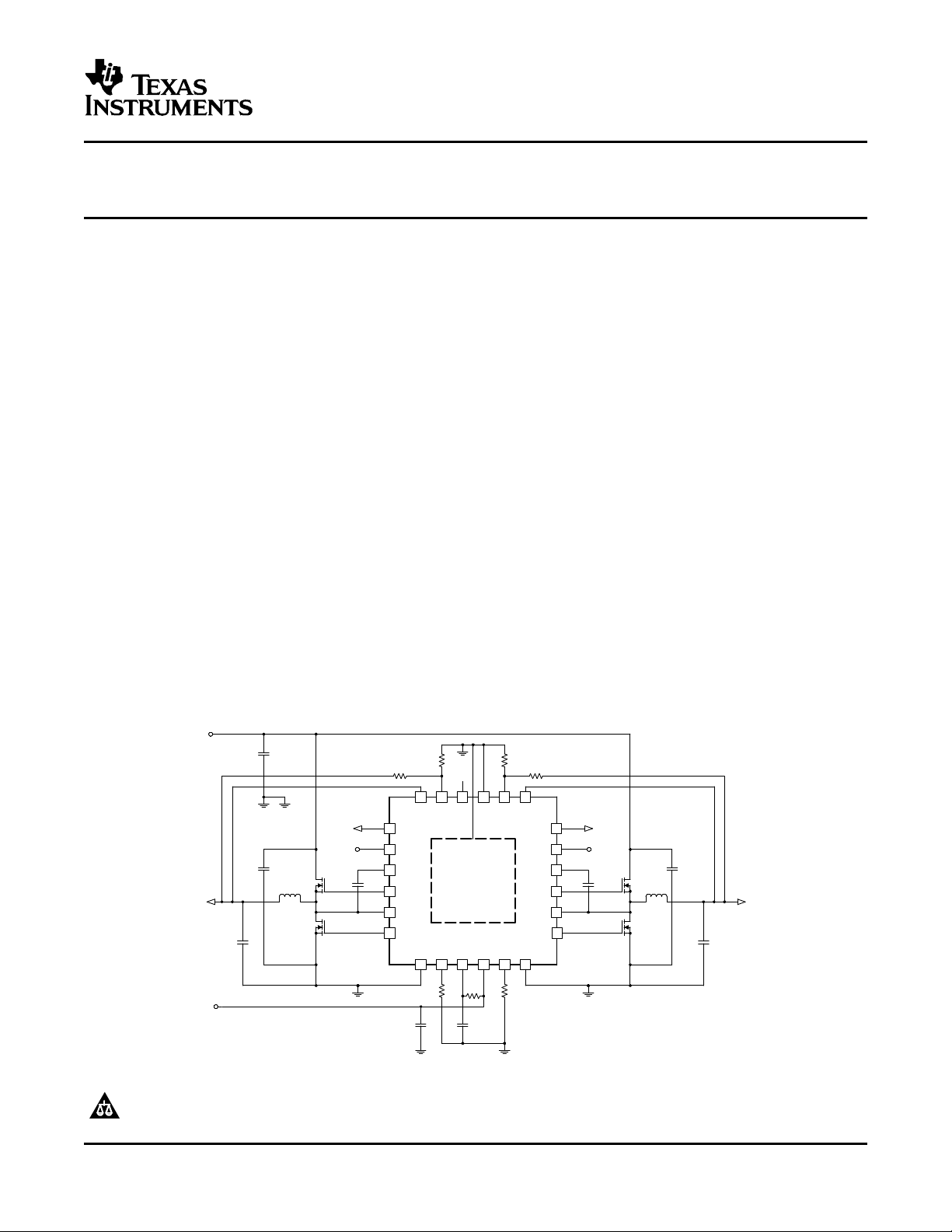
TPS51124 - DUAL SYNCHRONOUS STEP-DOWN CONTROLLER FOR LOW VOLTAGE POWER RAILS
Table of contents
 Loading...
Datasheet TPS51124 - DUAL SYNCHRONOUS STEP-DOWN CONTROLLER FOR LOW VOLTAGE POWER RAILS Datasheet
Page 1
www.ti.com
75 kΩ
9
10
11
12
PGOOD1
EN1
PGOOD2
EN2
TPS51124RGE
(QFN24)
13 14 15 16
VBST1
DRVL1
LL1
DRVH1
VBST2
DRVH2
LL2
DRVL2
17
8
7
6 5 4 3 2 1
18
19
20
21
22
23
24
VO1
1.05 V/10 A
Q2
IRF8113
L1
Q1
IRF7821
VO2
1.5 V/10 A
Q4
IRF8113
L2
Q3
IRF7821
Input Voltage
3 V to 28 V
PowerPAD
TM
C7
R6
C3
C1
C6
C4
R3
6.8
C8
R7
R1
R2
75
R5
R4
V5IN
4.5 V to 5.5 V
VO2
VO1
VFB2
TONSEL
GND
VFB1
PGND2
TRIP2
V5FILT
V5IN
TRIP1
PGND1
Power
Good2
EN2
C5
C2
Power
Good1
EN1
SGND
PGNDPGND
SGND
C9
SGND PGND
PGND
73.2 kΩ
kΩ
28.7 kΩ
22 µF
2 x 330 µF
1 µH
10 µF
0.1 µF
4.7 μF
6.8 kΩ
1 μF
3.3Ω
kΩ
0.1 µF
10 µF
1 µH
2 x 330 µF
DUAL SYNCHRONOUS STEP-DOWN CONTROLLER FOR
LOW VOLTAGE POWER RAILS
FEATURES DESCRIPTION
• High Efficiency, Low-Power Consumption,
Shutdowns to <1 µ A
• Fixed Frequency Emulated On-Time Control,
Frequency Selectable From Three Options
• D-CAP™ Mode Enables Fast Transient
Response
• Auto-Skip Mode
• Less Than 1% Initial Reference Accuracy
• Low Output Ripple
• Wide Input Voltage Range: 3 V to 28 V
• Output Voltage Range: 0.76 V to 5.5 V
• Low-Side R
• Adaptive Gate Drivers With Integrated Boost
Diode
• Internal 1.2-ms Voltage-Servo Soft Start
• Power-Good Signals for Each Channel With
Delay Timer
• Output Discharge During Disable, Fault
APPLICATIONS
• Notebook I/O and Low Voltage System Bus
DS(ON)
Loss-less Current Sensing
TPS51124
SLVS616A – NOVEMBER 2005 – REVISED NOVEMBER 2005
The TPS51124 is a dual, adaptive on-time D-CAP™
mode synchronous buck controller. The part enables
system designers to cost effectively complete the
suite of notebook power bus regulators with the
absolute lowest external component count and lowest
standby consumption. The fixed frequency emulated
adaptive on-time control supports seamless operation
between PWM mode at heavy load condition and
reduced frequency operation at light load for high
efficiency down to milliampere range. The main
control loop for the TPS51124 uses the D-CAP mode
that optimized for low ESR output capacitors such as
POSCAP or SP-CAP promises fast transient
response with no external compensation. Simple and
separate power good signals for each channel allow
flexibility of power sequencing. The part provides a
convenient and efficient operation with supply input
voltages (V5IN, V5FILT) ranging from 4.5 V to 5.5 V,
conversion voltages (drain voltage for the
synchronous high-side MOSFET) from 3 V to 28 V
and output voltages from 0.76 V to 5.5 V.
The TPS51124 is available in 24-pin QFN package
specified from –40 ° C to 85 ° C ambient temperature
range.
Please be aware that an important notice concerning availability, standard warranty, and use in critical applications of Texas
Instruments semiconductor products and disclaimers thereto appears at the end of this data sheet.
D-CAP, PowerPAD are trademarks of Texas Instruments.
PRODUCTION DATA information is current as of publication date.
Products conform to specifications per the terms of the Texas
Instruments standard warranty. Production processing does not
necessarily include testing of all parameters.
Copyright © 2005, Texas Instruments Incorporated
Page 2
www.ti.com
TPS51124
SLVS616A – NOVEMBER 2005 – REVISED NOVEMBER 2005
These devices have limited built-in ESD protection. The leads should be shorted together or the device
placed in conductive foam during storage or handling to prevent electrostatic damage to the MOS gates.
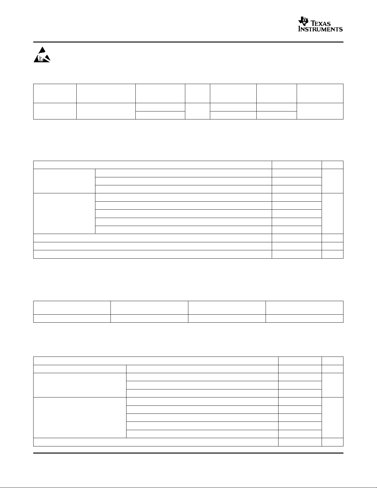
ORDERING INFORMATION
T
A
–40 ° C to 85 ° C 24
(1) All packaging options have Cu NIPDAU lead/ball finish.
PACKAGE PART PINS ORDER ECO PLAN
Plastic Quad TPS51124RGET Tape-and-Reel 250
Flat Pack (QFN)
ABSOLUTE MAXIMUM RATINGS
ORDERING MINIMUM
NUMBER QUANTITY
TPS51124RGER Tape-and-Reel 3000
(1)
(1)
OUTPUT
SUPPLY
Green (RoHS and
over operating free-air temperature range (unless otherwise noted)
VALUE UNIT
Input voltage
range
Output voltage
range
T
T
T
(1) Stresses beyond those listed under absolute maximum ratings may cause permanent damage to the device. These are stress ratings
Operating ambient temperature range –40 to 85 ° C
A
Storage temperature range –55 to 150 ° C
stg
Junction temperature range –40 to 125 ° C
J
only and functional operation of the device at these or any other conditions beyond those indicated under recommended operating
conditions is not implied. Exposure to absolute-maximum-rated conditions for extended periods may affect device reliability. All voltage
values are with respect to the network ground terminal unless otherwise noted
VBST1, VBST2 –0.3 to 36
VBST1, VBST2 (wrt LLx) –0.3 to 6 V
V5IN, V5FILT, EN1, EN2, VFB1, VFB2, TRIP1, TRIP2, VO1, VO2, TONSEL –0.3 to 6
DRVH1, DRVH2 –1 to 36
DRVH1, DRVH2 (wrt LLx) –0.3 to 6
LL1, LL2 –2 to 30 V
PGOOD1, PGOOD2, DRVL1, DRVL2 –0.3 to 6
PGND1, PGND2 –0.3 to 0.3
no Sb/Br)
DISSIPATION RATINGS
PACKAGE TA<25 ° C DERATING FACTOR TA= 85 ° C
24-pin QFN
(1) Enhanced thermal conductance by 2 × 2 thermal vias beneath thermal pad.
(1)
POWER RATING ABOVE TA= 25 ° C POWER RATING
2.33 W 23.3 mW/ ° C 0.93 W
RECOMMENDED OPERATING CONDITIONS
over operating free-air temperature range (unless otherwise noted)
Supply input voltage range V5IN, V5FILT 4.5 5.5 V
VBST1, VBST2 –0.1 34
Input voltage range VBST1, VBST2 (wrt LLx) –0.1 5.5 V
EN1, EN2, VFB1, VFB2, TRIP1, TRIP2, VO1, VO2, TONSEL –0.1 5.5
DRVH1, DRVH2 –0.8 34
DRVH1, DRVH2 (wrt LLx) –0.1 5.5
Output voltage range LL1, LL2 –1.8 28 V
PGOOD1, PGOOD2, DRVL1, DRVL2 –0.1 5.5
PGND1, PGND2 –0.1 0.1
T
Operating ambient temperature range –40 85 ° C
A
2
MIN MAX UNIT
Page 3
www.ti.com
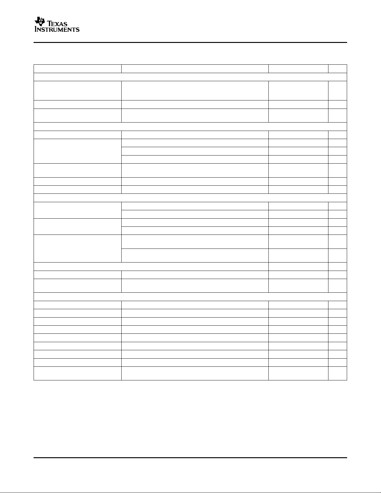
ELECTRICAL CHARACTERISTICS
over operating free-air temperature range, V5IN = V5FILT = 5 V (unless otherwise noted)
PARAMETER TEST CONDITIONS MIN TYP MAX UNIT
SUPPLY CURRENT
I
V5FILT
I
V5INSDN
I
V5FILTSD
N
V5FILT supply current EN1 = EN2 = 5 V, VFB1 = VFB2 = 0.77 V, 350 700 µ A
V5IN shutdown current V5IN current, no load, EN1 = EN2 = 0 V 1 µ A
V5FILT shutdown current V5FILT current, no load, EN1 = EN2 = 0 V 1 µ A
VFB VOLTAGE and DISCHARGE RESISTANCE
V
VFB
V
VFB
V
VFBSKIP
I
VFB
R
Dischg
VFB regulation voltage FB voltage, skip mode (f
VFB regulation voltage
tolerance
VFB regulation shift in 0.758-V target for resistor divider. See PWM Operation of
continuous conduction Detailed Description
VFB input current VFBx = 0.758 V, absolute value 0.02 0.1 µ A
VO discharge resistance ENx = 0 V, VOx = 0.5 V, TA= 25 ° C 10 20 Ω
OUTPUT: N-CHANEEL MOSFET GATE DRIVERS
R
DRVH
R
DRVL
T
D
DRVH resistance
DRVL resistance
Dead time
INTERNAL BST DIODE
V
FBST
I
VBSTLK
Forward voltage V
VBST leakage current 0.1 1 µ A
ON-TIME TIMER CONTROL AND INTERNAL SOFT START,
T
ON11
T
ON12
T
ON13
T
ON21
T
ON22
T
ON23
T
ON(MIN)
T
OFF(MIN)
T
ss
CH1, 240-kHz setting VO1 = 1.5 V,TONSEL = GND, LL1 = 12 V 440 500 560 ns
CH1, 300-kHz setting VO1 = 1.5 V, TONSEL = FLOAT, LL1 = 12 V 340 390 440 ns
CH1, 360-kHz setting VO1 = 1.5 V,TONSEL = V5FILT, LL1 = 12 V 265 305 345 ns
CH2, 300-kHz setting VO2 = 1.05 V, TONSEL = GND, LL2 = 12 V 235 270 305 ns
CH2, 360-kHz setting VO2 = 1.05 V, TONSEL = FLOAT, LL2 = 12 V 180 210 240 ns
CH2, 420-kHz setting VO2 = 1.05 V, TONSEL = V5FILT, LL2 = 12 V 120 150 180 ns
CH2 On time VO2 = 0.76 V, TONSEL = V5FILT, LL2 = 28 V 80 110 140 ns
CH1/CH2 Min. off time LL = –0.1 V, TA= 25 ° C, VFB = 0.7 V 435 ns
Internal SS time 0.85 1.2 1.40 ms
(1) Ensured by design. Not production tested.
V5FILT current, no load,
LL1=LL2=0.5V
/10) 764 mV
PWM
TA= 25 ° C, bandgap initial accuracy –0.9% 0.9%
TA= 0 ° C to 85 ° C
TA= –40 ° C to 85 ° C
Source, V
Sink, V
DRVHx-LLx
Source, V
Sink, V
DRVLx–PGNDx
(1)
(1)
(1)
VBSTx–DRVHx
= 0.5 V 5 7 Ω
= 0.5 V 1.5 2.5 Ω
V5IN–DRVLx
= 0.5 V 4 6 Ω
= 0.5 V 1 2.0 Ω
DRVHx-low (DRVHx = 1 V) to DRVLx-on
(DRVLx = 4 V), LL = –0.05 V,
DRVLx-low (DRVLx = 1 V) to DRVHx-on
(DRVHx = 4 V), LL = –0.05 V,
V5IN–VBSTx
, IF= 10 mA, TA= 25 ° C 0.7 0.8 0.9 V
VBST = 34 V, LL = 28 V, VOx = 5.5 V,
TA= 25 ° C
Internal soft start, time from ENx > 3 V to VFBx regulation value
= 735 mV
TPS51124
SLVS616A – NOVEMBER 2005 – REVISED NOVEMBER 2005
–1.3% 1.3%
–1.6% 1.6%
758 mV
10 20 50 ns
30 40 60 ns
3
Page 4
www.ti.com
TPS51124
SLVS616A – NOVEMBER 2005 – REVISED NOVEMBER 2005
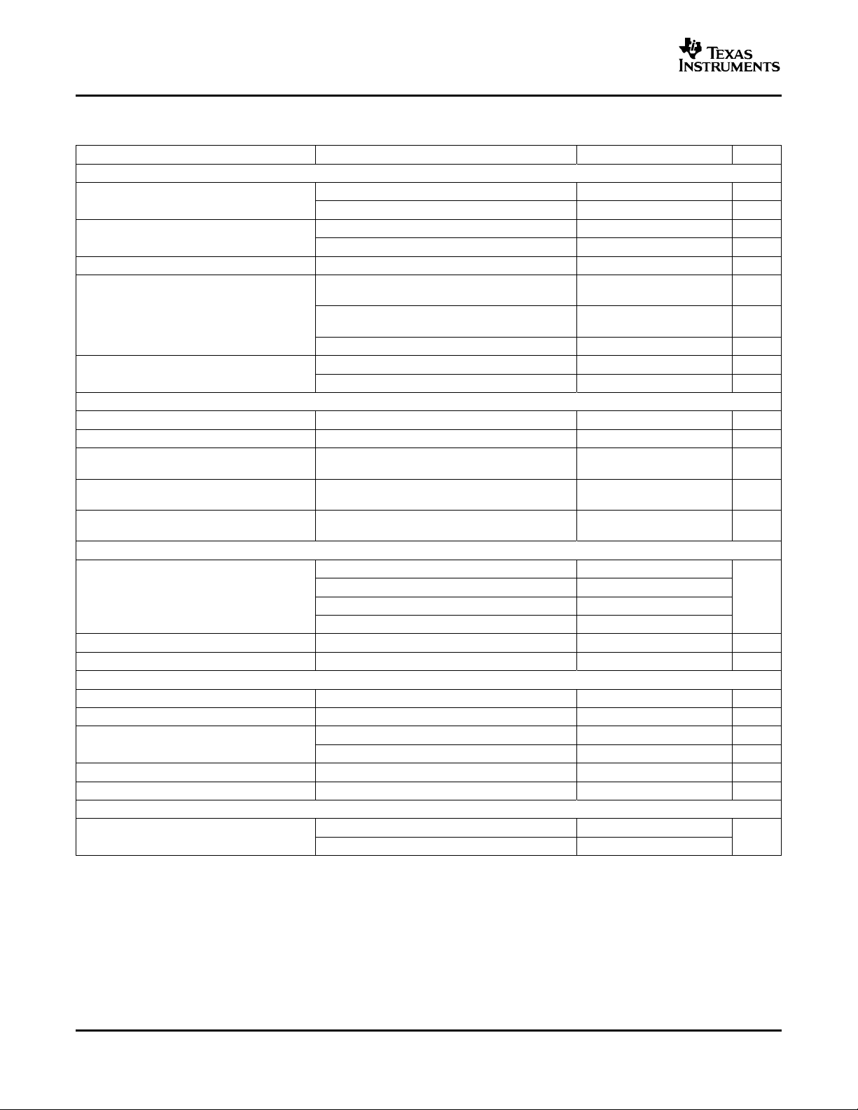
ELECTRICAL CHARACTERISTICS (Continued)
over operating free-air temperature range, V5IN = V5FILT = 5 V (unless otherwise noted)
PARAMETER TEST CONDITIONS MIN TYP MAX UNIT
UVLO/LOGIC THRESHOLD
V
UV5VFILT
V
EN
I
EN
V
TONSEL
I
TONSEL
V5FILT UVLO threshold
ENx threshold
ENx input current Absolute value
TONSEL threshold Medium
TONSEL input current
CURRENT SENSE
I
TRIP
TC
ITRIP
V
OCLoff
V
ZC
V
Rtrip
TRIP source current VTRIPx < 0.3 V, TA= 25 ° C 9 10 11 µ A
I
temperature coeffficent On the basis of 25 ° C
TRIP
OCP compensation offset –10 0 10 mV
Zero cross detection comparator VPGNDx-LLx voltage, PGOODx = Hi
offset
Current limit threshold setting V
range
POWER-GOOD COMPARATOR
V
THPG
I
PGMAX
T
PGDEL
PG threshold
PG sink current PGOODx = 0.5 V 2.5 5.0 mA
PG delay Delay for PG in 400 510 620 µ s
OUTPUT UNDERVOLTAGE AND OVERVOLTAGE PROTECTION
V
OVP
T
OVPDEL
V
UVP
T
UVPDEL
T
UVPEN
Output OVP trip threshold OVP detect 110% 115% 120%
Output OVP prop delay 1.5 µ s
Output UVP trip threshold
Output UVP delay 20 32 40 µ s
Output UVP enable delay After 1.7 × Tss, UVP protection engaged 1.4 2 2.4 ms
THERMAL SHUTDOWN
T
SDN
Thermal shutdown threshold ° C
Wake up 3.7 4.0 4.3 V
Hysteresis 0.2 0.3 0.4 V
Wake up 1.0 1.3 1.5 V
Hysteresis 0.2 V
(1)
(1)
Fast
(1)
(1)
Slow
TONSEL=0V, current out of the pin
TONSEL=5V, current in to the pin
(1)
(V
TRIPx-GND
V
TRIPx-GND
TRIPx-GND
– V
PGNDx-LLx
= 60 mV
) voltage,
voltage, all temperatures
(1)
PG in from lower (PGOODx goes hi) 92.5% 95% 97.5%
PG low hysteresis (PGOODx goes low) –5%
PG in from higher (PGOODx goes hi) 102.5% 105% 107.5%
PG high hysteresis (PGOODx goes low) 5%
UVP detect 65% 70% 75%
Hysteresis (recovery < 20 µ s) 10%
Shutdown temperature
Hysteresis
(1)
(1)
0.02 0.1 µ A
V5FILT
–0.3
2 V
V5FILT
–1.0
V
0.5 V
(1)
1 µ A
1 µ A
4200 ppm/ ° C
(1)
(1)
30 200 mV
0.5 mV
160
10
(1) Ensured by design. Not production tested.
4
Page 5
www.ti.com
PGOOD1
EN1
VBST1
DR VH1
LL1
DR VL1
24 23 22 21 20 19
PGND1
TRIP1
V5IN
V5FILT
TRIP2
PGND2
VO1
VFB1
GND
TONSEL
VFB2
VO2
48
17
16
15
14
13
1
2
3
4
5
6
PGOOD2
EN2
VBST2
DR VH2
LL2
DR VL2
7 8 9 10 11 12
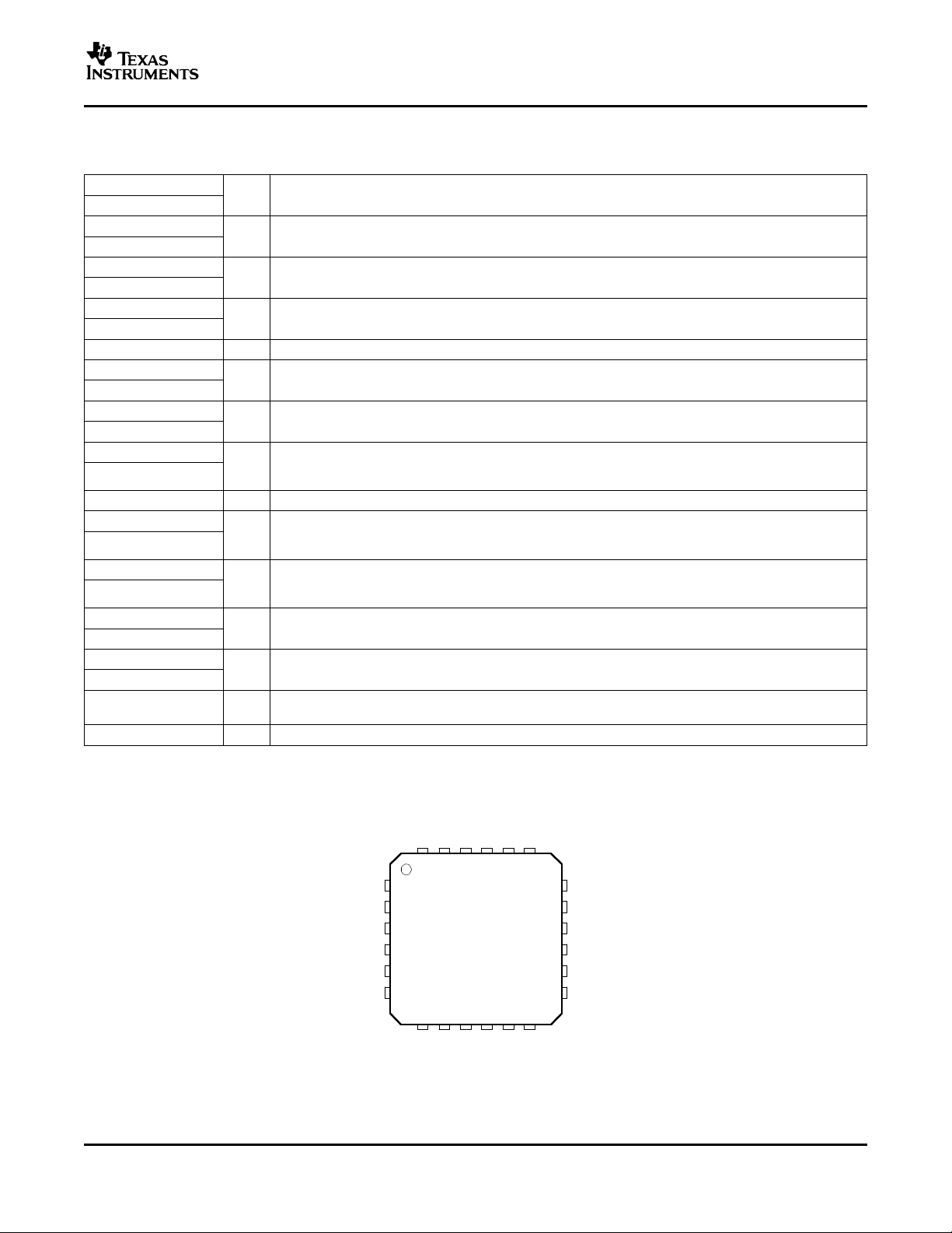
QFN PACKAGE
(TOP VIEW)
TPS51124
SLVS616A – NOVEMBER 2005 – REVISED NOVEMBER 2005
DEVICE INFORMATION
TERMINAL FUNCTIONS
TERMINAL
NAME NO.
DRVH1 21
DRVH2 10
DRVL1 19
DRVL2 12
EN1 23
EN2 8
GND 3 I Signal ground pin
LL1 20
LL2 11
PGND1 18
PGND2 13
PGOOD1 24 Power Good window comparator open drain output for channel 1 and 2. Pull up with a resistor to 5 V, or
PGOOD2 7
TONSEL 4 I On-time selection pin. See Table 1 .
TRIP1 17 Over-current trip point set input. Connect resistor from this pin to GND to set threshold for synchronous
TRIP2 14
VBST1 22 Supply input for synchronous high-side MOSFET driver (Boost Terminal). Connect capacitor from this pin
VBST2 9
VFB1 2
VFB2 5
VO1 1
VO2 6
V5FILT 15 I
V5IN 16 I 5-V power supply input for FET gate drivers. Internally connected to VBSTx by PN diodes.
I/O DESCRIPTION
Synchronous high-side MOSFET driver outputs. LL node referenced floating drivers. The gate drive
O
voltage is defined by the voltage across VBST to LL node flying capacitor.
Synchronous low-side MOSFET driver outputs. PGND referenced drivers. The gate drive voltage is
O
defined by V5IN voltage.
I Channel 1 and channel 2 enable pins. Connect to 5 V or 3.3 V to turn on SMPS
Switch node connections for high-side drivers return. Also serve as input to current comparators and input
I/O
voltage monitor for on-time control circuitry.
Ground returns for DRVL1 and DRVL2. Also serve as input of current comparators. Connect PGND1,
I/O
PGND2, and GND strongly together near the IC. Output discharge current flows through this pin, also.
O appropriate signal voltage. Current capability is 5 mA. PGOOD goes high 0.5 ms after VFB comes within
specified limits. Power bad, or the terminal goes low, is within 10 µ s.
I low-side R
over-current comparator.
sense. Voltage across this pin and GND is compared to voltage across PGND and LL at
DS(on)
I to respective LL terminals. An internal PN diode is connected between V5IN to each of these pins. User
can add external Schottky diode if forward drop is critical to drive the MOSFET.
I SMPS voltage feedback inputs. Connect with feedback resistor divider.
Output connections to SMPS. These terminals serve two functions: On-time adjustment and output
I
discharge.
5-V power supply input for the entire control circuit except the MOSFET drivers. Connect RC low-pass
filter from V5IN to V5FILT.
5
Page 6
www.ti.com
−30%
UV
OV
+15%
Ref
758 mV
SSx
VFBx
TRIPx
10 µA
GND
LLx
PGNDx
LLx
VOx
LLx
PGNDx
LLx
ONx
ZC
OCP
PWM
+5/10%
−5/10%
Control Logic
1
Shot
On/Off T ime
Minimum On/Off
Light Load,
OVP/UVP,
Discharge
Control
PGNDx
Delay
XCON
T ONSEL
Sdn
Fault
DR VLx
V5IN
V5IN
LLx
DR VHx
VBSTx
THOK
V5OK
PGNDx
PGOODx
V5IN
4 V/3.7 V
V5OK
THOK
BGR
V5FIL T
VO1
VBST1
DR VH1
LL1
DR VL1
PGND1
Switcher Controller
V5DRV
Ref
Fault
Sdn
ON1
SS1
ANALOG/SUB GND
EN/SS
Control
TRIP1
VFB1
PGOOD1
EN1
EN2
GND
PGOOD2
VFB2
TRIP2
SS2
ON2
Sdn
Fault
Ref
V5DRV
Switcher Controller
VO2
VBST2
DR VH2
LL2LL2
DR VL2
PGND2
1 V
T ONSEL
4 V
Frequency Control
FAST
SLOW
160 °C/
150 °C
MID
TPS51124
SLVS616A – NOVEMBER 2005 – REVISED NOVEMBER 2005
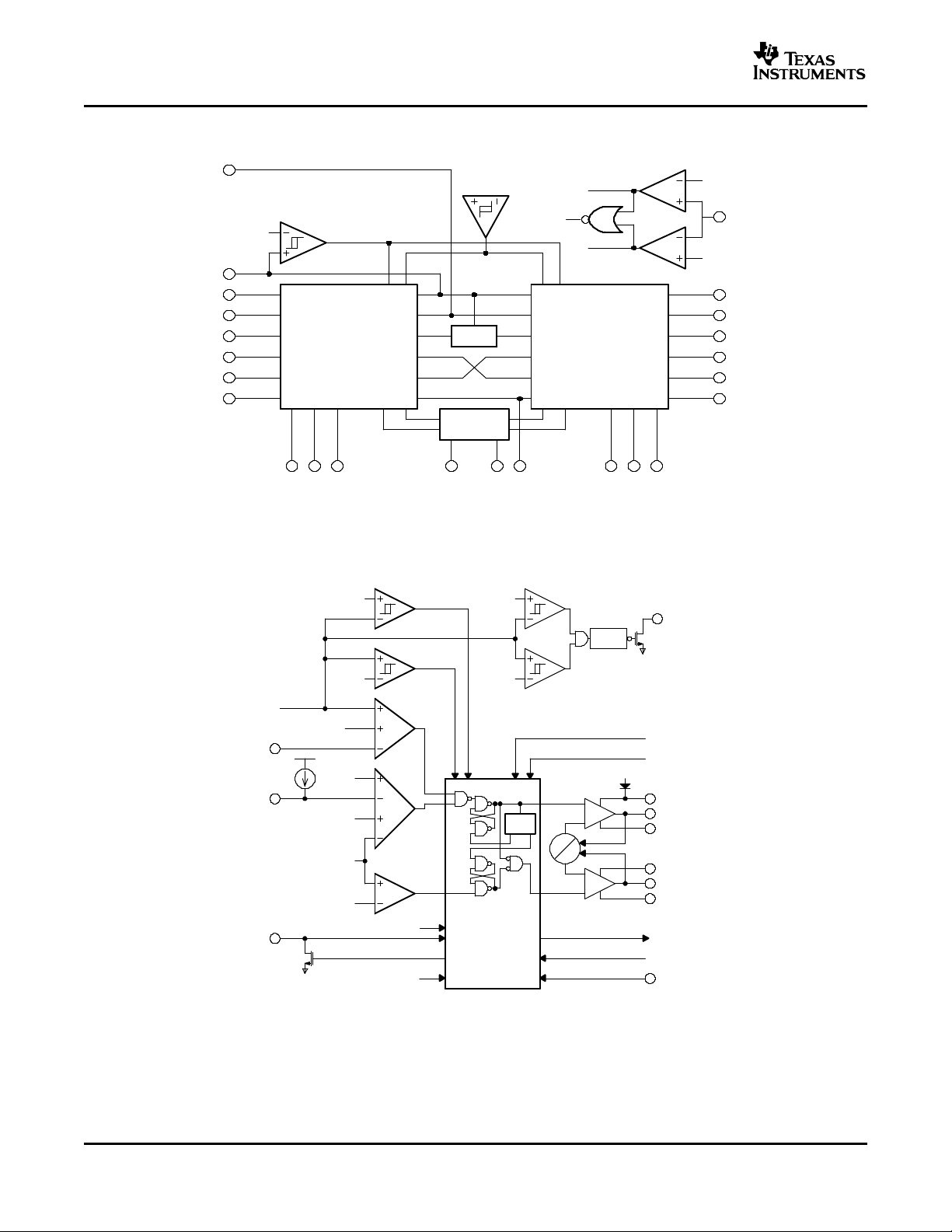
FUNCTIONAL BLOCK DIAGRAM
6
Page 7

www.ti.com
I
OUT(LL)
1
2 L ƒ
VIn V
OUT
V
OUT
V
IN
TPS51124
SLVS616A – NOVEMBER 2005 – REVISED NOVEMBER 2005
DETAILED DESCRIPTION
PWM OPERATION
The main control loop of the switching mode power supply (SMPS) is designed as an adaptive on-time pulse
width modulation (PWM) controller. It supports a proprietary D-CAP Mode. D-CAP Mode uses an internal
compensation circuit and is suitable for low external component-count configuration, with appropriate amount of
ESR at the output capacitor(s). The output voltage is monitored at a feedback point voltage. The reference
voltage at the feedback point is a combination of a fixed 0.750-V precision reference and a synchronized,
precision 15-mV ramp signal. Lower output voltages in notebook systems (e.g., 1.05 V, 1.5 V) require extremely
low output ripple. By providing a ramp signal, the TPS51124 is easier to use in low-output ripple systems. The
combination of the precision ramp and reference yield an effective target reference of 0.758 V. The accuracy of
this effective reference remains 1.3% over line and temperature.
At the beginning of each cycle, the synchronous high-side MOSFET is turned on, or becomes ON state. This
MOSFET is turned off, or becomes OFF state, after the internal one-shot timer expires. This one shot is
determined by the converter’s input voltage, VIN, and the output voltage, VOUT, to keep the frequency fairly
constant over the input voltage range; hence, it is called adaptive on-time control (see PWM Frequency and
Adaptive On-time Control). The high-side MOSFET is turned on again when feedback information indicates
insufficient output voltage, and inductor current information indicates a below-the-over-current limit condition.
Repeating operation in this manner, the controller regulates the output voltage. The synchronous low-side
MOSFET is turned on each OFF state to keep the conduction loss at a minimum. The low-side MOSFET is
turned off when the inductor current information detects zero level. This enables seamless transition to the
reduced frequency operation at light-load conditions so that high efficiency is kept over a broad range of load
current.
LIGHT-LOAD CONDITION
TPS51124 automatically reduces switching frequency at light-load conditions to maintain high efficiency. This
reduction of frequency is achieved smoothly and without increase of Vout ripple or load regulation. Detail
operation is described as follows. As the output current decreases from heavy-load condition, the inductor
current is also reduced, and eventually comes to the point that its valley touches zero current, which is the
boundary between continuous conduction and discontinuous conduction modes. The low-side MOSFET is turned
off when this zero inductor current is detected. As the load current is further decreased, the converter runs in
discontinuous conduction mode and it takes longer and longer to discharge the output capacitor to the level that
requires the next ON cycle. The ON time is kept the same as that in the heavy-load condition. In reverse, when
the output current increases from light load to heavy load, the switching frequency increases to the preset value
as the inductor current reaches the continuous conduction. The transition load point to the light-load operation,
I
OUT(LL)
where f is the PWM switching frequency.
Switching frequency versus output current in the light-load condition is a function of L, f, Vin, and Vout, but it
decreases almost proportional to the output current from the I
It should be noted that in the PWM control path is a small ramp . This ramp is transparent in normal, continuous
conduction mode and does not measurably affect the regulation voltage. However, in discontinuous, light-load
mode, an upward shift in regulation voltage of about 0.75% will be observed. The variation of this shift minimally
affects the reference tolerance. Therefore, the reference value in skip mode is 0.764 V ± 1.3% over line and
temperature.
(i.e., the threshold between continuous and discontinuous conduction mode) can be calculated as follows;
OUT(LL)
given in Equation 1 .
(1)
7
Page 8
www.ti.com
TPS51124
SLVS616A – NOVEMBER 2005 – REVISED NOVEMBER 2005
DETAILED DESCRIPTION (continued)
LOW-SIDE DRIVER
The low-side driver is designed to drive high current low R
represented by its internal resistances, which are 4 Ω for V5IN to DRVLx, and 1 Ω for DRVLx to PGNDx. A dead
time to prevent shoot through is internally generated between high-side MOSFET off to low-side MOSFET on,
and low-side MOSFET off to high-side MOSFET on. A 5-V bias voltage is delivered from V5IN supply. The
instantaneous drive current is supplied by an input capacitor connected between V5IN and GND. The average
drive current is equal to the gate charge at Vgs = 5 V times switching frequency. This gate drive current, as well
as the high-side gate drive current times 5 V, makes the driving power that needs to be dissipated from
TPS51124 package.
HIGH-SIDE DRIVER
The high-side driver is designed to drive high-current, low R
floating driver, 5-V bias voltage is delivered from V5IN supply. The average drive current is also calculated by the
gate charge at Vgs = 5 V times switching frequency. The instantaneous drive current is supplied by the flying
capacitor between VBSTx and LLx pins. The drive capability is represented by its internal resistances, which are
5 Ω for VBSTx to DRVHx and 1.5 Ω for DRVHx to LLx.
PWM FREQUENCY AND ADAPTIVE ON-TIME CONTROL
TPS51124 employs adaptive on-time control scheme and does not have a dedicated oscillator on board.
However, the part runs with pseudo-constant frequency by feed-forwarding the input and output voltage into the
on-time one-shot timer. The frequencies are set by TONSEL terminal connection as Table 1 . The on-time is
controlled inverse proportional to the input voltage and proportional to the output voltage so that the duty ratio is
kept as VOUT/VIN technically with the same cycle time. Although the TPS51124 does not have a pin connected
to VIN, the input voltage is monitored at LLx pin during the ON state. This helps pin count reduction to make the
part compact without sacrificing its performance.
N-channel MOSFET(s). The drive capability is
DS(on)
N-channel MOSFET(s). When configured as a
DS(on)
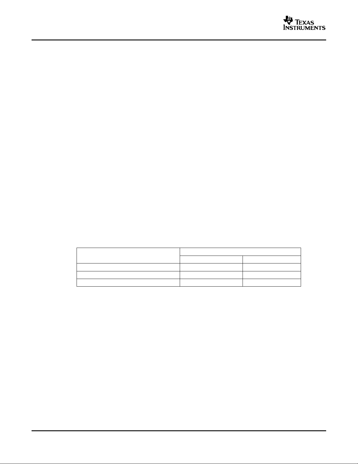
Table 1. TONSEL Connection and Switching Frequency Table
(Frequencies Are Approximate)
TONSEL CONNECTION SWITCHING FREQUENCY
CH1 CH2
GND 240 kHz 300 kHz
FLOAT (Open) 300 kHz 360 kHz
V5FILT 360 kHz 420 kHz
SOFT START
The TPS51124 has an internal, 1.2-ms, voltage servo soft start for each channel. When the ENx pin becomes
high, an internal DAC begins ramping up the reference voltage to the PWM comparator. Smooth control of the
output voltage is maintained during start-up. As TPS51124 shares one DAC with both channels, if ENx pin is set
to high while another channel is starting up, soft start is postponed until another channel soft start has
completed. If both of EN1 and EN2 are set high at a same time, both channels start up at same time.
POWER GOOD
The TPS51124 has power-good output for both switcher channels. The power-good function is activated after
soft start has finished. If the output voltage becomes within ± 5% of the target value, internal comparators detect
power good state and the power good signal becomes high after a 510- µ s internal delay. During start-up, this
internal delay starts after 1.7 times internal soft-start time to avoid a glitch of power-good signal. If the feedback
voltage goes outside of ± 10% of the target value, the power-good signal becomes low after 10- µ s internal delay.
Also note that if the feedback voltage goes +10% above target value and the power-good signal flags low, then
the loop attempts to correct the output by turning on the low-side driver (forced PWM mode). After the feedback
voltage returns to be within +5% of the target value and the power-good signal goes high, the controller returns
back to auto-skip mode.
8
Page 9

www.ti.com
V
trip
(mV) R
trip
(k) 10 (A)
I
ocl
V
tripRDS(on)
I
ripple
2
V
trip
R
DS(on)
1
2 L ƒ
VIN V
OUT
V
OUT
V
IN
TPS51124
SLVS616A – NOVEMBER 2005 – REVISED NOVEMBER 2005
DETAILED DESCRIPTION (continued)
OUTPUT DISCHARGE CONTROL
TPS51124 discharges the output when ENx is low, or the controller is turned off by the protection functions
(OVP, UVP, UVLO, and thermal shutdown). TPS51124 discharges outputs using an internal, 10- Ω MOSFET
which is connected to VOx and PGNDx. The external low-side MOSFET is not turned on for the output discharge
operation to avoid the possibility of causing negative voltage at the output. Output discharge time constant is a
function of the output capacitance and the resistance of the internal discharge MOSFET. This discharge ensures
that, on restart, the regulated voltage always starts from zero volts. In case a SMPS is restarted before discharge
completion, discharge is terminated and the switching resumes after the reference level, ramped up by an
internal DAC, comes back to the remaining output voltage.
CURRENT PROTECTION
TPS51124 has cycle-by-cycle over-current limiting control. The inductor current is monitored during the OFF
state and the controller keeps the OFF state during the inductor current is larger than the over-current trip level.
In order to provide both good accuracy and cost effective solution, TPS51124 supports temperature
compensated MOSFET R
resistor, R
. TRIPx terminal sources 10- µ A Itrip current and the trip level is set to the OCL trip voltage V
trip
below.
The trip level should be in the range of 30 mV to 200 mV over all operational temperatures. The inductor current
is monitored by the voltage between PGNDx pin and LLx pin so that LLx pin should be connected to the drain
terminal of the low-side MOSFET. Itrip has 4200 ppm/ ° C temperature slope to compensate the temperature
dependency of the R
DS(on)
connected to the source terminal of the low-side MOSFET. As the comparison is done during the OFF state, V
sets the valley level of the inductor current. Thus, the load current at over-current threshold, I
calculated as follows;
sensing. TRIPx pin should be connected to GND through the trip voltage setting
DS(on)
. PGNDx is used as the positive current sensing node so that PGNDx should be
, can be
ocl
trip
as
(2)
trip
In an over-current condition, the current to the load exceeds the current to the output capacitor; thus, the output
voltage tends to fall off (droop). Eventually, it ends up crossing the under-voltage protection threshold and shuts
down.
OVER/UNDER-VOLTAGE PROTECTION
TPS51124 monitors a resistor divided feedback voltage to detect over and under voltage. When the feedback
voltage becomes higher than 115% of the target voltage, the OVP comparator output goes high and the circuit
latches as the high-side MOSFET driver OFF and the low-side MOSFET driver ON.
Also, the TPS51124 monitors VOx voltage directly and if it becomes greater than 5.75 V, the TPS51124 turns off
the top MOSFET driver, and shuts off both drivers of the other channel.
When the feedback voltage becomes lower than 70% of the target voltage, the UVP comparator output goes
high and an internal UVP delay counter begins counting. After 32 µ s, TPS51124 latches OFF both top and
bottom MOSFET drivers, and shuts off both drivers of the other channel. This function is enabled after 1.7 times
soft-start delay time, approximately 2 ms, to ensure start-up properly.
UVLO PROTECTION
TPS51124 has V5FILT under-voltage lock-out protection (UVLO). When the V5FILT voltage is lower than UVLO
threshold voltage, the TPS51124 is shut off. This is non-latch protection.
THERMAL SHUTDOWN
TPS51124 monitors its own temperature. If the temperature exceeds the threshold value (typically 160 ° C), the
switchers are shut off as both DRVH and DRVL at low; the output discharge function is enabled. TPS51124 is
shut off. This is non-latch protection.
(3)
9
Page 10
www.ti.com
0
100
200
300
400
500
−50 0 50 100 150
I
V5FILT
− Supply Current − Aµ
TJ − Junction Temperature − C
0
0.2
0.4
0.6
0.8
1
−50 0 50 100 150
I
V5FLTSDN
− Shutdown Current − Aµ
TJ − Junction Temperature − C
0
2
4
6
8
10
12
14
16
−50 0 50 100 150
I
TRIP
− Trip Source Current − Aµ
TJ − Junction Temperature − C
0
0.2
0.4
0.6
0.8
1
−50 0 50 100 150
I
V5INSDN
− Shutdown Current − Aµ
TJ − Junction Temperature − C
TPS51124
SLVS616A – NOVEMBER 2005 – REVISED NOVEMBER 2005
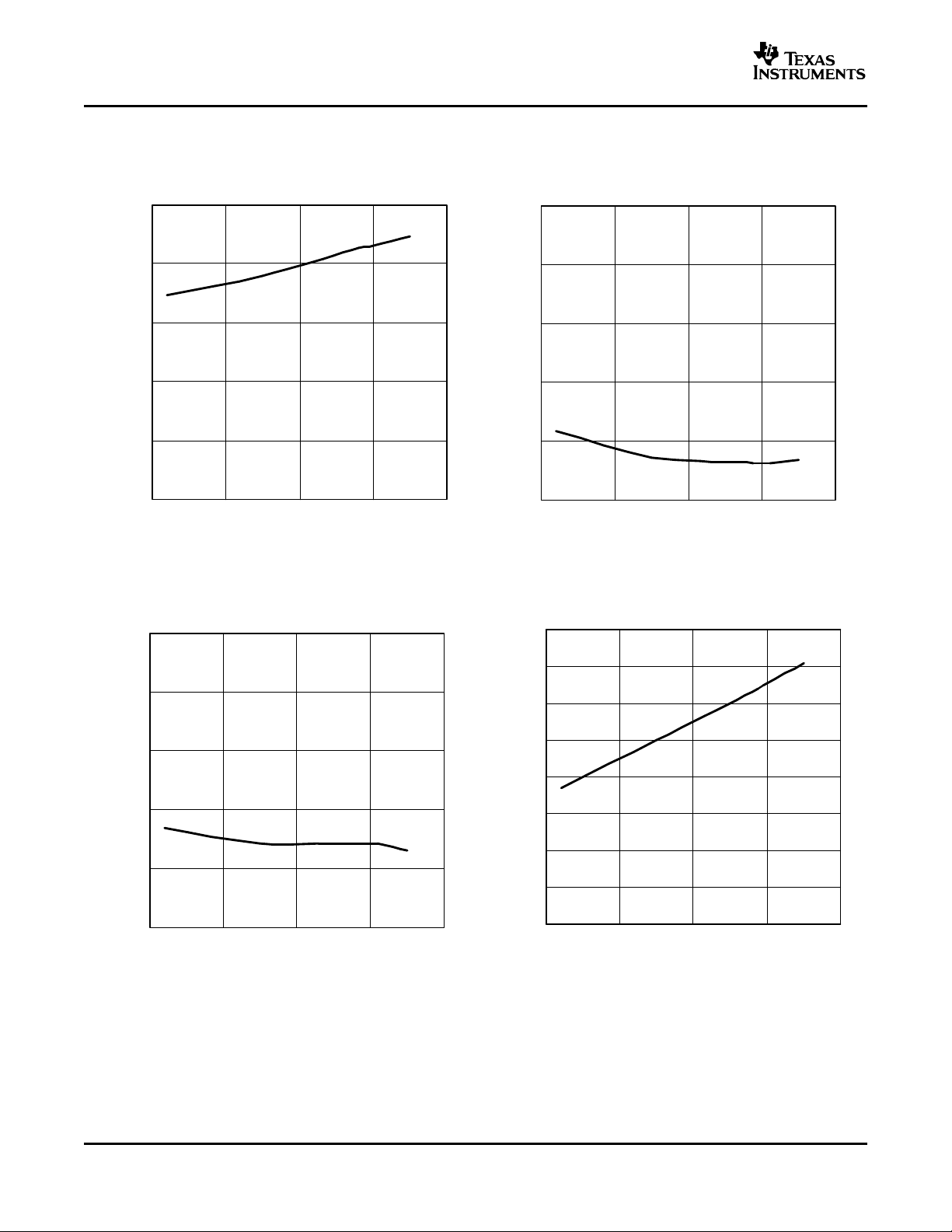
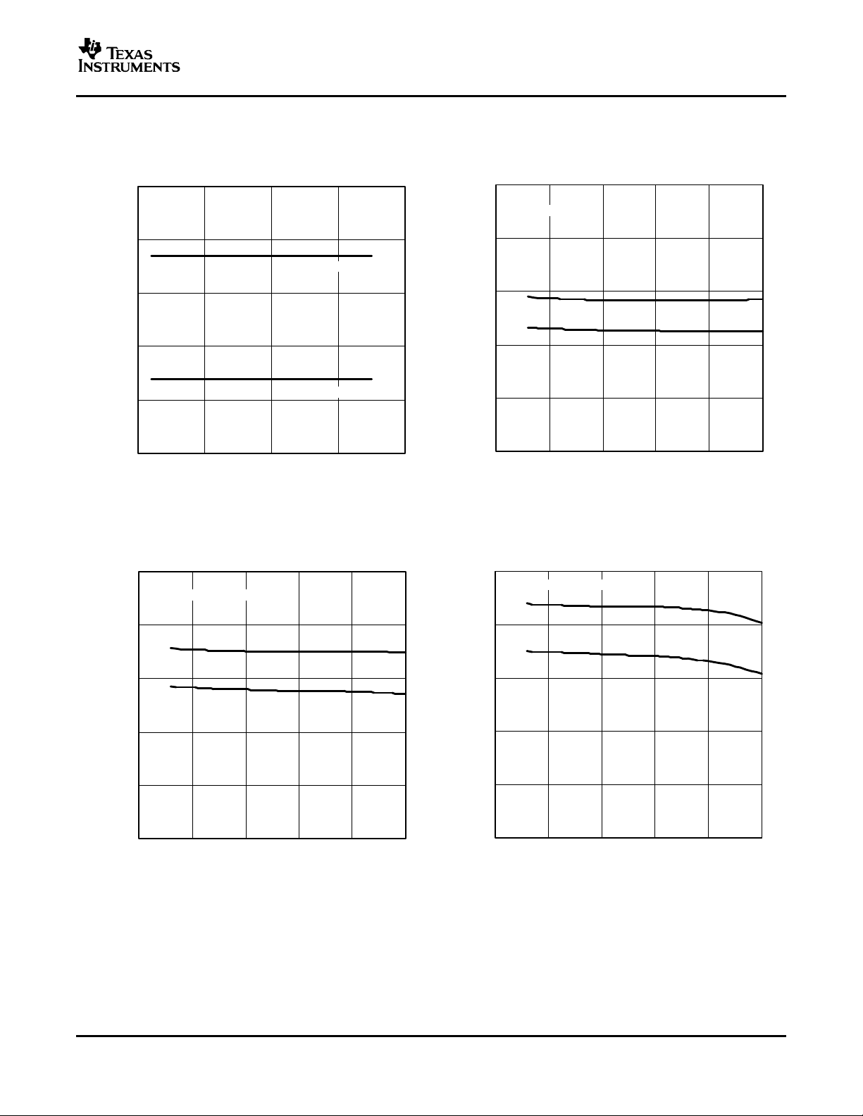
TYPICAL CHARACTERISTICS
V5FILT SUPPLY CURRENT V5FILT SHUTDOWN CURRENT
JUNCTION TEMPERATURE JUNCTION TEMPERATURE
V5IN SHUTDOWN CURRENT TRIP SOURCE CURRENT
JUNCTION TEMPERATURE JUNCTION TEMPERATURE
vs vs
Figure 1. Figure 2.
vs vs
10
Figure 3. Figure 4.
Page 11
www.ti.com
40
60
80
100
120
140
−50 0 50 100 150
V
OVP
V
UVP
− OVP/UVP Threshold − %
OVP
UVP
TJ − Junction Temperature − C
0
100
200
300
400
500
0 5 10 15 20 25
f
SW
− Switching Frequency − kHz
CH1
CH2
V
I
− Input Voltage V−
TONSEL = GND
0
100
200
300
400
500
0 5 10 15 20 25
CH1
CH2
TONSEL = FLOAT
f
SW
− Switching Frequency − kHz
VI− Input Voltage − V
0
100
200
300
400
500
0 5 10 15 20 25
CH1
CH2
TONSEL = V5FILT
f
SW
− Switching Frequency − kHz
VI− Input Voltage − V
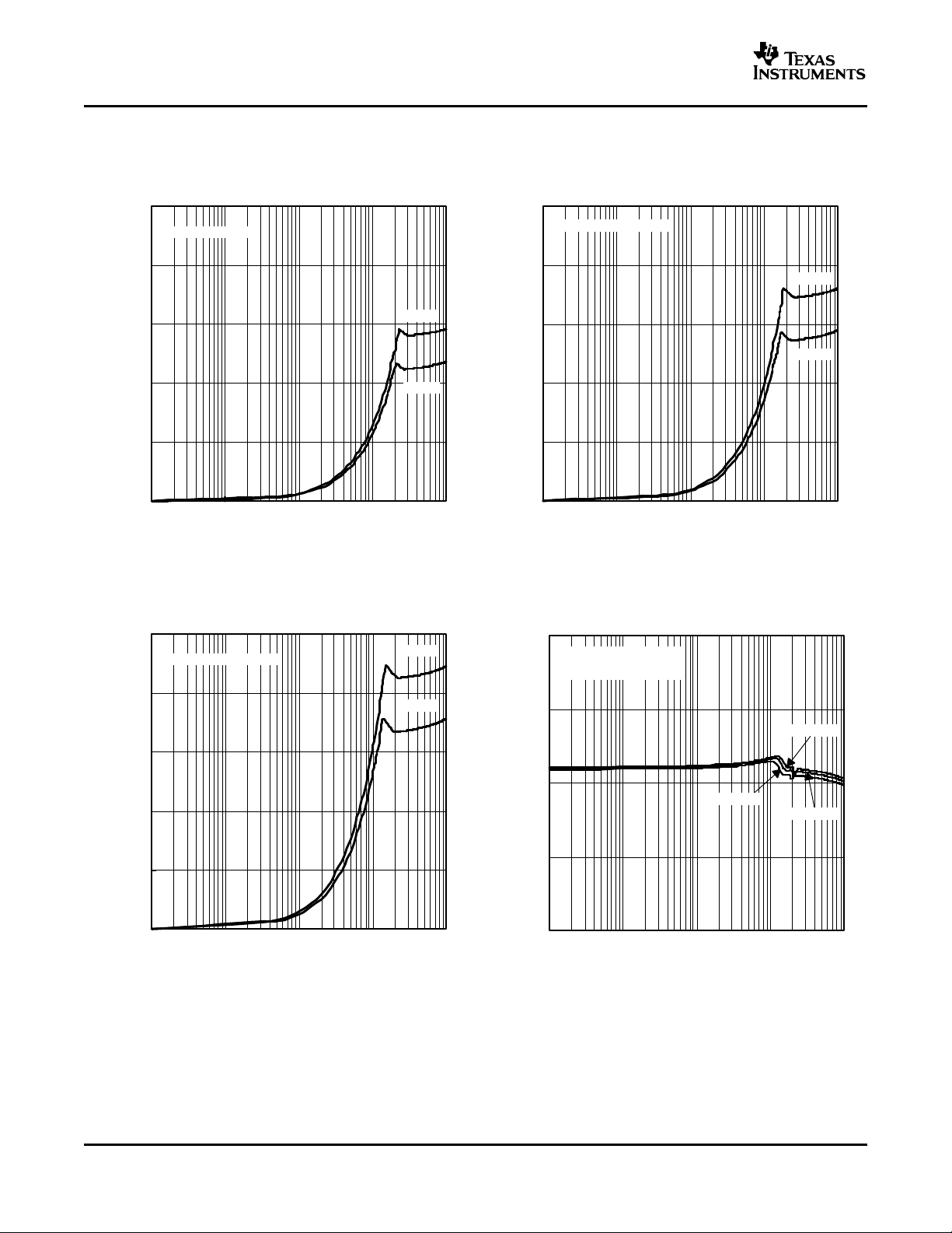
TYPICAL CHARACTERISTICS (continued)
TPS51124
SLVS616A – NOVEMBER 2005 – REVISED NOVEMBER 2005
OVP/UVP THRESHOLD SWITCHING FREQUENCY (SLOW)
vs vs
JUNCTION TEMPERATURE INPUT VOLTAGE
Figure 5.
Figure 6.
SWITCHING FREQUENCY (MED) SWITCHING FREQUENCY (FAST)
vs vs
INPUT VOLTAGE INPUT VOLTAGE
(1)
(1) The data of Figure 6 –Figure 8 are measured from the Typical Application Circuit of Figure 25 and Table 2 .
Figure 7. Figure 8.
11
Page 12
www.ti.com
0
100
200
300
400
500
0.001 0.01 0.1 1 10
CH2
CH1
TONSEL = FLOAT
IO − Output Current − A
f
SW
− Switching Frequency − kHz
0
100
200
300
400
500
0.001 0.01 0.1 1 10
CH2
CH1
TONSEL = GND
IO − Output Current − A
f
SW
− Switching Frequency − kHz
1
1.025
1.050
1.075
1.1
0.001 0.01 0.1 1 10
VI = 21 V
VI = 12 V
VI = 7 V
1.05 V
TONSEL = FLOA T
V
OUT1
− Output Voltage − V
I
OUT1
− Output Current − A
0
100
200
300
400
500
0.001 0.01 0.1 1 10
CH2
CH1
TONSEL = V5FILT
IO − Output Current − A
f
SW
− Switching Frequency − kHz
TPS51124
SLVS616A – NOVEMBER 2005 – REVISED NOVEMBER 2005
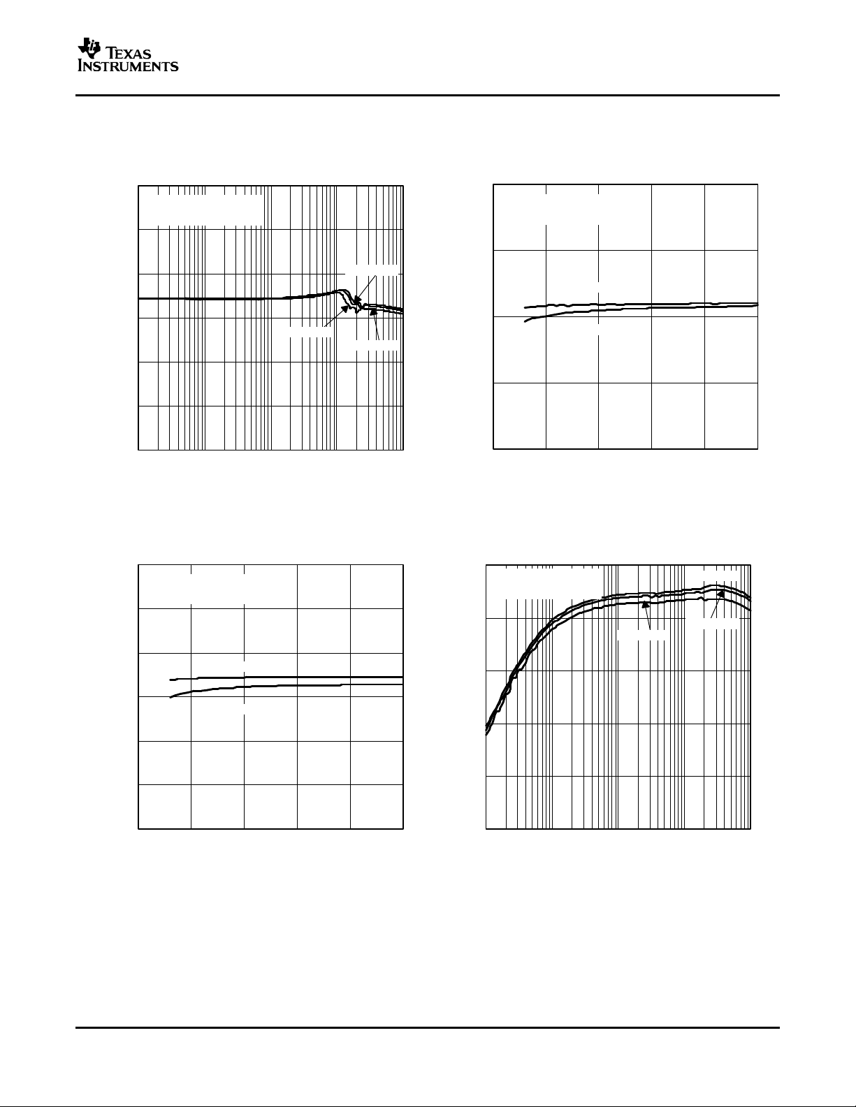
TYPICAL CHARACTERISTICS (continued)
SWITCHING FREQUENCY (SLOW) SWITCHING FREQUENCY (MED)
vs vs
OUTPUT CURRENT OUTPUT CURRENT
Figure 9.
(2)
Figure 10.
SWITCHING FREQUENCY (FAST) 1.05-V OUTPUT VOLTAGE
vs vs
OUTPUT CURRENT OUTPUT CURRENT
Figure 11. Figure 12.
(2) The data of Figure 9 –Figure 12 are measured from the Typical Application Circuit of Figure 25 and Table 2 .
12
Page 13
www.ti.com
1.425
1.450
1.475
1.500
1.525
1.550
1.575
0.001 0.01 0.1 1 10
VI = 21 V
VI = 12 V
VI = 7 V
1.5 V
TONSEL = FLOA T
V
OUT2
− Output Voltage − V
I
OUT2
− Output Current − A
1
1.025
1.050
1.075
1.1
0 5 10 15 20 25
1.05 V
TONSEL = FLOA T
V
OUT1
− Output Voltage − V
VI − Input Voltage − V
IO = 0 A
IO = 5 A
1.425
1.450
1.475
1.500
1.525
1.550
1.575
0 5 10 15 20 25
1.5 V
TONSEL = FLOA T
V
OUT2
− Output Voltage − V
VI − Input Voltage − V
IO = 0 A
IO = 5 A
0
20
40
60
80
100
0.001 0.01 0.1 1 10
VI= 21 V
VI= 7 V
1.05 V
TONSEL = FLOAT
I
OUT1
− Output Current − A
VI= 12 V
− Efficiency − %
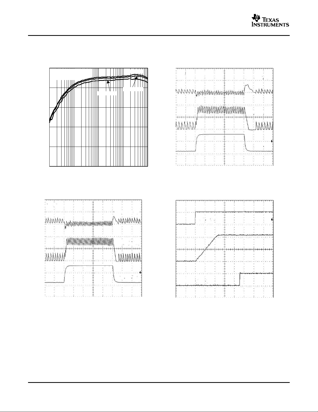
TYPICAL CHARACTERISTICS (continued)
TPS51124
SLVS616A – NOVEMBER 2005 – REVISED NOVEMBER 2005
1.5-V OUTPUT VOLTAGE 1.05-V OUTPUT VOLTAGE
vs vs
OUTPUT CURRENT INPUT VOLTAGE
Figure 13.
(3)
1.5-V OUTPUT VOLTAGE 1.05-V EFFICIENCY
vs vs
INPUT VOLTAGE OUTPUT CURRENT
Figure 14.
(3) The data of Figure 13 –Figure 16 are measured from the Typical Application Circuit of Figure 25 and Table 2
Figure 15. Figure 16.
13
Page 14
www.ti.com
TONSEL = FLOAT
V
OUT1
(50 mV/div)
IIND1 (5 A/div)
I
OUT1
(5 A/div)
t − Time − 20 s/div
0
20
40
60
80
100
0.001 0.01 0.1 1 10
VI= 21 V
VI= 7 V
1.5 V
TONSEL = FLOAT
I
OUT2
− Output Current − A
VI= 12 V
− Efficiency − %
TONSEL = FLOAT
V
OUT2
(50 mV/div)
IIND2 (5 A/div)
I
OUT2
(5 A/div)
t − Time − 20 s/div
t − Time − 500 s/div
EN1 (5 V/div)
VO1 (0.5 V/div)
PGOOD1 (5 V/div)
TPS51124
SLVS616A – NOVEMBER 2005 – REVISED NOVEMBER 2005
TYPICAL CHARACTERISTICS (continued)
1.5-V EFFICIENCY 1.05-V LOAD TRANSIENT RESPONSE
vs
OUTPUT CURRENT
Figure 17.
(4)
1.5-V LOAD TRANSIENT RESPONSE 1.05-V START-UP WAVEFORMS
Figure 18.
(4) The data of Figure 17 –Figure 20 are measured from the Typical Application Circuit of Figure 25 and Table 2
Figure 19. Figure 20.
14
Page 15
www.ti.com
t − Time − 500 s/div
EN2 (5 V/div)
VO2 (0.5 V/div)
PGOOD2 (5 V/div)
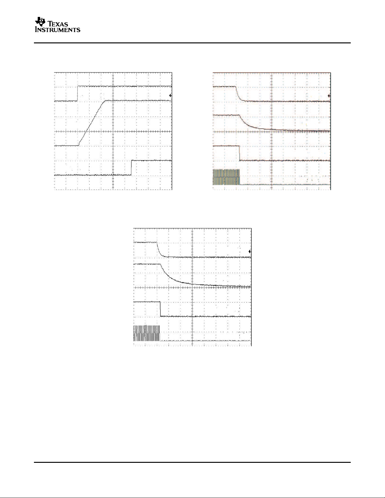
t Time −1 ms/div−
EN1
(5 V/div)
VO1 (1 V/div)
PGOOD1 (5 V/div)
DRVL1 (5 V/div)
t − Time − 1 ms/div
EN2 (5 V/div)
VO2 (1 V/div)
PGOOD2 (5 V/div)
DRVL2 (5 V/div)
SLVS616A – NOVEMBER 2005 – REVISED NOVEMBER 2005
TYPICAL CHARACTERISTICS (continued)
1.5-V START-UP WAVEFORMS 1.05-V DISCHARGE WAVEFORMS
TPS51124
Figure 21.
(5)
Figure 22.
1.5-V DISCHARGE WAVEFORMS
Figure 23.
(5) The data of Figure 21 –Figure 23 are measured from the Typical Application Circuit of Figure 25 and Table 2
15
Page 16
www.ti.com
ESR
R1
Co
+
0.758V
R2
Control
Logic
And
Driver
RL
VIN
VFB
DRVH
DRVL
PWM
Switching Modulator
Voltage Divider
Vc
Output Capacitor
Lx
I
L
I
C
I
O
−
+
ƒ
o
1
2 ESR Co
ƒ
sw
4
Vripple
Vout
0.758
10 [mV]
TPS51124
SLVS616A – NOVEMBER 2005 – REVISED NOVEMBER 2005
APPLICATION INFORMATION
LOOP COMPENSATION AND EXTERNAL PARTS SELECTION
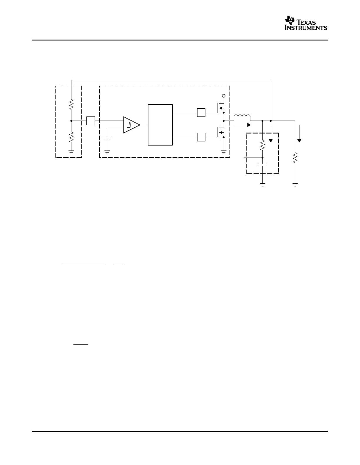
A buck converter system using D-CAP Mode can be simplified as shown below.
Figure 24. Simplifying the Modulator
The output voltage is compared with an internal reference voltage after divider resistors, R1 and R2. The PWM
comparator determines the timing to turn on the high-side MOSFET. The gain and speed of the comparator is
high enough to keep the voltage at the beginning of each on cycle (or the end of off cycle) substantially constant.
The DC output voltage may have line regulation due to ripple amplitude that slightly increases as the input
voltage increase.
For the loop stability, the 0-dB frequency, f0, defined in Equation 4 needs to be lower than 1/4 of the switching
frequency.
As f0is determined solely by the output capacitor’s characteristics, loop stability of D-CAP Mode is determined by
the capacitor’s chemistry. For example, specialty polymer capacitors (SP-CAP) have Co in the order of several
100 µ F and ESR in range of 10 m Ω . These make f0in the order of 100 kHz or less and the loop is stable.
However, ceramic capacitors have f0at more than 700 kHz, which is not suitable for this operational mode.
Although D-CAP Mode provides many advantages such as ease-of-use, minimum external components
configuration, and extremely short response time, a sufficient amount of feedback signal needs to be provided by
an external circuit to reduce jitter level. This is due to not employing an error amplifier in the loop. The required
signal level is approximately 10 mV at the comparing point (VFB terminal). This gives Vripple at the output node
as shown in the following equation.
The output capacitor's ESR should meet this requirement.
(4)
(5)
16
Page 17

www.ti.com
R1
V
out
0.758
0.758
R2
L
1
I
IND(ripple)
ƒ
V
IN(max)
V
OUT
V
OUT
V
IN(max)
3
I
OUT(max)
ƒ
V
IN(max)
V
OUT
V
OUT
V
IN(max)
I
IND(peak)
V
trip
R
DS(on)
1
L ƒ
V
IN(max)
V
OUT
V
OUT
V
IN(max)
ESR
V
OUT
0.01
I
ripple
V
OUT
I
OUT(max)
30 [m]
SLVS616A – NOVEMBER 2005 – REVISED NOVEMBER 2005
APPLICATION INFORMATION (continued)
The external components selection is much simpler in D-CAP Mode.
1. Determine the value of R1 and R2.
Recommended R2 value is from 10 k Ω to 100 k Ω . Determine R1 using the following equation.
2. Choose inductor.
The inductance value should be determined to give the ripple current of approximately 1/4 to 1/2 of maximum
output current. Larger ripple current increases the output ripple voltage, improves S/N ratio, and contributes
to a stable operation.
The inductor also needs to have low DCR to achieve good efficiency, as well as enough room above peak
inductor current before saturation. The peak inductor current can be estimated as follows.
TPS51124
(6)
(7)
3. Choose output capacitor(s).
Organic semiconductor capacitor(s) or specialty polymer capacitor(s) are recommended. Determine ESR to
meet the required ripple voltage indicated previously. A quick approximation is shown here:
LAYOUT CONSIDERATIONS
Certain points must be considered before starting a layout using the TPS51124.
• Connect RC low-pass filter from V5IN to V5FILT, 1- µ F and 3.3- Ω are recommended. Place the filter
capacitor close to the IC, within 12 mm (0.5 inch) if possible.
• Connect the over-current setting resistors from TRIPx to GND, and as close as possible to the IC. The trace
from TRIPx to resistor, and resistor to GND, should avoid coupling to high-voltage switching node.
• The discharge path (VOx) should have a dedicated trace to the output capacitor(s), separate from the output
voltage sensing trace. Use 1,5-mm (60 mils) or wider trace, with no loops. Tie the feedback-current-setting
resistor (the resistor between VFBx to GND) close to the IC’s GND. The trace from this resistor to VFBx pin
should be short and thin. Place on the component side and avoid vias between this resistor and the IC.
• Connections from the drivers to the respective gate of the high-side or the low-side MOSFET should be as
short as possible to reduce stray inductance. Use 0,65-mm (25 mils) or wider trace.
• All sensitive analog traces and components such as VOx, VFBx, GND, ENx, PGOODx, TRIPx, V5FILT, and
TONSEL should be placed away from high-voltage switching nodes such as LLx, DRVLx, DRVHx, or VBSTx
nodes to avoid coupling. Use internal layer(s) as ground plane(s) and shield the feedback trace from power
traces and components.
• Gather ground terminal of VIN capacitor(s), Vout capacitor(s), and source of low-side MOSFETs as close as
possible. GND (signal ground) and PGNDx (power ground) should be connected strongly together near the
IC. PCB trace defined as LLx node, which connects to source of high-side MOSFET, drain of low-side
MOSFET and high-voltage side of the inductor, should be as short and wide as possible.
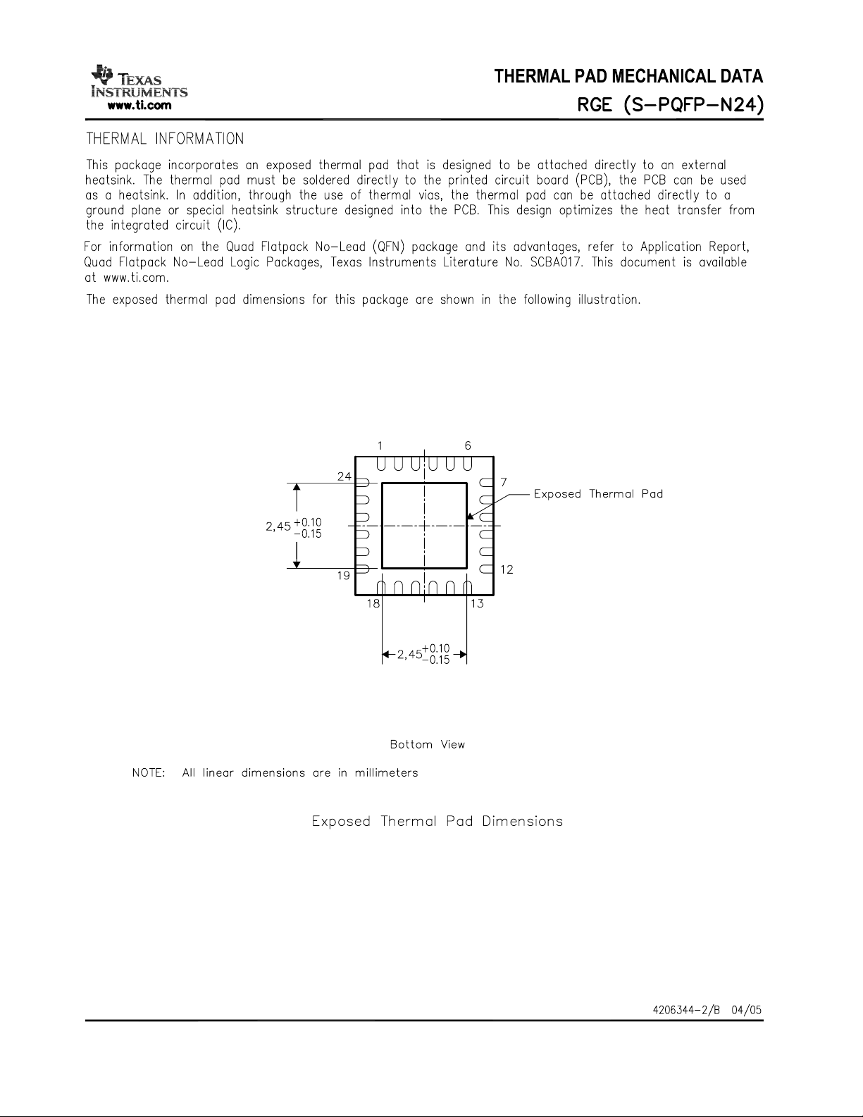
• In order to effectively remove heat from the package, prepare thermal land and solder to the package’s
thermal pad ( PowerPAD™). Two by two or more vias with a 0,33-mm (13 mils) diameter connected from the
thermal land to the internal ground plane should be used to help dissipation. Do NOT connect PGNDx to this
thermal land underneath the package.
(8)
(9)
17
Page 18
www.ti.com
75 kΩ
9
10
11
12
PGOOD1
EN1
PGOOD2
EN2
TPS51124RGE
(QFN24)
13 14 15 16
VBST1
DRVL1
LL1
DRVH1
VBST2
DRVH2
LL2
DRVL2
17
8
7
6 5 4 3 2 1
18
19
20
21
22
23
24
VO1
1.05 V/10 A
Q2
IRF8113
L1
Q1
IRF7821
VO2
1.5 V/10 A
Q4
IRF8113
L2
Q3
IRF7821
Input Voltage
3 V to 28 V
PowerPAD
TM
C7
R6
C3
C1
C6
C4
R3
6.8
C8
R7
R1
R2
75
R5
R4
V5IN
4.5 V to 5.5 V
VO2
VO1
VFB2
TONSEL
GND
VFB1
PGND2
TRIP2
V5FILT
V5IN
TRIP1
PGND1
Power
Good2
EN2
C5
C2
Power
Good1
EN1
SGND
PGNDPGND
SGND
C9
SGND PGND
PGND
73.2 kΩ
kΩ
28.7 kΩ
22 µF
2 x 330 µF
1 µH
10 µF
0.1 µF
4.7 μF
6.8 kΩ
1 μF
3.3Ω
kΩ
0.1 µF
10 µF
1 µH
2 x 330 µF
TPS51124
SLVS616A – NOVEMBER 2005 – REVISED NOVEMBER 2005
APPLICATION INFORMATION (continued)
18
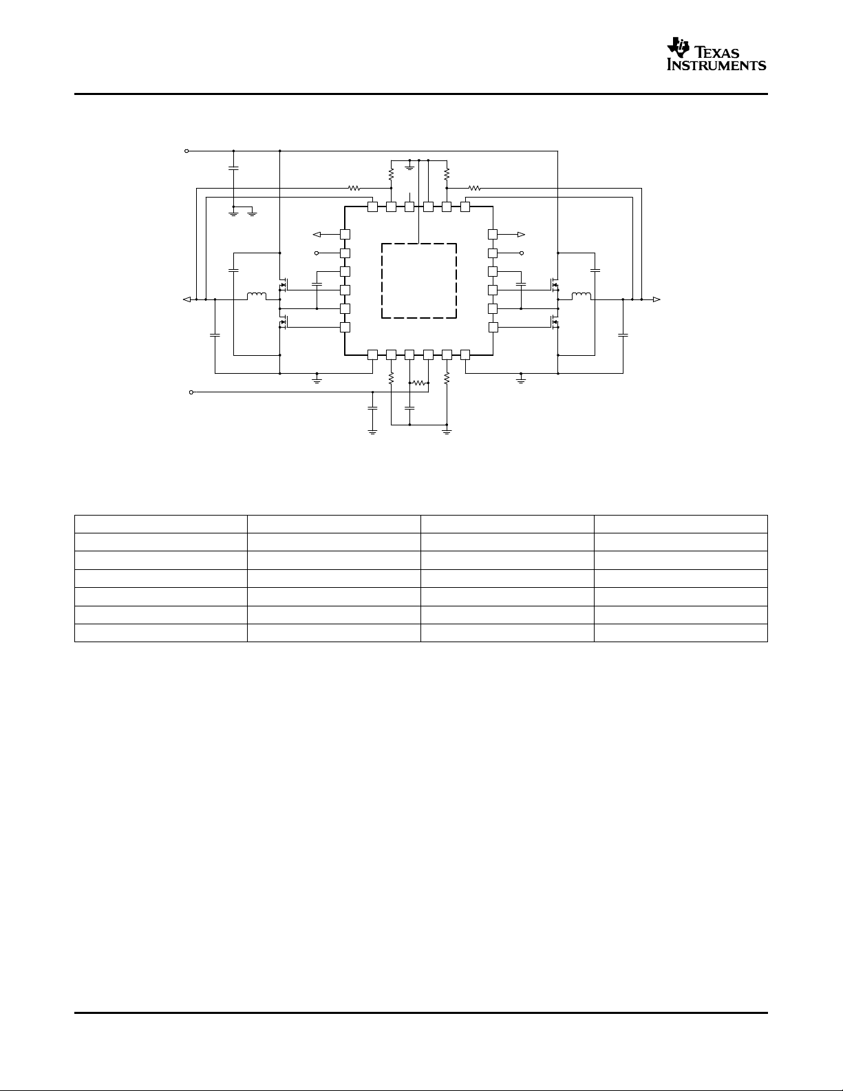
Figure 25. Typical Application Circuit
Table 2. Typical Application Circuit Components
SYMBOL SPECIFICATION MANUFACTURER PART NUMBER
C1 330 µ F, 2.5 V, 15 m Ω SANYO 2R5TPE330MF
C4 330 µ F, 2.5 V, 18 m Ω SANYO 2R5TPE330MI
L1, L2 1 µ H, 2 m Ω TOKO FDA1254-1R0M
C3, C6 10 µ F, 25 V TDK C3225X5R1E106
Q1, Q3 30 V, 13 m Ω International Rectifier IRF7821
Q2, Q4 30 V, 7 m Ω International Rectifier IRF8113
Page 19

PACKAGE OPTION ADDENDUM
www.ti.com
27-Feb-2006
PACKAGING INFORMATION
Orderable Device Status
(1)
Package
Type
Package
Drawing
Pins Package
Qty
Eco Plan
TPS51124RGER ACTIVE QFN RGE 24 3000 Green (RoHS &
no Sb/Br)
TPS51124RGERG4 ACTIVE QFN RGE 24 3000 Green (RoHS &
no Sb/Br)
TPS51124RGET ACTIVE QFN RGE 24 250 Green (RoHS &
no Sb/Br)
TPS51124RGETG4 ACTIVE QFN RGE 24 250 Green (RoHS &
no Sb/Br)
(1)
The marketing status values are defined as follows:
ACTIVE: Product device recommended for new designs.
LIFEBUY: TI has announced that the device will be discontinued, and a lifetime-buy period is in effect.
NRND: Not recommended for new designs. Device is in production to support existing customers, but TI does not recommend using this part in
a new design.
PREVIEW: Device has been announced but is not in production. Samples may or may not be available.
OBSOLETE: TI has discontinued the production of the device.
(2)
Eco Plan - The planned eco-friendly classification: Pb-Free (RoHS), Pb-Free (RoHS Exempt), or Green (RoHS & no Sb/Br) - please check
http://www.ti.com/productcontent for the latest availability information and additional product content details.
TBD: The Pb-Free/Green conversion plan has not been defined.
Pb-Free (RoHS): TI's terms "Lead-Free" or "Pb-Free" mean semiconductor products that are compatible with the current RoHS requirements
for all 6 substances, including the requirement that lead not exceed 0.1% by weight in homogeneous materials. Where designed to be soldered
at high temperatures, TI Pb-Free products are suitable for use in specified lead-free processes.
Pb-Free (RoHS Exempt): This component has a RoHS exemption for either 1) lead-based flip-chip solder bumps used between the die and
package, or 2) lead-based die adhesive used between the die and leadframe. The component is otherwise considered Pb-Free (RoHS
compatible) as defined above.
Green (RoHS & no Sb/Br): TI defines "Green" to mean Pb-Free (RoHS compatible), and free of Bromine (Br) and Antimony (Sb) based flame
retardants (Br or Sb do not exceed 0.1% by weight in homogeneous material)
(2)
Lead/Ball Finish MSL Peak Temp
CU NIPDAU Level-2-260C-1 YEAR
CU NIPDAU Level-2-260C-1 YEAR
CU NIPDAU Level-2-260C-1 YEAR
CU NIPDAU Level-2-260C-1 YEAR
(3)
(3)
MSL, Peak Temp. -- The Moisture Sensitivity Level rating according to the JEDEC industry standard classifications, and peak solder
temperature.
Important Information and Disclaimer:The information provided on this page represents TI's knowledge and belief as of the date that it is
provided. TI bases its knowledge and belief on information provided by third parties, and makes no representation or warranty as to the
accuracy of such information. Efforts are underway to better integrate information from third parties. TI has taken and continues to take
reasonable steps to provide representative and accurate information but may not have conducted destructive testing or chemical analysis on
incoming materials and chemicals. TI and TI suppliers consider certain information to be proprietary, and thus CAS numbers and other limited
information may not be available for release.
In no event shall TI's liability arising out of such information exceed the total purchase price of the TI part(s) at issue in this document sold by TI
to Customer on an annual basis.
Addendum-Page 1
Page 20
Page 21
Page 22

IMPORTANT NOTICE
Texas Instruments Incorporated and its subsidiaries (TI) reserve the right to make corrections, modifications,
enhancements, improvements, and other changes to its products and services at any time and to discontinue
any product or service without notice. Customers should obtain the latest relevant information before placing
orders and should verify that such information is current and complete. All products are sold subject to TI’s terms
and conditions of sale supplied at the time of order acknowledgment.
TI warrants performance of its hardware products to the specifications applicable at the time of sale in
accordance with TI’s standard warranty. Testing and other quality control techniques are used to the extent TI
deems necessary to support this warranty. Except where mandated by government requirements, testing of all
parameters of each product is not necessarily performed.
TI assumes no liability for applications assistance or customer product design. Customers are responsible for
their products and applications using TI components. To minimize the risks associated with customer products
and applications, customers should provide adequate design and operating safeguards.
TI does not warrant or represent that any license, either express or implied, is granted under any TI patent right,
copyright, mask work right, or other TI intellectual property right relating to any combination, machine, or process
in which TI products or services are used. Information published by TI regarding third-party products or services
does not constitute a license from TI to use such products or services or a warranty or endorsement thereof.
Use of such information may require a license from a third party under the patents or other intellectual property
of the third party, or a license from TI under the patents or other intellectual property of TI.
Reproduction of information in TI data books or data sheets is permissible only if reproduction is without
alteration and is accompanied by all associated warranties, conditions, limitations, and notices. Reproduction
of this information with alteration is an unfair and deceptive business practice. TI is not responsible or liable for
such altered documentation.
Resale of TI products or services with statements different from or beyond the parameters stated by TI for that
product or service voids all express and any implied warranties for the associated TI product or service and
is an unfair and deceptive business practice. TI is not responsible or liable for any such statements.
Following are URLs where you can obtain information on other Texas Instruments products and application
solutions:
Products Applications
Amplifiers amplifier.ti.com Audio www.ti.com/audio
Data Converters dataconverter.ti.com Automotive www.ti.com/automotive
DSP dsp.ti.com Broadband www.ti.com/broadband
Interface interface.ti.com Digital Control www.ti.com/digitalcontrol
Logic logic.ti.com Military www.ti.com/military
Power Mgmt power.ti.com Optical Networking www.ti.com/opticalnetwork
Microcontrollers microcontroller.ti.com Security www.ti.com/security
Telephony www.ti.com/telephony
Video & Imaging www.ti.com/video
Wireless www.ti.com/wireless
Mailing Address: Texas Instruments
Post Office Box 655303 Dallas, Texas 75265
Copyright 2006, Texas Instruments Incorporated
Loading...