

Page 1

INTEGRATED CIRCUITS
TPM754A
Microcontroller with TrackPoint
microcode from IBM
Preliminary specification
Replaces datasheet TPM754 of 1997 Dec 03
IC28 Data Handbook
1999 Nov 11
Page 2
Philips Semiconductors Preliminary specification
TPM754AMicrocontroller with TrackPoint microcode from IBM
The Philips Semiconductors TPM754 is a small package, low cost,
ROM-coded 80C51 with IBM’s TrackPoint pointing algorithms
and control code. TrackPoint is the result of years of human factors
research and innovation at IBM. The result is a “velocity sensitive”
pointing solution more efficient and easier to use than “position
sensitive” devices such as the mouse, the trackball, or the touchpad.
IBM has licensed Philips Semiconductors to sell microcontrollers
with TrackPoint code. By purchasing a TPM from Philips, the
purchaser becomes a sub-licensee of Philips. The selling price of
Philips’ TPM includes the royalties for IBM’s intellectual property,
which Philips in turn pays to IBM. Customers for TPMs do not need
to sign any licensing agreement with either IBM or Philips. This code
is the intellectual property of IBM, which is covered by numerous
patents, and must be treated accordingly.
The TPM754 contains IBM TrackPoint code, a single module
PCA, a 256 × 8 RAM, 21 I/O lines, two 16-bit counter/timers, a
two-priority level interrupt structure, a full duplex serial channel, an
on-chip oscillator, and an 8-bit D/A converter.
For identical device without TrackPoint code, see the 8XC754
datasheet.
FEA TURES
•80C51-based architecture
•Small package sizes – 28-pin SSOP
•Power control modes:
– Idle mode
– Power-down mode
•256 × 8 RAM
•Two 16-bit auto reloadable counter/timers
•Single module PCA counter/timer
•Full duplex serial channel
•Boolean processor
•CMOS and TTL compatible
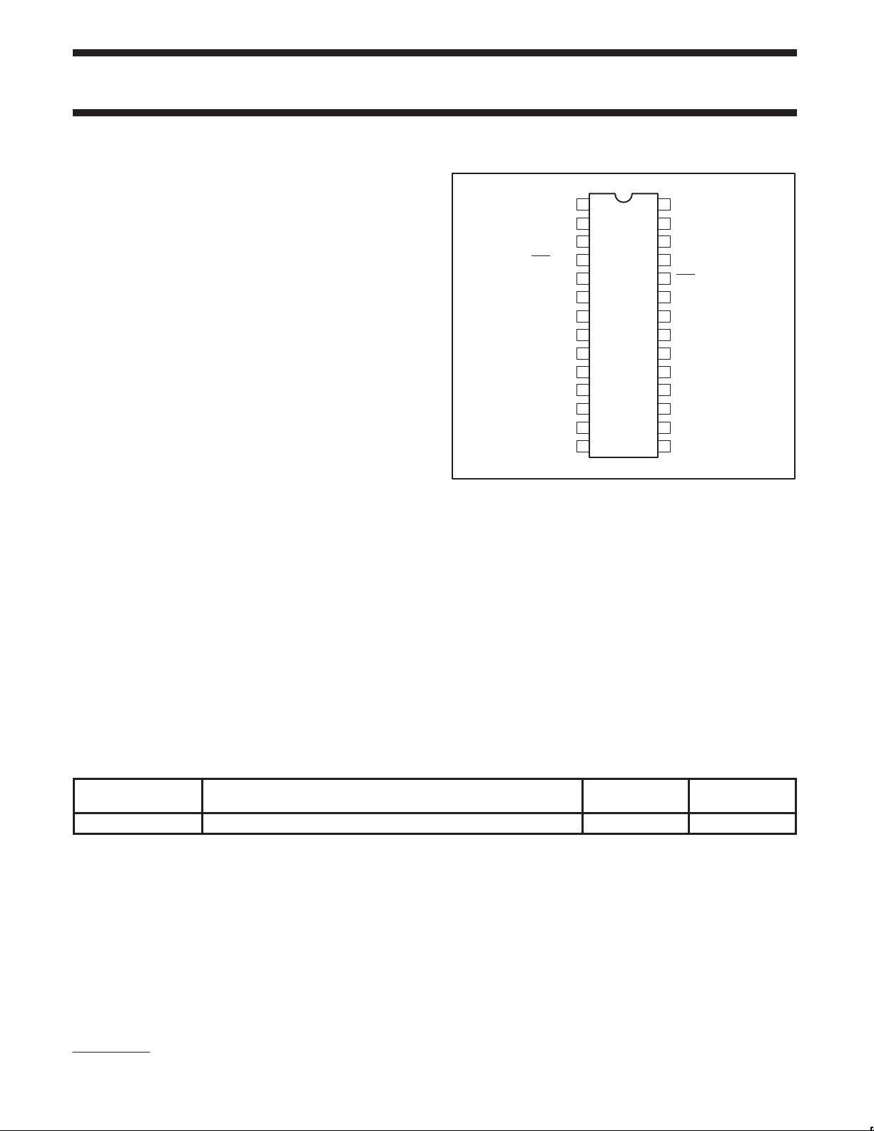
PIN CONFIGURATION
1
TxD/T1/P3.5
ECI/P3.6
INT1
2
3
4
/P3.7
5
RST
6
X2
7
X1
8
V
SS
9
ZIN
10
YIN
11
XIN
12 17
13 16 VREGAV
SS
14 15 DECOUPLEAV
CC
PLASTIC
SHRINK
SMALL
OUTLINE
PACKAGE
28RxD/T0/P3.4
P3.3
27
P3.2
26
P3.1
25
P3.0
24
INT0
23
CEX/P1.1
22
V
21
P1.2
20
XYDAC
19
ZDAC/ASEL
18
XYSOURCE
XYDACBIASXYZRAMP
/P1.0
CC
SU00726B
ORDERING INFORMA TION
ORDERING CODE
PTPM754A DB 0 to +70, 28-pin Shrink Small Outline Package 3.5 to 12 MHz SOT341-1
NOTE:
1. PTPM754A has improved start-up from low-voltage power down.
IBM is a registered trademark, and TrackPoint is a trademark of IBM Corporation.
1999 Nov 1 1
TEMPERATURE RANGE °C
AND PACKAGE
2
FREQUENCY
DRAWING
NUMBER
Page 3

Philips Semiconductors Preliminary specification
TPM754AMicrocontroller with TrackPoint microcode from IBM
PIN DESCRIPTION
MNEMONIC DIP
PIN NO.
V
SS
V
CC
22 I Supply voltage during normal, idle, and power-down operation.
P1.0–P1.2 21, 23, 24 I/O Port 1: Port 1 is a 3-bit bidirectional I/O port with internal pull-ups on P1.0 and P1.1. Port 1 pins that
24 I INT0 (P1.0): External interrupt 0.
23 O CEX (P1.1): PCA clock output.
P3.0–P3.7 1–4,
25–28
RST 5 I Reset: A high on this pin for two machine cycles while the oscillator is running resets the device.
X1 7 I Crystal 1: Input to the inverting oscillator amplifier and input to the internal clock generator circuits.
X2 6 O Crystal 2: Output from the inverting oscillator amplifier.
AV
AV
CC
SS
1
1
14 I Analog supply voltage and reference input.
13 I Analog supply and reference ground.
ZIN 9 I ZIN: Input to analog multiplexer.
YIN 10 I YIN: Input to analog multiplexer.
XIN 11 I XIN: Input to analog multiplexer.
XYZRAMP 12 O XYZRAMP: Provides a low impedance pulldown to VSS under S/W control.
DECOUPLE 15 O DECOUPLE: Output from regulated supply for connection of decoupling capacitors.
VREG 16 O VREG: Provides regulated analog supply output.
XYDACBIAS 17 O XYDACBIAS: Provides source voltage for bias of external circuitry.
XYSOURCE 18 O XYSOURCE: Provides source voltage from regulated analog supply.
ZDAC 19 O ZDAC: Switchable output from the internal DAC.
XYDAC 20 O XYDAC: Non-switchable output from the internal DAC.
NOTE:
1. AV
(reference ground) must be connected to 0 V (ground). AVCC (reference input) cannot differ from VCC by more than ±0.2 V, and must
SS
be in the range 4.5 V to 5.5 V .
TYPE NAME AND FUNCTION
8 I Circuit Ground Potential.
have 1s written to them can be used as inputs. As inputs, port 1 pins that are externally pulled low will
source current because of the internal pull-ups (P1.0, P1.1). (See DC Electrical Characteristics: I
Port 1 also serves the special function features listed below (Note: P1.0 does not have the strong
pullup that is on for 2 oscillator periods.):
I/O Port 3: Port 3 is an 8-bit bidirectional I/O port with internal pull-ups. Port 3 pins that have 1s written to
them are pulled high by the internal pull-ups and can be used as inputs. As inputs, port 3 pins that are
externally being pulled low will source current because of the pull-ups. (See DC Electrical
Characteristics: I
). (Note: P3.5 does not have the strong pullup that is on for 2 oscillator periods.)
IL
Port 3 also serves the special function as listed below:
3 I ECI (P3.6): External PCA clock input.
1 I RxD/T0 (P3.4): Serial port receiver data input.
Timer 0 external clock input.
4 I INT1: External interrupt 1.
2 I TxD/T1 (P3.5): Serial port transmitter data.
Timer 1 external clock input.
(NOTE: The TPM754 does not have an internal reset resistor.)
).
IL
1999 Nov 1 1
3
Page 4

Philips Semiconductors Preliminary specification
TPM754AMicrocontroller with TrackPoint microcode from IBM
OSCILLA T OR CHARACTERISTICS
X1 and X2 are the input and output, respectively, of an inverting
amplifier which can be configured for use as an on-chip oscillator.
To drive the device from an external clock source, X1 should be
driven while X2 is left unconnected. There are no requirements on
the duty cycle of the external clock signal, because the input to the
internal clock circuitry is through a divide-by-two flip-flop. However,
minimum and maximum high and low times specified in the data
sheet must be observed.
IDLE MODE
The TPM754 includes the 80C51 power-down and idle mode
features. In idle mode, the CPU puts itself to sleep while all of the
on-chip peripherals except the D/A stays active. The functions that
continue to run while in the idle mode are the timers and the
interrupts. The instruction to invoke the idle mode is the last
instruction executed in the normal operating mode before the idle
mode is activated. The CPU contents, the on-chip RAM, and all of
the special function registers remain intact during this mode. The
idle mode can be terminated either by any enabled interrupt (at
which time the process is picked up at the interrupt service routine
and continued), or by a hardware reset which starts the processor in
the same manner as a power-on reset. Upon powering-up the
circuit, or exiting from idle mode, sufficient time must be allowed for
stabilization of the internal analog reference voltages before a D/A
conversion is started.
I/O Ports
The I/O pins provided by the TPM754 consist of port 1 and port 3.
Port 1
Port 1 is a 3-bit bidirectional I/O port and includes alternate functions
on some pins of this port. Pins P1.0 and P1.1 are provided with
internal pullups while the remaining pin (P1.2) has an open drain
output structure. The alternate functions for port 1 are:
INT0
– External interrupt 0.
CEX – PCA clock output.
Port 3
Port 3 is an 8-bit bidirectional I/O port structure.
The alternate functions for port 3 are:
RxD – Serial port receiver data input.
T1 – Timer 1 external clock input.
– External interrupt 1.
INT1
TxD – Serial port transmitter data.
T0 – Timer 0 external clock input.
ECI – PCA external clock input.
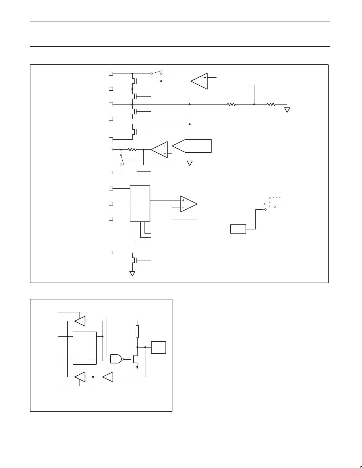
Analog Section
The analog section of the TPM754, shown in Figure 1, consists of
four major elements: a bandgap referenced voltage regulator, an
8-bit DAC, an input multiplexer and comparator, and a low
impedance pulldown device.
The bandgap voltage regulator uses the AV
produces a regulated output on the VREG pin. The regulator also
supplies the analog supply voltage for the DAC. The regulator may
be switched on/off by means of the AC1 bit in the analog control
register (ACON0). The regulator output may also be supplied to the
XYDACBIAS and XYSOURCE pins by means of bits AC3 and AC4,
respectively. The DECOUPLE pin is provided for decoupling the
regulator output.
pin as its supply and
CC
The DAC is an 8-bit device and its output appears on the XYDAC
pin. In addition, the DAC output may also be routed to the ZDAC pin
by means of bit AC6 in the ACON0 register. The DAC output is not
buffered, so external load impedances should be taken into
consideration when using either of these outputs.
A 3-input multiplexer is provided, whose output is connected to the
positive reference of a comparator. The multiplexer output is
controlled by bits MUX2:0 of ACON1. A bandgap reference supplies
the negative reference of the comparator. The output of the
comparator may be used the trigger the capture input of module 4 of
the PCA.
A low impedance pulldown is supplied at the XYZRAMP pin and is
controlled by bit AC5 of ACON0.
The functions of the analog section are controlled by the IBM
TrackPoint code embedded within the Philips TPM754.
PC BOARD LAYOUT CONSIDERATIONS
The TrackPoint is a low-level analog circuit. While not difficult to
implement, careful consideration should be given to circuit board
layout to obtain proper operation of the TrackPoint. The
considerations are similar to that used for radio frequency
application. The circuit should be located far from the CPU and
video lines, and should also be shielded from any digital signals. A
100µV pulse picked up every 3 or 4 seconds is sufficient to cause
cursor drift. A good circuit board layout will result in a circuit that is
very stable and will hold the cursor on a pixel for days at a time.
However, the autorouters of most software board layout packages
will not do an adequate job, and manual routing of this portion of the
motherboard is recommended.
The TPM754 has excellent supply regulation for the analog portions
of the TrackPoint circuit. However , care should be taken with respect
to the circuit ground to avoid voltage shifts due to non-TrackPoint
loads. The analog part of the circuit must have its own ground
plane, isolated from everything else and connected to the main
ground at just one point (no ground loops). All of the analog portion
of the TrackPoint circuit, and nothing else, must be over this
ground island.
No digital traces can pass though the analog area on any level from
the ground plane out. The circuit should be confined to one side of
the ground plane, preferably on the first interior layer, with the
ground plane next. The circuit should be powered only at a single
point (pin 14), and that power should be filtered to ground before it
comes onto the analog area.
The signal lines from the TrackPoint sensor stick can be sensitive to
pickup, and should be run close together, and not too close to digital
lines. A grounded guard trace is a good idea. Most important, the
stick common line is not a ground line, but rather a signal line,
although it will eventually connect to the analog ground. A common
and serious error is to treat it as ground, connecting it to a general
ground at some convenient point.
The layout should be designed to keep things compact and minimize
trace lengths. The whole circuit, analog and digital, will fit
comfortably within 2cm × 3cm. In some situations, it may be
desirable to put the circuit on a separate card instead of on the
motherboard. In this case, a shielded cable should provide the best
means of connecting the stick signals to the circuit card.
1999 Nov 1 1
4
Page 5
Philips Semiconductors Preliminary specification
TPM754AMicrocontroller with TrackPoint microcode from IBM
AV
DECOUPLE
VREG
XYDACBIAS
XYSOURCE
XYDAC
CC
1K
AC1
AC2
AC3
AC4
DCON 7:0 (84H)
BANDGAP REF*
20K 10K
*ENABLED/DISABLED BY AC0
READ
LATCH
INT. BUS
DQ
ZDAC
ZIN
YIN
XIN
XYZRAMP
ALTERNATE
OUTPUT
FUNCTION
ANALOG
MUX
V
DD
AC6
MUX0
MUX1
MUX2
AC5
Figure 1. Analog Section
INTERNAL*
PULL-UP
AC7
TO PCA TRIGGER
BANDGAP REF
EXT
SU00765A
LATCH
WRITE TO
LATCH
READ
PIN
*PINS LISTED AS OPEN DRAIN WILL NOT HAVE THIS PULLUP
CL Q
ALTERNATE INPUT
FUNCTION
Figure 2. Typical Port Bit Latches and I/O Buffers
1999 Nov 1 1
PIN
SU00671
5
Page 6

Philips Semiconductors Preliminary specification
SYMBOL
PARAMETER
TEST CONDITIONS
UNIT
TPM754AMicrocontroller with TrackPoint microcode from IBM
ABSOLUTE MAXIMUM RATINGS
PARAMETER
1, 3, 4
RATING UNIT
Storage temperature range –65 to +150 °C
Voltage from V
Voltage from any pin to V
CC
to V
SS
SS
–0.5 to +6.5 V
–0.5 to VCC + 0.5 V
Power dissipation 1.0 W
DC ELECTRICAL CHARACTERISTICS
T
= 0°C to +70°C, AVCC = 5 V ±5, AVSS = 0 V
amb
VCC = 5 V ± 10%, VSS = 0 V
I
CC
Supply current (see Figure 5)
Inputs
V
IL
V
IH
V
IH1
Input low voltage, port 1, 3 –0.5
Input high voltage, port 1, 3 0.2VCC+0.9 VCC+0.5 V
Input high voltage, X1, RST 0.7V
Outputs
V
OL
V
OL1
V
OH
I
LI
C
IO
Output low voltage, port 3, 1.2 IOL = 1.6 mA
Output low voltage, port 1.0, 1.1 IOL = 3.2 mA
Output high voltage, ports 3, 1.0, 1.1 IOH = –60 µA, 2.4 V
Input leakage current, port 1, 3, RST 0.45 < VIN < V
Pin capacitance Test freq = 1 MHz,
NOTES:
1. Stresses above those listed under Absolute Maximum Ratings may cause permanent damage to the device. This is a stress rating only and
functional operation of the device at these or any conditions other than those described in the AC and DC Electrical Characteristics section
of this specification is not implied.
2. Under steady state (non-transient) conditions, IOL must be externally limited as follows:
Maximum I
Maximum I
Maximum total I
If I
exceeds the test condition, VOL may exceed the related specification. Pins are not guaranteed to sink current greater than the listed
OL
test conditions.
per port pin: 10mA
OL
per 8-bit port: 26mA
OL
for all outputs: 67mA
OL
3. This product includes circuitry specifically designed for the protection of its internal devices from the damaging effects of excessive static
charge. Nonetheless, it is suggested that conventional precautions be taken to avoid applying greater than the rated maxima.
4. Parameters are valid over operating temperature range unless otherwise specified. All voltages are with respect to V
noted.
5. Power-down I
6. I
is measured with all output pins disconnected; X1 driven with t
CC
RST = V
7. Idle I
is measured with all output pins disconnected; X1 driven with t
CC
RST = V
8. Pin 9, 10, 11, and 21; V
is measured with all output pins disconnected; X2, X1 n.c.; RST = VSS.
CC
. ICC will be slightly higher if a crystal oscillator is used.
CC
.
SS
≤ V
REG
.
IN
4
4
LIMITS
MIN TYP
CC
2
2
CC
1
MAX
0.2VCC–0.1
VCC+0.5 V
0.45 V
0.45 V
±10 µA
V
10 pF
T
= 25°C
amb
unless otherwise
SS
, t
CLCH
= 5 ns, VIL = VSS + 0.5 V, VIH = VCC – 0.5 V; X2 n.c.;
CHCL
, t
CLCH
= 5 ns, VIL = VSS + 0.5 V, VIH = VCC – 0.5 V; X2 n.c.;
CHCL
1999 Nov 1 1
6
Page 7
Philips Semiconductors Preliminary specification
SYMBOL
PARAMETER
TEST CONDITIONS
UNIT
TPM754AMicrocontroller with TrackPoint microcode from IBM
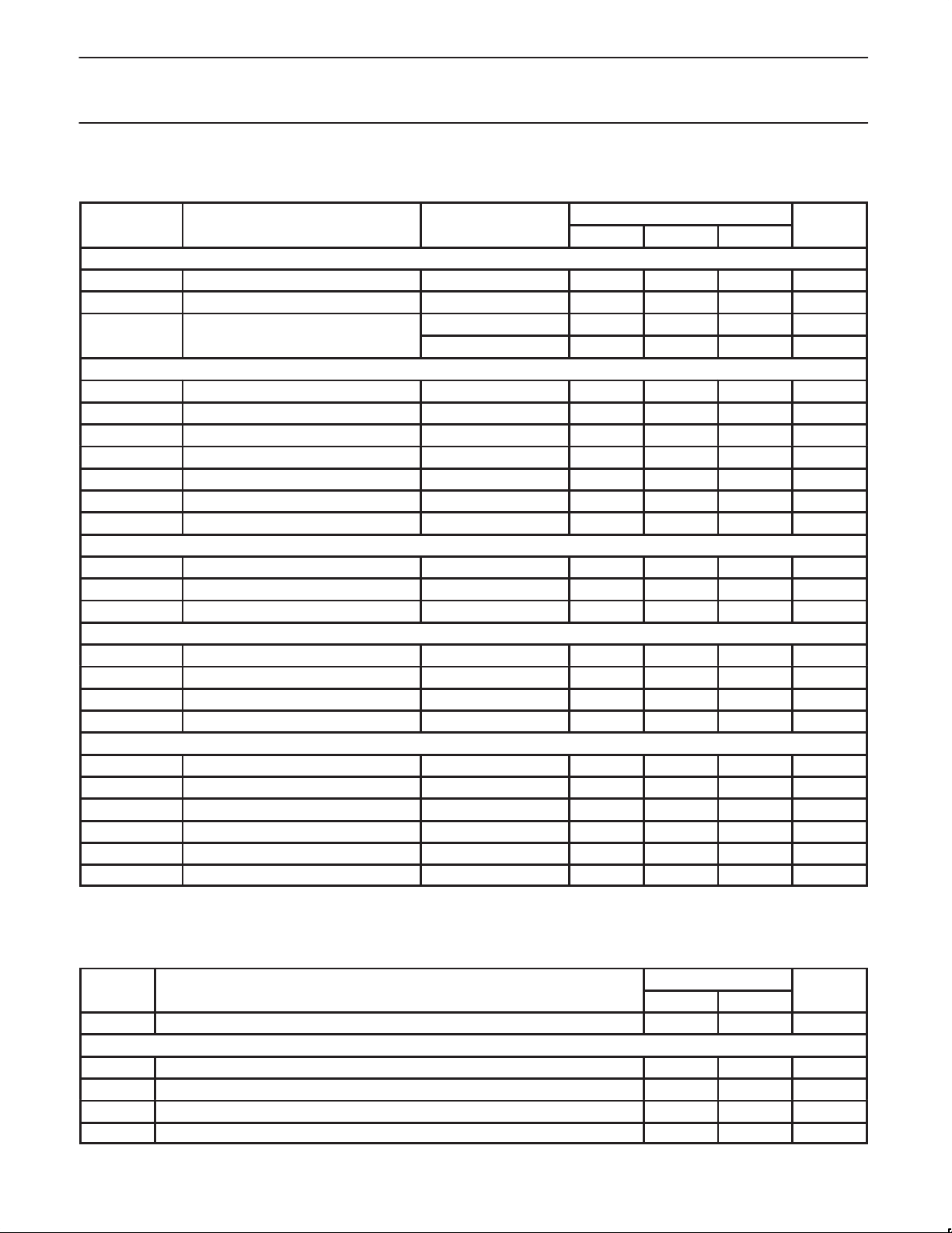
ANALOG SECTION ELECTRICAL CHARACTERISTICS
T
= 0°C to +70°C; VCC = 5 V ± 10%, VSS = 0 V
amb
MIN TYP
Analog Inputs
AV
CC
Analog supply voltage 4.5 – 5.5 V
Sensor resistor 330 – 3K Ω
IAV
CC
AC0 = 0 IC only – 1.2 2.5 mA
AC0 = 1 – – 10 µA
Regulator
VREG IVREG = 13 mA 3.6 3.8 4.3 V
ICHARGE Decouple current C
= 10 µF – 60 100 mA
DEC
CDECOUPLE Stability requirement – 10 – µF
RDSONQ1 – 7 12 Ω
ILEAKAGEQ1 –10 +10 µA
ILEAKAGEQ2 –10 +10 µA
PSRR 100 Hz – –40 – dB
MUX and Comparator
Comparator trip point 1.14 1.26 1.38 V
MUX impedance – 1 4 kΩ
ILEAKAGEMUX VIN ≤ V
REG
–10 +10 µA
Digital-to-Analog Conversion
ZDAC, XYDAC monotonicity 8 – – bits
ZDAC switch impedance – 75 200 Ω
DAC output resistance – 2.7 5 kΩ
ZDAC switch leakage –10 +10 µA
Switches
XYZRAMP impedance – 33 100 Ω
XYZRAMP leakage –10 +10 µA
XYDACBIAS impedance – 13 25 Ω
XYDACBIAS leakage –10 +10 µA
XYSOURCE impedance – 200 400 Ω
XYSOURCE leakage –10 +70 µA
LIMITS
4
1
MAX
AC ELECTRICAL CHARACTERISTICS
T
= 0°C to +70°C, VCC = 5 V ±10%, VSS = 0 V
amb
SYMBOL PARAMETER MIN MAX UNIT
1/t
CLCL
External Clock (Figure 3)
t
CHCX
t
CLCX
t
CLCH
t
CHCL
1999 Nov 1 1
4
VARIABLE CLOCK
Oscillator frequency: 3.5 12 MHz
High time 20 ns
Low time 20 ns
Rise time 20 ns
Fall time 20 ns
7
Page 8
Philips Semiconductors Preliminary specification
TPM754AMicrocontroller with TrackPoint microcode from IBM
EXPLANATION OF THE AC SYMBOLS
Each timing symbol has five characters. The first character is always
‘t’ (= time). The other characters, depending on their positions,
indicate the name of a signal or the logical status of that signal.
The designations are:
C – Clock
D – Input data
H – Logic level high
L – Logic level low
Q – Output data
T – Time
V – Valid
X – No longer a valid logic level
Z – Float
VCC –0.5
0.45V
V
CC
0.45V
–0.5
t
t
CHCL
CLCX
t
CLCL
t
CLCH
t
CHCX
SU00297
0.2 V
0.2 V
+ 0.9
CC
– 0.1
CC
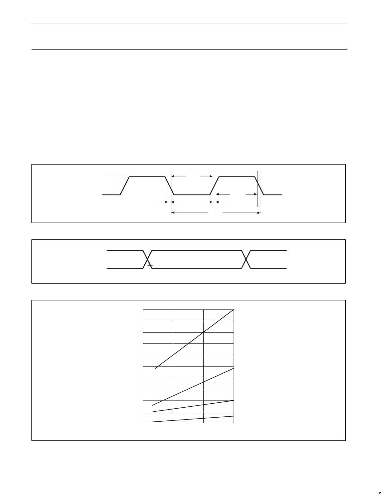
Figure 3. External Clock Drive
0.2 VCC + 0.9
0.2 VCC – 0.1
SU00307
Figure 4. AC Testing Input/Output
20
18
16
14
12
I
mA
CC
10
8
MAX ACTIVE I
TYP ACTIVE I
CC
CC
6
6
1999 Nov 1 1
Maximum I
6
4
2
4MHz 8MHz 12MHz
FREQ
MAX IDLE I
TYP IDLE I
Figure 5. ICC vs. FREQ
values taken at VCC = 5.5V and worst case temperature.
CC
Typical I
values taken at VCC = 5.0V and 25°C.
CC
Notes 6 and 7 refer to AC Electrical Characteristics.
8
7
CC
7
CC
SU00739
Page 9
1999 Nov 1 1
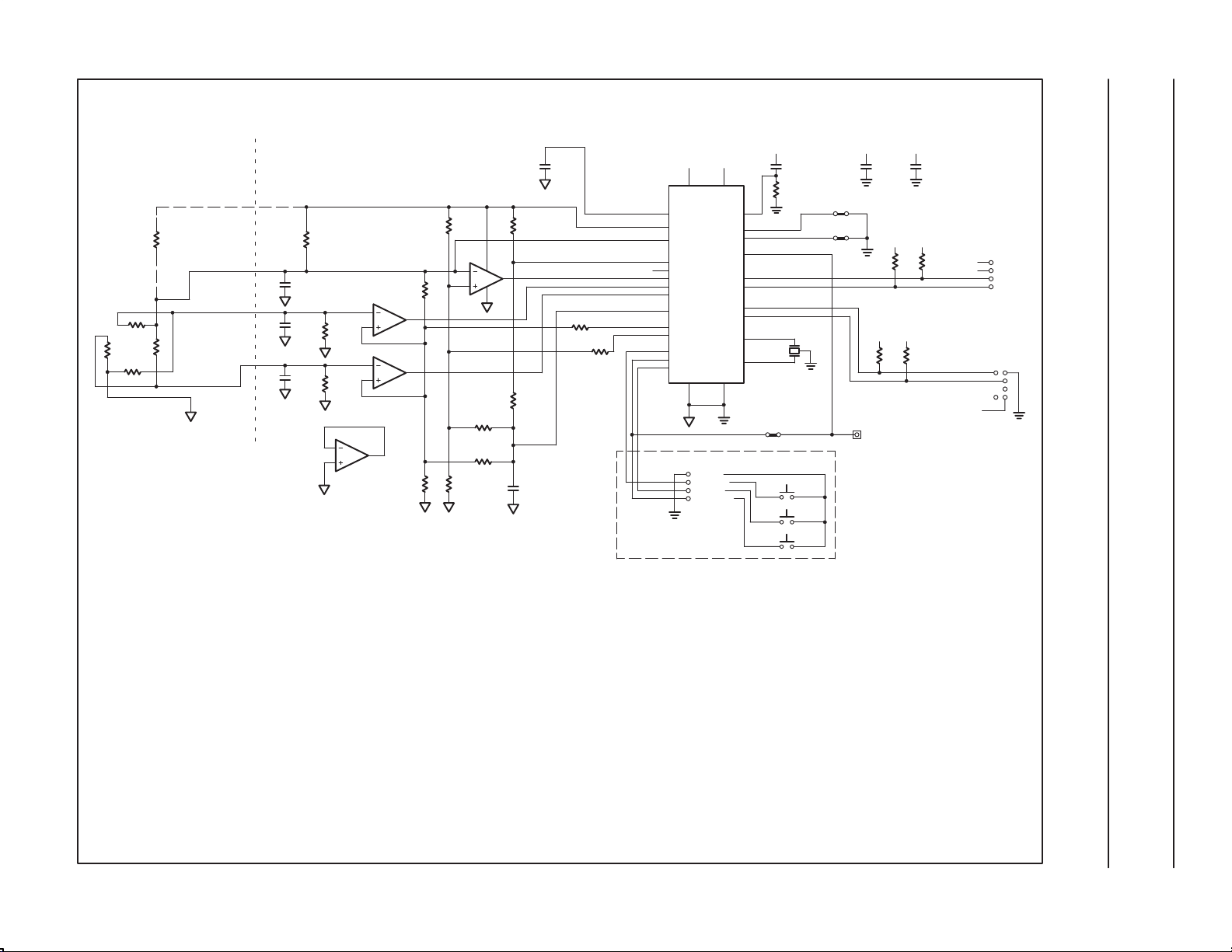
SCHEMATIC OF TRACKPOINT SYSTEM
Philips Semiconductors Preliminary specification
+5
RST
P3.6
P3.3
P1.1
INT0
INT1
X2
X1
+
5
3
INVERT Y
28
INVERT Z
23
TACTILE
24
2
4
1
6
X1
12.0MHz
7
JMP1
SEE NOTE 3
1
1
1
C4
2.2uF
R8
100K
5%
RIGHT
2
LEFT
2
MIDDLE
2
SEE NOTE 8
SEE NOTE 9
+
FORCE SENSOR
C1
+
SEE NOTE 10
X
SEE NOTE 10
R1
Z or +
C6
0.01uF
Y
C7
0.01uF
C8
0.01uF
R23
R24
+Y
+X
–X
–Y
X
LMC6036
6
U2
5
LMC6036
9
U2
10
R16
2
3
R4
LMC6036
7
8
COMMON
STICK WIRING MAY VARY
TYPICAL WIRING SHOWN FOR
REFERENCE ONLY
9
LMC6036
13
14
U2
12
R17
R5
R18
4
U2
11
R9
R15
1
R11
C2
0.01uF
10% OR BETTER
TEMPERATURE STABLE
R7
R6
MID
+5
14 22
AVCC VCC
U1
TPM754
15
DEC
16
VREG
17
XYDB
18
XYS
21
WIN
9
ZIN
10
YIN
11
XIN
12
RMP
20
XYD
19
ZDAC
26
P3.1
27
P3.2
25
P3.0
AVSS VSS
13
BUTTONS
BUTTON ASSEMBLY
COM
1
RIGHT
2
LEFT
3
MIDDLE
4
+5
TXD/T1
RXD/T0
8
+5
JMP2
JMP3
+5
+
R10
10K
5%
C5
10uF
+5
+5
R2
R3
4.7K
4.7K
5%
5%
+5
R14
10K
5%
CLK
DATA
C3
0.1uF
+5
TACTILE FEEDBACK OUTPUT
CN1
TO SYSTEM BOARD
COM
GND
1
VCC
+5
2
CLK
3
DATA
4
MOUSE
6 PIN MINI DIN
5
3
1
2
4
6
+5
NOTES:
1. All resistors 1% low noise unless noted.
2. Middle button switch is optional.
3. Jumper JMP1 is only installed when middle button is not present, otherwise it is not populated.
4. Connectors are shown for reference only.
5. Connection between analog and digital ground must be a single point connection close to the TPM754.
6. Component values that are not specified depend upon stick sensitivity, geometry, impedance, and tolerance.
7. TPM754 Reset pin (Pin 5) can be driven by system power on reset signal (active High). Omit C4, R 8 in this case.
8. If Pin 3 is grounded, positive voltage swing on the stick’s Y terminal will move the cursor downward (–Y), otherwise upward.
9. If Pin 28 is grounded, positive voltage swing on the stick’s terminal will be interpreted as downward (–Z) force, otherwise upward.
10. A Z axis series resistor and a fifth stick terminal may be present.
11. For most current information, see www.ibm.com.
TPM754AMicrocontroller with TrackPoint microcode from IBM
TYPCIAL TARGET SETTINGS
SU00815F
50 counts per Z DAC step
18 counts per XY DAC step
3.2 grams/count XY
10 grams/count Z
Page 10
Philips Semiconductors Preliminary specification
TPM754AMicrocontroller with TrackPoint microcode from IBM
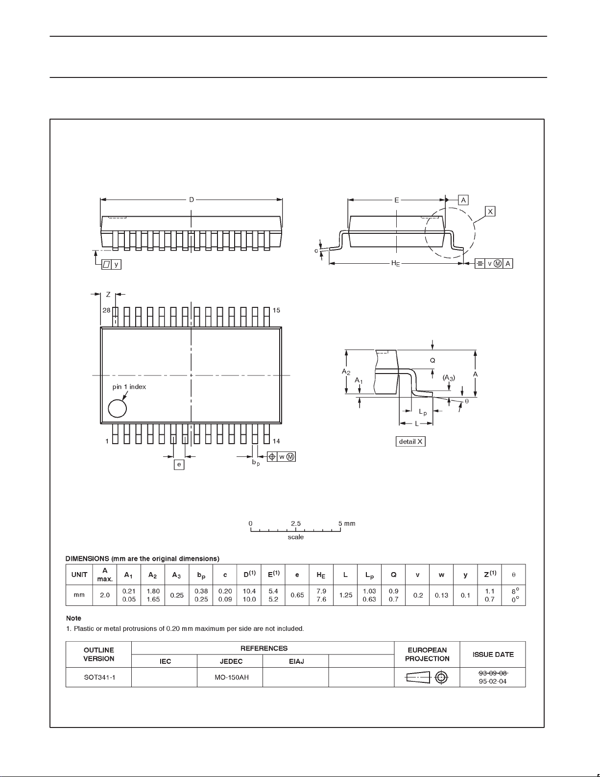
SSOP28: plastic shrink small outline package; 28 leads; body width 5.3mm SOT341-1
1999 Nov 1 1
10
Page 11

Philips Semiconductors Preliminary specification
TPM754AMicrocontroller with TrackPoint microcode from IBM
NOTES
1999 Nov 1 1
11
Page 12

Philips Semiconductors Preliminary specification
TPM754AMicrocontroller with TrackPoint microcode from IBM
Data sheet status
Data sheet
status
Objective
specification
Preliminary
specification
Product
specification
Product
status
Development
Qualification
Production
Definition
This data sheet contains the design target or goal specifications for product development.
Specification may change in any manner without notice.
This data sheet contains preliminary data, and supplementary data will be published at a later date.
Philips Semiconductors reserves the right to make changes at any time without notice in order to
improve design and supply the best possible product.
This data sheet contains final specifications. Philips Semiconductors reserves the right to make
changes at any time without notice in order to improve design and supply the best possible product.
[1]
[1] Please consult the most recently issued datasheet before initiating or completing a design.
Definitions
Short-form specification — The data in a short-form specification is extracted from a full data sheet with the same type number and title. For
detailed information see the relevant data sheet or data handbook.
Limiting values definition — Limiting values given are in accordance with the Absolute Maximum Rating System (IEC 134). Stress above one
or more of the limiting values may cause permanent damage to the device. These are stress ratings only and operation of the device at these or
at any other conditions above those given in the Characteristics sections of the specification is not implied. Exposure to limiting values for extended
periods may affect device reliability.
Application information — Applications that are described herein for any of these products are for illustrative purposes only. Philips
Semiconductors make no representation or warranty that such applications will be suitable for the specified use without further testing or
modification.
Disclaimers
Life support — These products are not designed for use in life support appliances, devices or systems where malfunction of these products can
reasonably be expected to result in personal injury . Philips Semiconductors customers using or selling these products for use in such applications
do so at their own risk and agree to fully indemnify Philips Semiconductors for any damages resulting from such application.
Right to make changes — Philips Semiconductors reserves the right to make changes, without notice, in the products, including circuits, standard
cells, and/or software, described or contained herein in order to improve design and/or performance. Philips Semiconductors assumes no
responsibility or liability for the use of any of these products, conveys no license or title under any patent, copyright, or mask work right to these
products, and makes no representations or warranties that these products are free from patent, copyright, or mask work right infringement, unless
otherwise specified.
Philips Semiconductors
811 East Arques Avenue
P.O. Box 3409
Sunnyvale, California 94088–3409
Telephone 800-234-7381
Copyright Philips Electronics North America Corporation 1998
All rights reserved. Printed in U.S.A.
Date of release: 11-99
Document order number: 9397 750 06577
1999 Nov 1 1
12
 Loading...