

Page 1

TPM749
Microcontroller with TrackPoint
microcode from IBM
Product specification 1996 May 01
INTEGRATED CIRCUITS
Data Handbook IC20
Page 2
Philips Semiconductors Product specification
TPM749Microcontroller with TrackPoint microcode from IBM
2
1996 May 01 853-1831 16753
DESCRIPTION
The Philips Semiconductors TPM749 is a small package, low cost,
ROM-coded 80C51 with IBM’s TrackPoint pointing algorithms
and control code. TrackPoint is the result of years of human factors
research and innovation at IBM. The result is a “velocity sensitive”
pointing solution more efficient and easier to use than “position
sensitive” devices such as the mouse, the trackball, or the touchpad.
IBM has licensed Philips Semiconductors to sell microcontrollers
with TrackPoint code. By purchasing a TPM from Philips, the
purchaser becomes a sub-licensee of Philips. The selling price of
Philips’ TPM includes the royalties for IBM’s intellectual property,
which Philips in turn pays to IBM. Customers for TPMs do not need
to sign any licensing agreement with either IBM or Philips. This code
is the intellectual property of IBM, which is covered by numerous
patents, and must be treated accordingly.
The TPM is fabricated with Philips high-density CMOS technology.
Philips epitaxial substrate minimizes CMOS latch-up sensitivity.
The TPM contains a 2k × 8 ROM, a 64 × 8 RAM, 21 I/O lines, a
16-bit auto-reload counter/timer, a fixed-priority level interrupt
structure, an on-chip oscillator, a five channel multiplexed 8-bit A/D
converter, and an 8-bit PWM output.
The TPM supports two power reduction modes of operation referred
to as the idle mode and the power-down mode.
FEATURES
•80C51 based architecture
•Small package sizes
– 28-pin Shrink Small Outline Package (SSOP)
– 28-pin PLCC
•Low power consumption:
– Normal operation: less than 11mA @ 5V, 12MHz
– Idle mode
– Power-down mode
•2k × 8 ROM
•64 × 8 RAM
•16-bit auto reloadable counter/timer
•5-channel 8-bit A/D converter
•8-bit PWM output/timer
•10-bit fixed-rate timer
•CMOS and TTL compatible
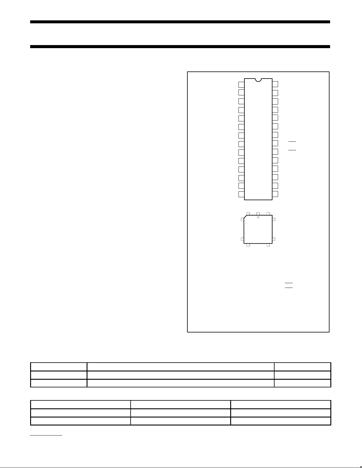
PIN CONFIGURATION
1
2
3
4
5
6
7
8
9
10
11
12
14
13
15
16
17
18
19
20
21
22
23
24
P3.4/A4
P3.3/A3
P3.2/A2/A10
P3.1/A1/A9
P3.0/A0/A8
P0.2
RST
X2
X1
V
SS
P0.0/ASEL
P1.4/ADC4/D4
AV
SS
AV
CC
P1.5/INT0/D5
P1.6/INT1
/D6
P1.7/T0/D7
P0.3
P0.4/PWM OUT
P3.7/A7
P3.6/A6
P3.5/A5
V
CC
SHRINK
SMALL
OUTLINE
PACKAGE
PLASTIC
LEADED
CHIP
CARRIER
4 1 26
5
11
25
19
12 18
P0.1/OE
25
26
27
28
P1.0/ADC0/D0
P1.1/ADC1/D1
P1.3/ADC3/D3
P1.2/ADC2/D2
Pin Function
1 P3.4/A4
2 P3.3/A3
3 P3.2/A2/A10
4 P3.1/A1/A9
5 P3.0/A0/A8
6 P0.2
7 P0.1/OE
8 P0.0/ASEL
9 RST
10 X2
11 X1
12 V
SS
13 P1.0/ADC0/D0
14 P1.1/ADC1/D1
Pin Function
15 P1.2/ADC2/D2
16 P1.3/ADC3/D3
17 P1.4/ADC4/D4
18 AV
SS
19 AV
CC
20 P1.5/INT0/D5
21 P1.6/INT1
/D6
22 P1.7/T0/D7
23 P0.3
24 P0.4/PWM OUT
25 P3.7/A7
26 P3.6/A6
27 P3.5/A5
28 V
CC
SU00692A
ORDERING INFORMATION
ORDERING CODE TEMPERATURE RANGE AND PACKAGE DRAWING NUMBER
PTPM749 A 0 to +70°C, Plastic Leaded Chip Carrier SOT261-3
PTPM749 DB 0 to +70°C, Shrink Small Ouline Package SOT341-1
For compatible pointing device, contact:
COMPANY
CONTACT TELEPHONE
Bokam Engineering Ms. Jane Kamenster (714)513-2200
CTS Corporation Mr. Dave Poole (219)589-7169
IBM is a registered trademark, and TrackPoint is a trademark of IBM Corporation.
Page 3

Philips Semiconductors Product specification
TPM749Microcontroller with TrackPoint microcode from IBM
1996 May 01
3
PIN DESCRIPTION
MNEMONIC PIN NO. TYPE NAME AND FUNCTION
V
SS
12 I Circuit Ground Potential.
V
CC
28 I Supply voltage during normal, idle, and power-down operation.
P0.0–P0.4 8–6
23, 24
I/O Port 0: Port 0 is a 5-bit bidirectional port. Port 0.0–P0.2 are open drain. Port 0.0–P0.2 pins that have
1s written to them float, and in that state can be used as high-impedance inputs. P0.3–P0.4 are
bidirectional I/O port pins with internal pull-ups. These pins are driven low if the port register bit is
written with a 0. The state of the pin can always be read from the port register by the program. Port 0.3
and 0.4 have internal pull-ups that function identically to port 3. Pins that have 1s written to them are
pulled high by the internal pull-ups and can be used as inputs.
While P0.0 anbd P0.1 differ from “standard TTL” characteristics, they are close enough for the pins to
still be used as general-purpose I/O.
6 I VPP (P0.2) – Programming voltage input.
7 I OE (P0.1) – Input which specifies verify mode (output enable).
OE = 1 output enabled (verify mode).
8 I ASEL (P0.0) – Input which indicates which bits of the EPROM address are applied to port 3.
ASEL = 0 low address byte available on port 3.
ASEL = 1 high address byte available on port 3 (only the three least significant bits are used).
P1.0–P1.7 13–17,
20–22
I/O Port 1: Port 1 is an 8-bit bidirectional I/O port with internal pull-ups. Port 1 pins that have 1s written to
them are pulled high by the internal pull-ups and can be used as inputs. P0.3–P0.4 pins are
bidirectional I/O port pins with internal pull-ups. As inputs, port 1 pins that are externally pulled low will
source current because of the internal pull-ups. (See DC Electrical Characteristics: I
IL
). Port 1 also
serves the special function features of the SC80C51 family as listed below:
20 I INT0 (P1.5): External interrupt.
21 I INT1 (P1.6): External interrupt.
22 I T0 (P1.7): Timer 0 external input.
13–17 I ADC0 (P1.0)–ADC4 (P1.4): Port 1 also functions as the inputs to the five channel multiplexed A/D
converter. These pins can be used as outputs only if the A/D function has been disabled. These pins
can be used as digital inputs while the A/D converter is enabled.
Port 1 serves to output the addressed EPROM contents in the verify mode and accepts as inputs the
value to program into the selected address during the program mode.
P3.0–P3.7 5–1,
27–25
I/O Port 3: Port 3 is an 8-bit bidirectional I/O port with internal pull-ups. Port 3 pins that have 1s written to
them are pulled high by the internal pull-ups and can be used as inputs. As inputs, port 3 pins that are
externally being pulled low will source current because of the pull-ups. (See DC Electrical
Characteristics: IIL). Port 3 also functions as the address input for the EPROM memory location to be
programmed (or verified). The 11-bit address is multiplexed into this port as specified by P0.0/ASEL.
RST 9 I Reset: A high on this pin for two machine cycles while the oscillator is running resets the device. An
internal diffused resistor to V
SS
permits a power-on RESET using only an external capacitor to VCC.
After the device is reset, a 10-bit serial sequence, sent LSB first, applied to RESET, places the device
in the programming state allowing programming address, data and V
PP
to be applied for programming
or verification purposes. The RESET serial sequence must be synchronized with the X1 input.
X1 11 I Crystal 1: Input to the inverting oscillator amplifier and input to the internal clock generator circuits. X1
also serves as the clock to strobe in a serial bit stream into RESET to place the device in the
programming state.
X2 10 O Crystal 2: Output from the inverting oscillator amplifier.
AV
CC
1
19 I Analog supply voltage and reference input.
AV
SS
1
18 I Analog supply and reference ground.
NOTE:
1. AV
SS
(reference ground) must be connected to 0V (ground). AVCC (reference input) cannot differ from VCC by more than ±0.2V, and must be
in the range 4.5V to 5.5V.
Page 4
Philips Semiconductors Product specification
TPM749Microcontroller with TrackPoint microcode from IBM
1996 May 01
4
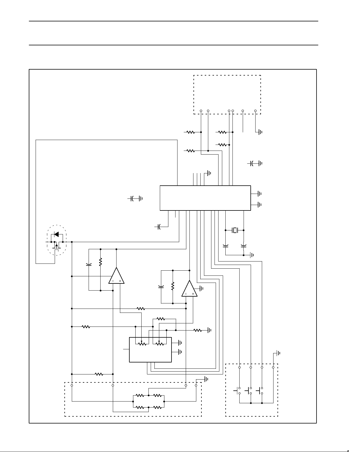
SCHEMATIC OF TrackPoint SYSTEM WITH PHILIPS TPM749
9
281913
17
21222326252410
11
RST
VCC
AVCC
ADC0
ADC4
P1.6
P1.7
P0.3
P3.6
P3.7
P0.4
X2
X1
P3.3
P3.5
P3.2
P3.4
2273
1
FTRANS
BUTTON3 *
INVERTX *
NOTMOU
8
P0.0
P0.17P3.0
P3.1
5
4
R1
10K
+5
R3
10K
+5
R9
6.04K
+5
R10
6.04K
+5
CLK
DATA
MCLK
MDATA
+5
GND
+5
PTPM749
U2
PLCC28
P1.5
20
C4
10uF
+5
+
TO EXTERNAL
MOUSE
TO
SYSTEM
BOARD
VSS
12
AVSS
18
X1
12.0MHz
C2
33pFC133pF
MIDDLE
LEFT
RIGHT
BUTTON ASSEMBLY
C7
0.1uF
+5
C3
2.2uF
+5
+
+5
LMC6482
1
2
3
4
U1
R6
650K *
C5
33pF
LMC6482
7
6
5
8
U1
R2
650K *
C6
33pF
+5
2
3
Q1
VP0610T
1
R8
1M
R5
332
R1
10K
R0
10K
VB
1
GND
8
R4
10K
3
54121311
976
DATA
CLK
RST
VCC
16
+5
U3
DS1267-10
R11
10K
R7
1M
Y+
Y–
X+
X–
PS1
PSTICK
STICK ASSEMBLY
1. CONNECT BUTTON 3 SIGNAL TO GND IF MIDDLE BUTTON USED.
2. CONNECT INVERTX SIGNAL TO GND IF BOKAM SENSOR USED.
3. Q1 MAY BE REPLACED WITH A JUMPER IF POWER DRAW IS NOT A CONCERN.
C5, C6 MAY THEN BE INCREASED TO A MAXIMUM OF 3900pF.
4. R9, R10 MAY BE INCREASED IF CABLE TO SYSTEM BOARD IS SHORT.
5. +5V, GND CONNECTIONS TO SYSTEM SUPPLY SHOULD BE FROM A SINGLE POINT CONNECTION.
6. THIS CIRCUIT CAN ONLY BE USED WHEN OVERALL STICK RESISTANCE HAS PRODUCTION VARIATIONS WITHIN 5%.
SU00694
MANUFACTURER:
Q1 – SILICONIX
U3 – DALLAS SEMICONDUCTOR
Page 5
Philips Semiconductors Product specification
TPM749Microcontroller with TrackPoint microcode from IBM
1996 May 01
5
OSCILLATOR CHARACTERISTICS
X1 and X2 are the input and output, respectively, of an inverting
amplifier which can be configured for use as an on-chip oscillator.
To drive the device from an external clock source, X1 should be
driven while X2 is left unconnected. There are no requirements on
the duty cycle of the external clock signal, because the input to the
internal clock circuitry is through a divide-by-two flip-flop. However,
minimum and maximum high and low times specified in the data
sheet must be observed.
IDLE MODE
The TPM includes the 80C51 power-down and idle mode features.
In idle mode, the CPU puts itself to sleep while all of the on-chip
peripherals except the A/D and PWM stay active. The functions that
continue to run while in the idle mode are Timer 0, Timer I, and the
interrupts. The instruction to invoke the idle mode is the last
instruction executed in the normal operating mode before the idle
mode is activated. The CPU contents, the on-chip RAM, and all of
the special function registers remain intact during this mode. The
idle mode can be terminated either by any enabled interrupt (at
which time the process is picked up at the interrupt service routine
and continued), or by a hardware reset which starts the processor in
the same manner as a power-on reset. Upon powering-up the
circuit, or exiting from idle mode, sufficient time must be allowed for
stabilization of the internal analog reference voltages before an A/D
conversion is started.
POWER-DOWN MODE
In the power-down mode, the oscillator is stopped and the
instruction to invoke power-down is the last instruction executed.
Only the contents of the on-chip RAM are preserved. A hardware
reset is the only way to terminate the power-down mode. The control
bits for the reduced power modes are in the special function register
PCON.
Table 1. External Pin Status During Idle and
Power-Down Modes
MODE Port 0* Port 1 Port 2
Idle Data Data Data
Power-down Data Data Data
* Except for PWM output (P0.4).
I/O Ports
The I/O pins provided by the TPM consist of port 0, port 1, and
port 3.
Port 0
Port 0 is a 5-bit bidirectional I/O port and includes alternate functions
on some pins of this port. Pins P0.3 and P0.4 are provided with
internal pullups while the remaining pins (P0.0, P0.1, and P0.2) have
open drain output structures. The alternate function for port P0.4 is
PWM output.
If the alternate function PWM is not being used, then this pin may be
used as an I/O port.
Port 1
Port 1 is an 8-bit bidirectional I/O port whose structure is identical to
the 80C51, but also includes alternate input functions on all pins.
The alternate pin functions for port 1 are:
P1.0-P1.4 - ADC0-ADC4 - A/D converter analog inputs
P1.5 INT0
- external interrupt 0 input
P1.6 INT1
- external interrupt 1 input
P1.7 - T0 - timer 0 external input
If the alternate functions INT0
, INT1, or T0 are not being used, these
pins may be used as standard I/O ports. It is necessary to connect
AV
CC
and AVSS to VCC and VSS, respectively, in order to use P1.5,
P1.6, and P1.7 pins as standard I/O pins. When the A/D converter is
enabled, the analog channel connected to the A/D may not be used
as a digital input; however, the remaining analog inputs may be used
as digital inputs. They may not be used as digital outputs. While the
A/D is enabled, the analog inputs are floating.
Port 3
Port 3 is an 8-bit bidirectional I/O port whose structure is identical to
the 80C51. Note that the alternate functions associated with port 3
of the 80C51 have been moved to port 1 of the TPM (as applicable).
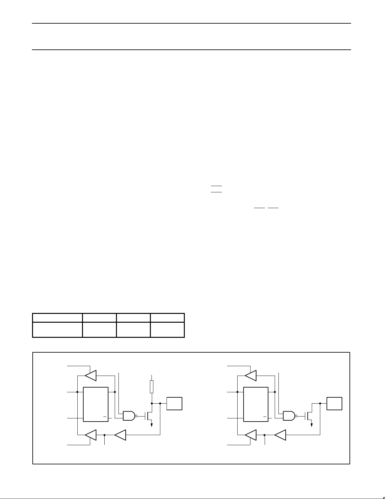
See Figure 1 for port bit configurations.
P1.X
LATCH
D Q
CL Q
READ
LATCH
INT. BUS
WRITE TO
LATCH
READ
PIN
ALTERNATE INPUT
FUNCTION
V
DD
P1.X
PIN
INTERNAL
PULL-UP
ALTERNATE
OUTPUT
FUNCTION
P0.X
LATCH
D Q
CL Q
READ
LATCH
INT. BUS
WRITE TO
LATCH
READ
PIN
ALTERNATE INPUT
FUNCTION
P0.X
PIN
ALTERNATE
OUTPUT
FUNCTION
SU00306
Figure 1. Port Bit Latches and I/O Buffers
Page 6
Philips Semiconductors Product specification
TPM749Microcontroller with TrackPoint microcode from IBM
1996 May 01
6
R
S
V
ANALOG
INPUT
C
S
C
C
To Comparator
+
I
N
I
N+1
Sm
N+1
Sm
N
Rm
N+1
Rm
N
Multiplexer
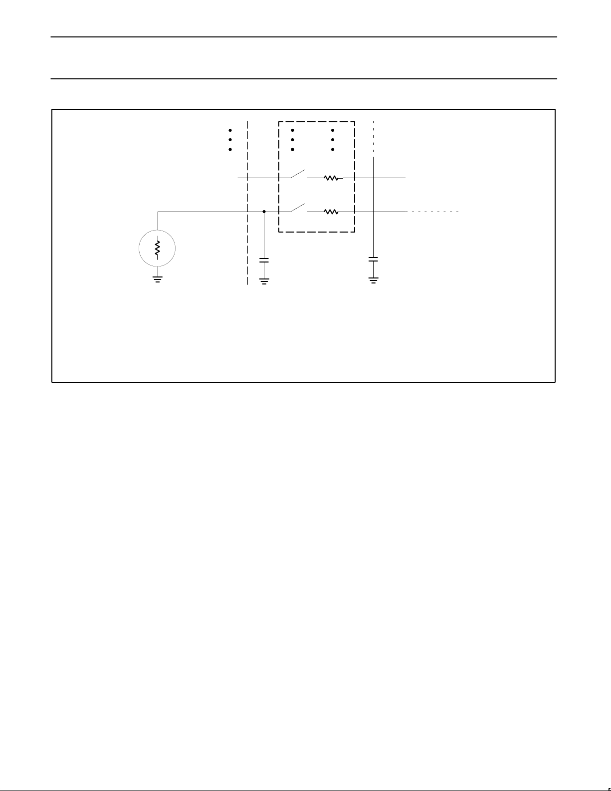
Rm = 0.5 - 3 kΩ
CS + CC = 15pF maximum
RS = Recommended < 9.6 kΩ for 1 LSB @ 12MHz
NOTE:
Because the analog to digital converter has a sampled-data comparator, the input looks capacitive to a source. When a conversion
is initiated, switch Sm closes for 8tcy (8µs @ 12MHz crystal frequency) during which time capacitance Cs + Cc is charged. It should
be noted that the sampling causes the analog input to present a varying load to an analog source.
SU00199
Figure 2. A/D Input: Equivalent Circuit
A/D CONVERTER PARAMETER DEFINITIONS
The following definitions are included to clarify some specifications
given and do not represent a complete set of A/D parameter
definitions.
Absolute Accuracy Error
Absolute accuracy error of a given output is the difference between
the theoretical analog input voltage to produce a given output and
the actual analog input voltage required to produce the same code.
Since the same output code is produced by a band of input voltages,
the “required input voltage” is defined as the midpoint of the band of
input voltage that will produce that code. Absolute accuracy error
not specified with a code is the maximum over all codes.
Nonlinearity
If a straight line is drawn between the end points of the actual
converter characteristics such that zero offset and full scale errors
are removed, then non-linearity is the maximum deviation of the
code transitions of the actual characteristics from that of the straight
line so constructed. This is also referred to as relative accuracy and
also integral non-linearity.
Differential Non-Linearity
Differential non-linearity is the maximum difference between the
actual and ideal code widths of the converter. The code widths are
the differences expressed in LSB between the code transition
points, as the input voltage is varied through the range for the
complete set of codes.
Gain Error
Gain error is the deviation between the ideal and actual analog input
voltage required to cause the final code transition to a full-scale
output code after the offset error has been removed. This may
sometimes be referred to as full scale error.
Offset Error
Offset error is the difference between the actual input voltage that
causes the first code transition and the ideal value to cause the first
code transition. This ideal value is 1/2 LSB above V
ref–
.
Channel to Channel Matching
Channel to channel matching is the maximum difference between
the corresponding code transitions of the actual characteristics
taken from different channels under the same temperature, voltage
and frequency conditions.
Crosstalk
Crosstalk is the measured level of a signal at the output of the
converter resulting from a signal applied to one deselected channel.
Total Error
Maximum deviation of any step point from a line connecting the ideal
first transition point to the ideal last transition point.
Relative Accuracy
Relative accuracy error is the deviation of the ADC’s actual code
transition points from the ideal code transition points on a straight
line which connects the ideal first code transition point and the final
code transition point, after nullifying offset error and gain error. It is
generally expressed in LSBs or in percent of FSR.
Page 7

Philips Semiconductors Product specification
TPM749Microcontroller with TrackPoint microcode from IBM
1996 May 01
7
ABSOLUTE MAXIMUM RATINGS
1, 3, 4
PARAMETER
RATING UNIT
Storage temperature range –65 to +150 °C
Voltage from V
CC
to V
SS
–0.5 to +6.5 V
Voltage from any pin to VSS (except VPP) –0.5 to VCC + 0.5 V
Power dissipation 1.0 W
Voltage from VPP pin to V
SS
–0.5 to + 13.0 V
NOTES ON PAGE 8.
DC ELECTRICAL CHARACTERISTICS
T
amb
= 0°C to +70°C, AVCC = 5V ±5, AVSS = 0V
4
VCC = 5V ± 10%, VSS = 0V
TEST LIMITS
4
SYMBOL PARAMETER CONDITIONS MIN TYP
1
MAX UNIT
I
CC
Supply current (see Figure 5)
Inputs
V
IL
Input low voltage –0.5 0.2VCC–0.1 V
V
IH
Input high voltage, except X1, RST 0.2VCC+0.9 VCC+0.5 V
V
IH1
Input high voltage, X1, RST 0.7V
CC
VCC+0.5 V
P0.2
V
IL1
Input low voltage –0.5 0.3V
CC
V
V
IH2
Input high voltage 0.7V
CC
VCC+0.5 V
Outputs
V
OL
Output low voltage, ports 1, 3, 0.3, and 0.4
(PWM disabled)
IOL = 1.6mA
2
0.45 V
V
OL1
Output low voltage, port 0.2 IOL = 3.2mA
2
0.45 V
V
OH
Output high voltage, ports 1, 3, 0.3, and 0.4
(PWM disabled)
IOH = –60µA, 2.4 V
IOH = –25µA 0.75V
CC
V
IOH = –10µA 0.9V
CC
V
IOH = –400µA 2.4 V
V
OH2
Output high voltage, P0.4 (PWM enabled) IOH = –40µA 0.9V
CC
V
Port 0.0 and 0.1 – Drivers
V
OL2
Output low voltage
(over VCC range)
0.4 V
C
Driver, receiver combined:
Capacitance
10 pF
I
IL
Logical 0 input current,
ports 1, 3, 0.3, and 0.4 (PWM disabled)
11
VIN = 0.45V –50 µA
I
TL
Logical 1 to 0 transition current,
ports 1, 3, 0.3 and 0.4
11
VIN = 2V –650 µA
I
LI
Input leakage current, port 0.0, 0.1 and 0.2 0.45 < VIN < V
CC
±10 µA
R
RST
Reset pull-down resistor 25 175 kΩ
C
IO
Pin capacitance Test freq = 1MHz,
T
amb
= 25°C
10 pF
I
PD
Power-down current
5
VCC = 2 to 5.5V
V
CC
= 2 to 6.0V
50 µA
NOTES ON FOLLOWING PAGE.
IOL = 3mA
Page 8

Philips Semiconductors Product specification
TPM749Microcontroller with TrackPoint microcode from IBM
1996 May 01
8
DC ELECTRICAL CHARACTERISTICS (Continued)
T
amb
= 0°C to +70°C, AVCC = 5V ±5, AVSS = 0V
4
VCC = 5V ± 10%, VSS = 0V
TEST LIMITS
4
SYMBOL PARAMETER CONDITIONS MIN TYP
1
MAX UNIT
Analog Inputs (A/D guaranteed only with quartz window covered.)
AV
CC
Analog supply voltage
10
AVCC = VCC±0.2V 4.5 5.5 V
AI
CC
Analog operating supply current AVCC = 5.12V 3
9
mA
AV
IN
Analog input voltage AVSS–0.2 AVCC+0.2 V
C
IA
Analog input capacitance 15 pF
t
ADS
Sampling time 8t
CY
s
t
ADC
Conversion time 40t
CY
s
Analog Inputs (A/D guaranteed only with quartz window covered.) (Continued)
R Resolution 8 bits
E
RA
Relative accuracy ±1 LSB
OS
e
Zero scale offset ±1 LSB
G
e
Full scale gain error 0.4 %
M
CTC
Channel to channel matching ±1 LSB
C
t
Crosstalk 0–100kHz –60 dB
NOTES:
1. Stresses above those listed under Absolute Maximum Ratings may cause permanent damage to the device. This is a stress rating only and
functional operation of the device at these or any conditions other than those described in the AC and DC Electrical Characteristics section
of this specification is not implied.
2. Under steady state (non-transient) conditions, I
OL
must be externally limited as follows:
Maximum I
OL
per port pin: 10mA
Maximum I
OL
per 8-bit port: 26mA
Maximum total I
OL
for all outputs: 67mA
If I
OL
exceeds the test condition, VOL may exceed the related specification. Pins are not guaranteed to sink current greater than the listed
test conditions.
3. This product includes circuitry specifically designed for the protection of its internal devices from the damaging effects of excessive static
charge. Nonetheless, it is suggested that conventional precautions be taken to avoid applying greater than the rated maxima.
4. Parameters are valid over operating temperature range unless otherwise specified. All voltages are with respect to V
SS
unless otherwise
noted.
5. Power-down I
CC
is measured with all output pins disconnected; port 0 = VCC; X2, X1 n.c.; RST = VSS.
6. I
CC
is measured with all output pins disconnected; X1 driven with t
CLCH
, t
CHCL
= 5ns, VIL = VSS + 0.5V, VIH = VCC – 0.5V; X2 n.c.;
RST = port 0 = V
CC
. ICC will be slightly higher if a crystal oscillator is used.
7. Idle I
CC
is measured with all output pins disconnected; X1 driven with t
CLCH
, t
CHCL
= 5ns, VIL = VSS + 0.5V, VIH = VCC – 0.5V; X2 n.c.;
port 0 = V
CC;
RST = VSS.
8. Load capacitance for ports = 80pF.
9. The resistor ladder network is not disconnected in the power down or idle modes. Thus, to conserve power, the user may remove AV
CC
.
10.If the A/D function is not required, or if the A/D function is only needed periodically, AV
CC
may be removed without affecting the operation of
the digital circuitry. Contents of ADCON and ADAT are not guaranteed to be valid. If AV
CC
is removed, the A/D inputs must be lowered to
less than 0.5V. Digital inputs on P1.0–P1.4 will not function normally.
11.These parameters do not apply to P1.0–P1.4 if the A/D function is enabled.
Page 9
Philips Semiconductors Product specification
TPM749Microcontroller with TrackPoint microcode from IBM
1996 May 01
9
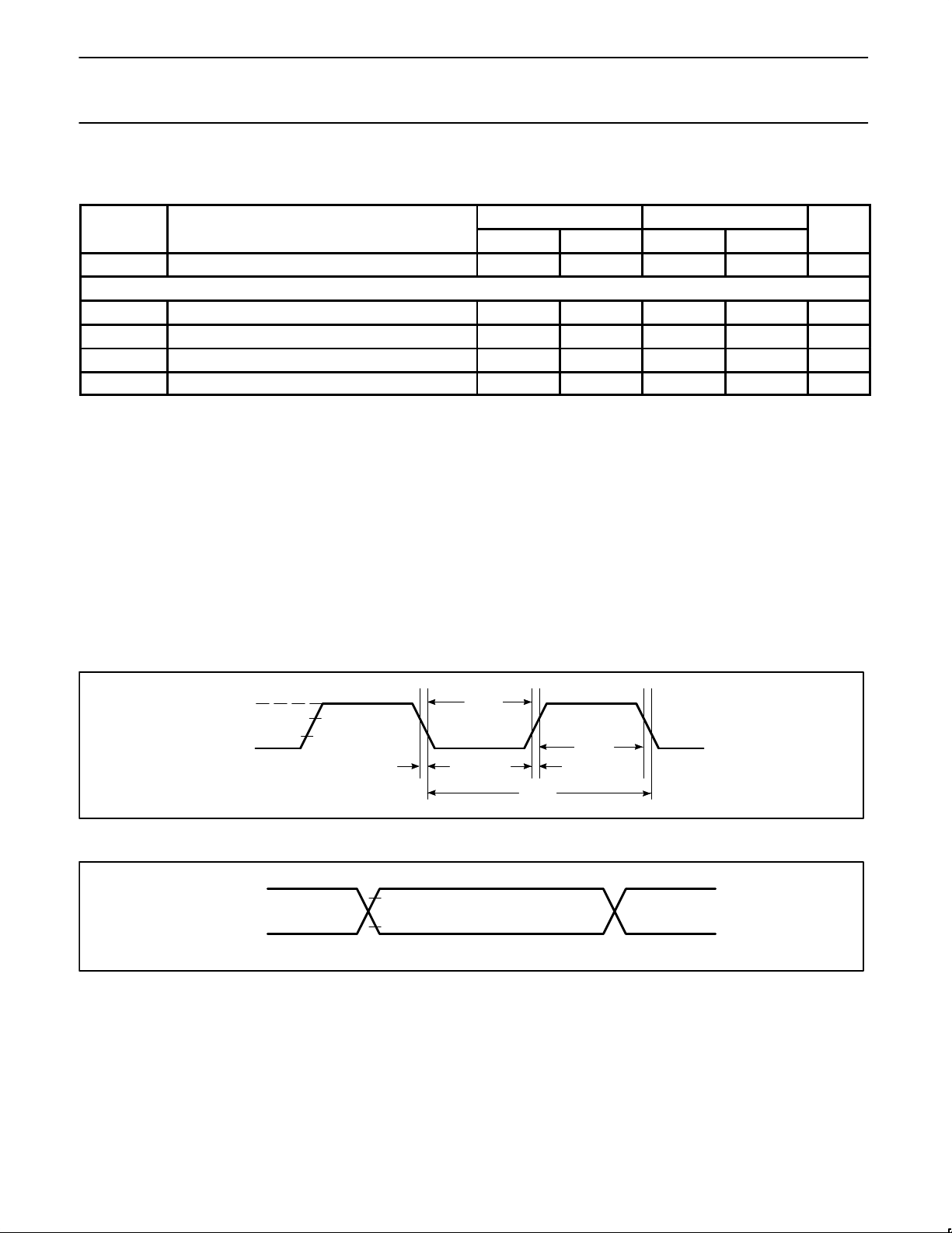
AC ELECTRICAL CHARACTERISTICS
T
amb
= 0°C to +70°C, VCC = 5V ±10%, VSS = 0V
4, 8
12MHz CLOCK VARIABLE CLOCK
SYMBOL PARAMETER MIN MAX MIN MAX UNIT
1/t
CLCL
Oscillator frequency: 3.5 12 MHz
External Clock (Figure 3)
t
CHCX
High time 20 20 ns
t
CLCX
Low time 20 20 ns
t
CLCH
Rise time 20 20 ns
t
CHCL
Fall time 20 20 ns
EXPLANATION OF THE AC SYMBOLS
Each timing symbol has five characters. The first character is always
‘t’ (= time). The other characters, depending on their positions,
indicate the name of a signal or the logical status of that signal. The
designations are:
C – Clock
D – Input data
H – Logic level high
L – Logic level low
Q – Output data
T – Time
V – Valid
X – No longer a valid logic level
Z – Float
t
CHCL
t
CLCL
t
CLCH
t
CHCX
VCC –0.5
0.45V
0.2 V
CC
+ 0.9
0.2 V
CC
– 0.1
t
CLCX
SU00297
0.2 VCC + 0.9
0.2 VCC – 0.1
VCC –0.5
0.45V
SU00307
Figure 3. External Clock Drive
Figure 4. AC Testing Input/Output
Page 10

Philips Semiconductors Product specification
TPM749Microcontroller with TrackPoint microcode from IBM
1996 May 01
10
I
CC
mA
2
4
6
8
10
12
14
16
18
20
22
SU00693
Maximum I
MAX ACTIVE I
TYP ACTIVE I
MAX IDLE I
TYP IDLE I
4MHz 8MHz 12MHz
FREQ
CC
CC
CC
Figure 5. ICC vs. FREQ
values taken at VCC = 5.5V and worst case temperature.
CC
Typical I
Notes 6 and 7 refer to AC Electrical Characteristics.
values taken at VCC = 5.0V and 25°C.
CC
CC
7
6
6
7
Page 11
Philips Semiconductors Product specification
TPM749Microcontroller with TrackPoint microcode from IBM
11
1996 May 01
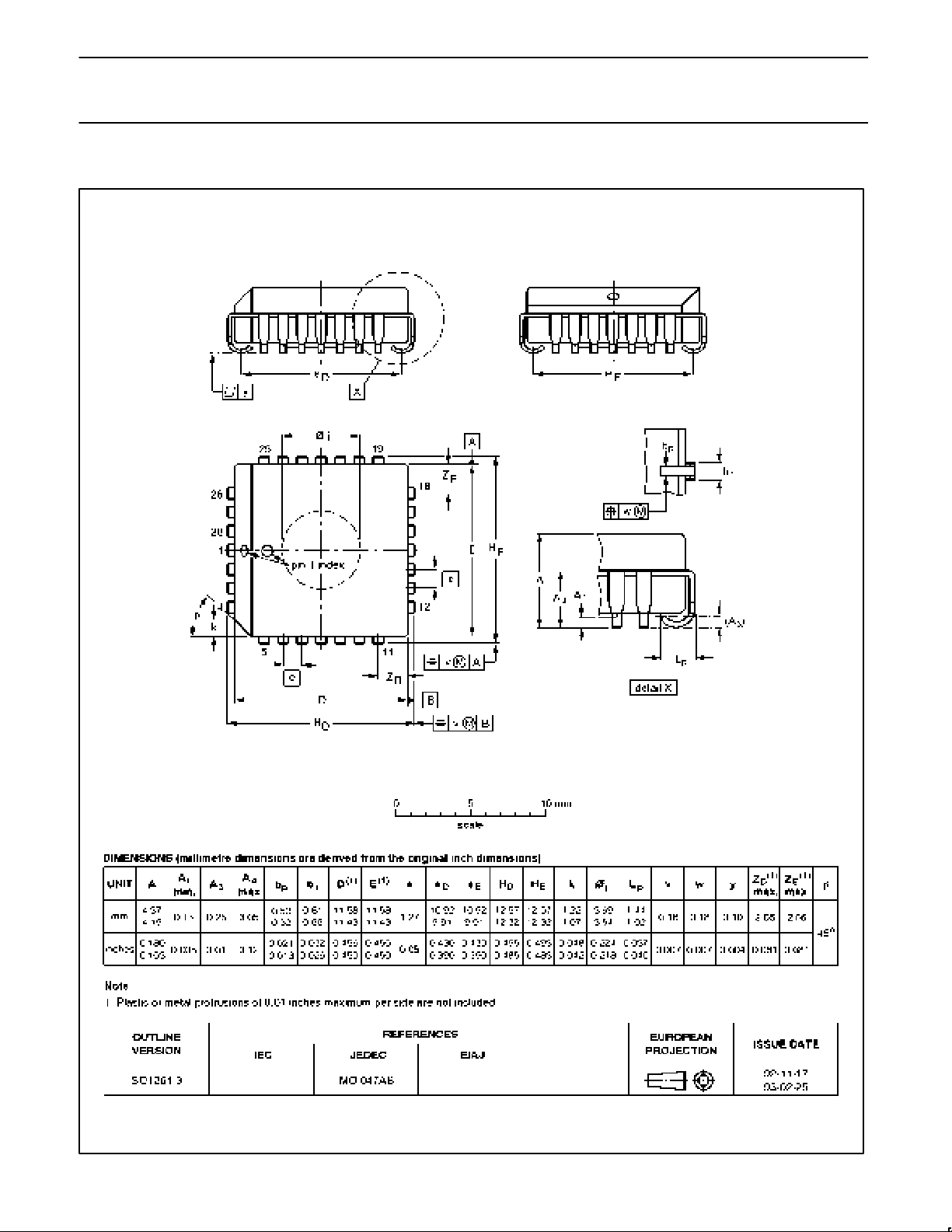
PLCC28: plastic leaded chip carrer; 28 leads; pedestal SOT261-3
Page 12
Philips Semiconductors Product specification
TPM749Microcontroller with TrackPoint microcode from IBM
1996 May 01
12
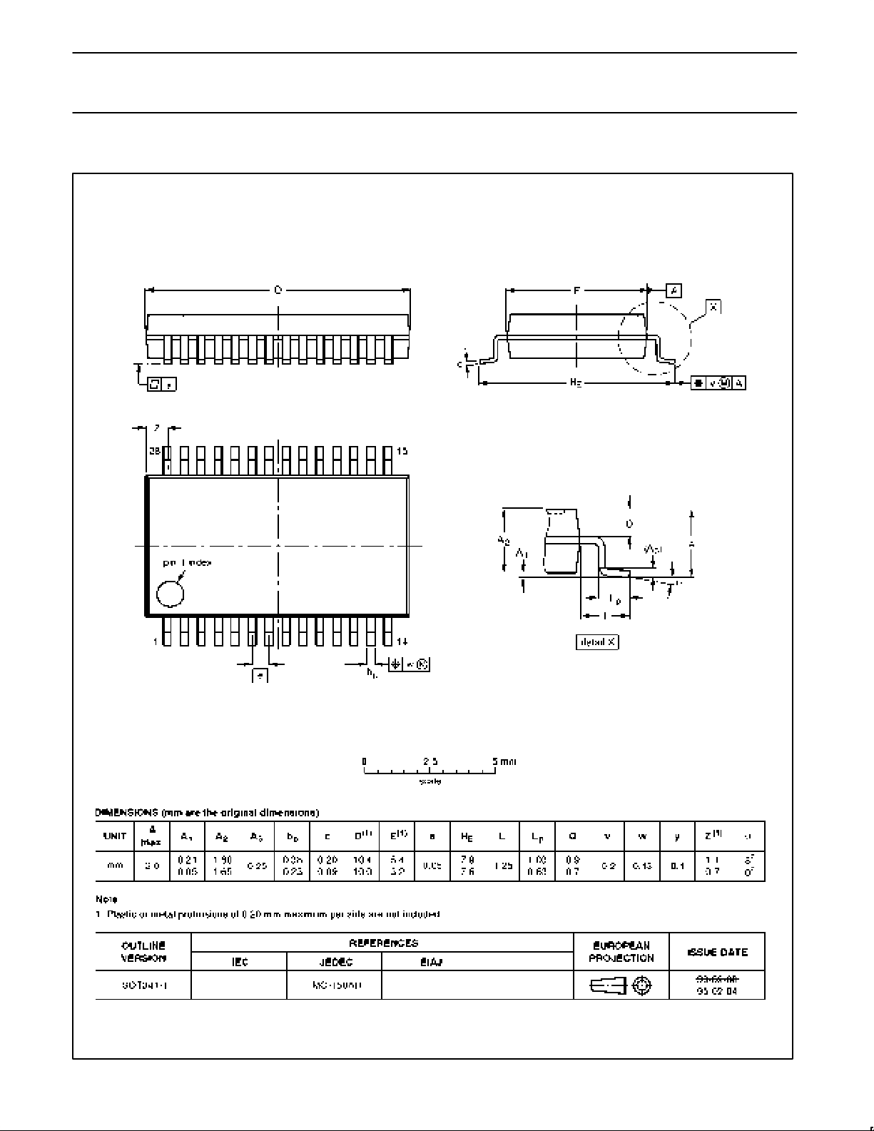
SSOP28: plastic shrink small outline package; 28 leads; body width 5.3mm SOT341-1
Page 13

Philips Semiconductors Product specification
TPM749Microcontroller with TrackPoint microcode from IBM
1996 May 01
13
NOTES
Page 14

Philips Semiconductors Product specification
TPM749Microcontroller with TrackPoint microcode from IBM
458291/4M/FP/pp16 Date of release: 05/96
Document order number: 9397 750 00817
Philips Semiconductors and Philips Electronics North America Corporation reserve the right to make changes, without notice, in the products,
including circuits, standard cells, and/or software, described or contained herein in order to improve design and/or performance. Philips
Semiconductors assumes no responsibility or liability for the use of any of these products, conveys no license or title under any patent, copyright,
or mask work right to these products, and makes no representations or warranties that these products are free from patent, copyright, or mask
work right infringement, unless otherwise specified. Applications that are described herein for any of these products are for illustrative purposes
only. Philips Semiconductors makes no representation or warranty that such applications will be suitable for the specified use without further testing
or modification.
LIFE SUPPORT APPLICATIONS
Philips Semiconductors and Philips Electronics North America Corporation Products are not designed for use in life support appliances, devices,
or systems where malfunction of a Philips Semiconductors and Philips Electronics North America Corporation Product can reasonably be expected
to result in a personal injury. Philips Semiconductors and Philips Electronics North America Corporation customers using or selling Philips
Semiconductors and Philips Electronics North America Corporation Products for use in such applications do so at their own risk and agree to fully
indemnify Philips Semiconductors and Philips Electronics North America Corporation for any damages resulting from such improper use or sale.
This data sheet contains preliminary data, and supplementary data will be published at a later date. Philips
Semiconductors reserves the right to make changes at any time without notice in order to improve design
and supply the best possible product.
Philips Semiconductors
811 East Arques Avenue
P.O. Box 3409
Sunnyvale, California 94088–3409
Telephone 800-234-7381
DEFINITIONS
Data Sheet Identification Product Status Definition
Objective Specification
Preliminary Specification
Product Specification
Formative or in Design
Preproduction Product
Full Production
This data sheet contains the design target or goal specifications for product development. Specifications
may change in any manner without notice.
This data sheet contains Final Specifications. Philips Semiconductors reserves the right to make changes
at any time without notice, in order to improve design and supply the best possible product.
Philips Semiconductors and Philips Electronics North America Corporation
register eligible circuits under the Semiconductor Chip Protection Act.
Copyright Philips Electronics North America Corporation 1996
All rights reserved. Printed in U.S.A.
 Loading...