

Page 1
TPIC44H01
4-CHANNEL SERIAL AND PARALLEL HIGH-SIDE PRE-FET DRIVER
SLIS088 – SEPTEMBER 1998
1
POST OFFICE BOX 655303 • DALLAS, TEXAS 75265
D
Serial or Parallel Control of Gate Outputs
D
Sleep State for Low Quiescent Current
D
Independent On-State Source
Short-to-Ground (Shorted-Load)
Detection/Protection
D
Independent On-State Over-Current
Detection/Protection With Dynamic Fault
Threshold
D
Independent Off-State Open-Load
Detection
D
Supply Over-Voltage Lockout Protection
D
Asynchronous Open-Drain Fault Interrupt
Terminal to Flag Fault Conditions. Output
Can be OR’ed With Multiple Devices
D
Encoded Fault Status Reporting Through
Serial Output Terminal (2-Bits Per Channel)
D
Programmable On-State Fault Deglitch
Timers
D
High Impedance CMOS Compatible Inputs
With Hysteresis
D
Fault Mode Selection: Outputs Latched Off
or Switched at Low Duty Cycle
D
Device Can be Cascaded With Serial
Interface
description
The TPIC44H01 is a four channel high-side pre-FET driver which provides serial or parallel input interface to
control four external NMOS power FETs. It is designed for use in low frequency switching applications for
resistive or inductive loads, including solenoids and incandescent bulbs.
Each channel has over-current, short-to-ground, and open-load detection that is flagged through the FLT
pin
and distinguished through the serial interface. Over-current thresholds are set through the V
(PK_x)
and
V
(COMP1-4)
pins. Short-to-ground and open-load thresholds are set internally to approximately 2.5 V. The
AR_ENBL pin is used to define the operation of the device during a fault condition, allowing the outputs to either
latch off or to enter a low duty cycle, auto-retry mode. An over-voltage lockout circuit on V
(PWR)
protects the
device and the external FETs. A low current sleep state mode is provided to allow the TPIC44H01 to be used
in applications where V
(PWR)
is connected directly to the battery. An internal charge pump allows the use of
N-channel FET s for high-side drive applications, while current-limit gate drive provides slope control for reduced
RFI.
By having the unique ability to develop a dynamic over-current threshold, the TPIC44H01 can be used to drive
incandescent bulbs with long inrush currents without falsely flagging a fault. Likewise, the user can select an
internally set over-current threshold of ~1.25 V by pulling the respective V
(COMP1-4)
pin to VCC.
Copyright 1998, Texas Instruments Incorporated
PRODUCTION DATA information is current as of publication date.
Products conform to specifications per the terms of Texas Instruments
standard warranty. Production processing does not necessarily include
testing of all parameters.
Please be aware that an important notice concerning availability, standard warranty, and use in critical applications of
Texas Instruments semiconductor products and disclaimers thereto appears at the end of this data sheet.
TI is a trademark of Texas Instruments Incorporated.
1
2
3
4
5
6
7
8
9
10
11
12
13
14
15
16
32
31
30
29
28
27
26
25
24
23
22
21
20
19
18
17
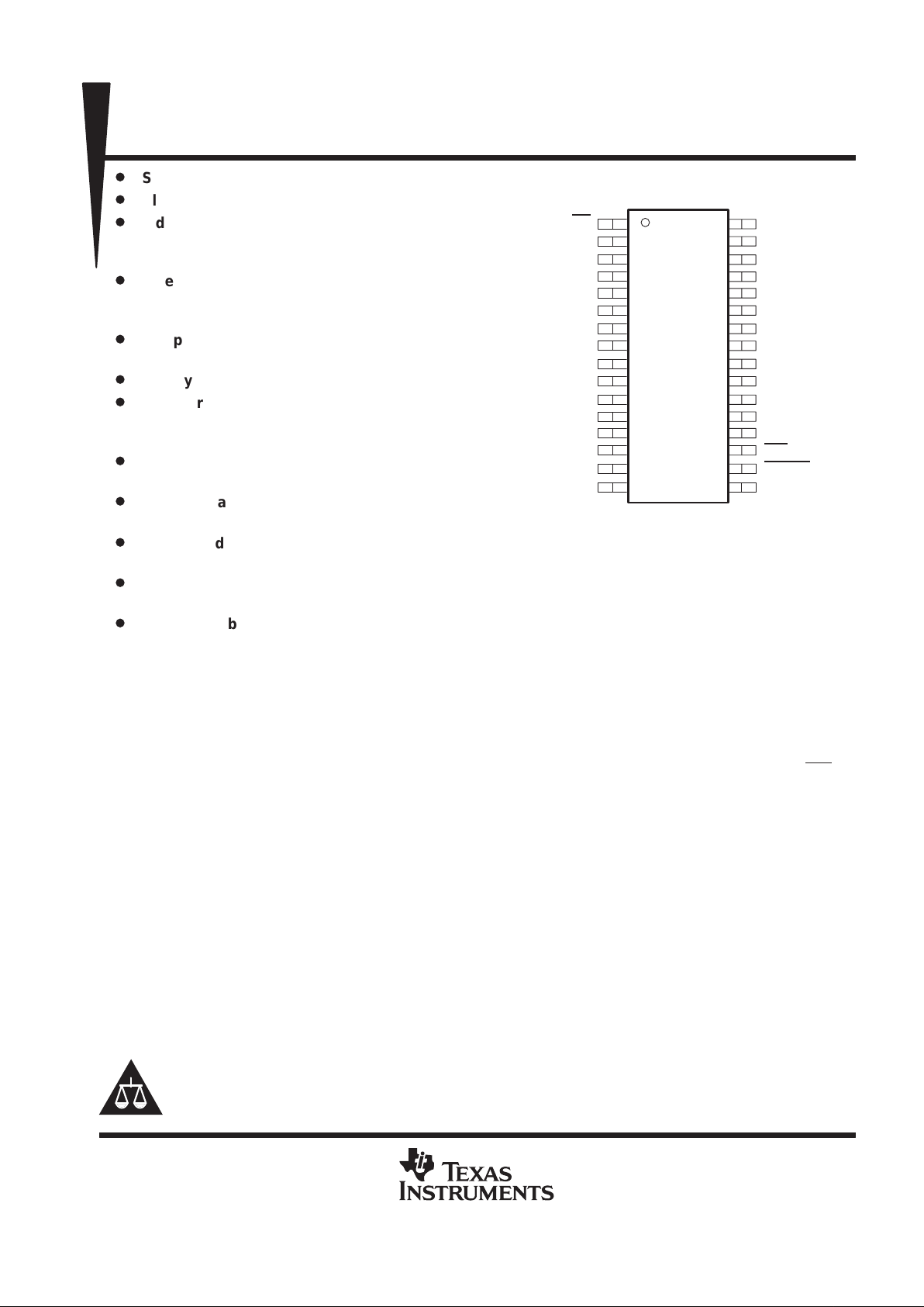
CS
SD0
SDI
SCLK
AR_ENBL
GND
IN1
IN2
IN3
IN4
V
CC
V
(PK_A)
V
(PK_B)
V
(COMP1)
V
(COMP2)
V
(COMP3)
PGND
V
(PWR)
CP1
CP2
V
(CP)
GATE1
SRC1
GATE2
SRC2
GATE3
SRC3
GATE4
SRC4
FL T
RESET
V
(COMP4)
DA PACKAGE
(TOP VIEW)
Page 2

TPIC44H01
4-CHANNEL SERIAL AND PARALLEL HIGH-SIDE PRE-FET DRIVER
SLIS088 – SEPTEMBER 1998
2
POST OFFICE BOX 655303 • DALLAS, TEXAS 75265
description (continued)
The 8-bit serial peripheral interface (SPI) allows the user to command any of the four outputs on or off, to
program one of eight possible open-load, over-current, and short-load fault deglitch timer settings, and to
engage the sleep state. Data is clocked into the SDI pin on the rising edge of SCLK and clocked out of the SDO
pin on the SCLK falling edge. The serial input bits are logic OR’ed with the IN1-IN4 parallel inputs pins. The serial
interface is also used to read normal-load, open-load, over-current, and short-to-ground conditions for each
channel. Over-voltage lockout can be detected when the FL T
pin is low and no bits are set in the SDO register.
Multiple TPIC44H01 devices may be cascaded together using the serial interface to further reduce I/O lines from
the host controller.
Page 3
TPIC44H01
4-CHANNEL SERIAL AND PARALLEL HIGH-SIDE PRE-FET DRIVER
SLIS088 – SEPTEMBER 1998
3
POST OFFICE BOX 655303 • DALLAS, TEXAS 75265
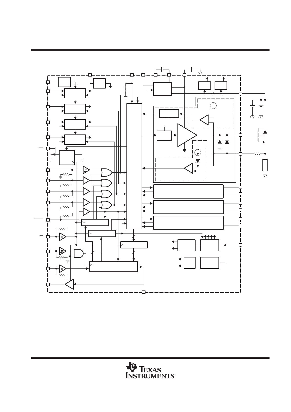
schematic/block diagram
V
V
peak
Buffer
V
(PK_A)
OVDS V
thres
Generation
OVDS V
thres
Generation
V
(COMP1)
V
bg
V
(COMP2)
V
bg
OVDS V
thres1
OVDS V
thres2
V
peakA
V
peakA
OVDS V
thres
Generation
V
(COMP3)
V
bg
OVDS V
thres3
V
peakB
OVDS V
thres
Generation
V
(COMP4)
V
bg
OVDS V
thres4
V
peakB
QD
CLK
PS
FLT
IN1
IN2
IN3
IN4
V
CC
RESET
V
peak
Buffer
V
peakB
V
(PK_B)
Parallel Reg
Control Reg
V
CC
CS
Sleep
t
DG
Gate Drive and
Fault Protection Logic
AR_ENBL
OVLO
Charge
Pump
0.01 µF
CP
0.1 µF
CS
PGND
CP1
CP2
V
(CP)
OVLO
OSC
5-V
V
reg
OVLO 5-V Int
+
–
OVDS
V
thres
+
–
OVDS t
DG
Comp
Over-V
DS
Detect
HS Gate
Drive
Gate
Control
+
–
7-V Int
+
–
Comp
I
5-V Int
2 V
bg
On-State ShortLoad Detect
Off-State OpenLoad Detect
Channel 1
Output
Channel 2 Output
Channel 3 Output
Channel 4 Output
GATE2
SRC2
GATE3
SRC3
GATE4
SRC4
Global
Ibias
Band Gap
I
bias
Sleep
8
Fault Logic
Serial Shift Register
4 4
SCLK
SDI
SDO
Tri-State Buffer
2 V
bg
V
bg
UVLO/
POR
OSC
Charge Pump
Digital Deglitch
V
CC
0.1 µF1 µF
+
LOAD
100 Ω
SRC1
GATE1
V
(PWR)
8
t
AR
GND
Page 4
TPIC44H01
4-CHANNEL SERIAL AND PARALLEL HIGH-SIDE PRE-FET DRIVER
SLIS088 – SEPTEMBER 1998
4
POST OFFICE BOX 655303 • DALLAS, TEXAS 75265
Terminal Functions
PIN PIN
NO. NAME
I/O
DESCRIPTION
1 CS I Chip Select. CS is an active low, logic level input with internal pullup. A logic level low on CS enables the
serial interface and refreshes the fault interrupt (FLT
). A high on CS enables the serial register to serve as
the fault data register.
2 SDO O Serial Data Output. SDO is a logic level, tri-state output that transfers fault data to the host controller. Serial
input data passes to the next stage for cascade operation. SDO is forced into a high impendance state when
CS
terminal is in a high state. When CS is in a low state, data is clocked out on each falling edge of SCLK.
3 SDI I Serial Data Input. SDI is a logic level input with hysteresis and internal pulldown. Gate drive output control
data is clocked into the serial register using SDI. A high SDI bit programs a particular gate output on, and a
low turns it off, as long as the parallel input is off (OR function).
4 SCLK I Serial Clock. SCLK is a logic level input with hysteresis and internal pulldown. SCLK clocks data at the SDI
terminal into the input serial shift register on each rising edge, and shifts out fault data (and serial input data
for cascaded operation) to the SDO pin on each falling edge.
5 AR_ENBL I Auto-Retry Enable. AR_ENBL is a logic level input with hysteresis and internal pulldown. When
AR_ENBL=0, an over-current/short-to-ground fault latches the channel off. When AR_ENBL = 1, an
over-current/short-to-ground fault engages a low duty cycle operation.
6 GND I Analog ground and substrate connection
7–10 IN1-4 I Parallel Inputs. IN1-4 are logic level inputs with hysteresis and internal pulldown. IN1–4 provide real-time
control of gate pre-drive circuitry. A high on IN1-4 will turn on corresponding gate drive outputs (GATE1-4).
Gate output status is a logic OR function of the parallel inputs and the serial input bits.
11 V
CC
I 5-V logic supply voltage
12 V
(PK_A)
I Dynamic over-current fault threshold peak voltage that is shared by channels 1 and 2
13 V
(PK_B)
I Dynamic over-current fault threshold peak voltage that is shared by channels 3 and 4
14–17 V
(COMP1-4)
I Fault Reference Voltage. V
(COMP1–4)
are used to provide an external fault reference voltage for the
over-current fault detection circuitry. It is also used to generate a dynamic threshold when used in conjunction
with V
(PK_x)
. To guarantee V
(COMP)
stability, a minimum of 100 pF capacitance should be placed from
V
(COMP)
to ground.
18 RESET I Reset. RESET is an active low, logic level input with hysteresis and internal pullup. A low on RESET clears
all registers and fault bits. All gate outputs are turned off and a latched FLT
interrupt is cleared.
19 FLT O Fault Interrupt. FLT is an active low , logic level, open-drain output providing real-time latched fault interrupts
for fault detection. A latched FLT
is cleared only by a low on CS. The FLT terminal can be OR’ed with other
devices for fault interrupt handling. An external pullup is required.
20, 22,
24, 26
SRC1-4 I FET Source Inputs. These inputs are used for both open-load and over-current fault detection at the source
of the external FETs.
21, 23,
25, 27
GATE1-4 O Gate Drive Outputs. Output voltage is derived from V
(CP)
supply voltage. Internal clamps prevent the voltage
on these nodes, with respect to SRC1-4, from exceeding the VGS rating of most FETs.
28 V
(CP)
O Charge pump voltage storage capacitor and supply pin to high-side gate drives
29 CP2 O Charge pump capacitor terminal
30 CP1 O Charge pump capacitor terminal
31 V
(PWR)
I Power supply voltage input
32 PGND I Power ground for charge pump
Page 5
TPIC44H01
4-CHANNEL SERIAL AND PARALLEL HIGH-SIDE PRE-FET DRIVER
SLIS088 – SEPTEMBER 1998
5
POST OFFICE BOX 655303 • DALLAS, TEXAS 75265
absolute maximum ratings over operating free-air temperature (unless otherwise noted)
†
Logic supply voltage range, V
CC
(see Note 1) –0.3 V to 7 V. . . . . . . . . . . . . . . . . . . . . . . . . . . . . . . . . . . . . . . . .
Power supply voltage range, V
(PWR)
(see Note 1) –0.3 V to 40 V. . . . . . . . . . . . . . . . . . . . . . . . . . . . . . . . . . . .
Input voltage range, V
I
(see Note 1) –0.3 V to 7 V. . . . . . . . . . . . . . . . . . . . . . . . . . . . . . . . . . . . . . . . . . . . . . . . . .
Output voltage range, V
O
(SDO and FLT, see Note 1) –0.3 V to 7 V. . . . . . . . . . . . . . . . . . . . . . . . . . . . . . . . . .
Source input voltage, V
I(SRCx)
(see Note 1) –3 V to 40 V. . . . . . . . . . . . . . . . . . . . . . . . . . . . . . . . . . . . . . . . . . . .
Output voltage, V
O(GA TEx)
(see Note 1) –0.3 V to 45 V. . . . . . . . . . . . . . . . . . . . . . . . . . . . . . . . . . . . . . . . . . . . .
Logic input current, I
I
±25 µA. . . . . . . . . . . . . . . . . . . . . . . . . . . . . . . . . . . . . . . . . . . . . . . . . . . . . . . . . . . . . . . . . . . .
Operating case temperature range, T
C
–40°C to 125°C. . . . . . . . . . . . . . . . . . . . . . . . . . . . . . . . . . . . . . . . . . . . .
Operating virtual junction temperature range, T
J
–40°C to 150°C. . . . . . . . . . . . . . . . . . . . . . . . . . . . . . . . . . . . .
Storage temperature range, T
stg
–65°C to 150°C. . . . . . . . . . . . . . . . . . . . . . . . . . . . . . . . . . . . . . . . . . . . . . . . . . .
†
Stresses beyond those listed under “absolute maximum ratings” may cause permanent damage to the device. These are stress ratings only, and
functional operation of the device at these or any other conditions beyond those indicated under “recommended operating conditions” is not
implied. Exposure to absolute-maximum-rated conditions for extended periods may affect device reliability.
NOTE 1: All voltage values are with respect to GND.
recommended operating conditions
MIN TYP MAX UNIT
Logic supply voltage, V
CC
4.5 5 5.5 V
Power supply voltage, V
(PWR)
8 24 V
High level logic input voltage, VIH (all logic inputs except RESET) 0.7×V
CC
V
CC
V
Low level logic input voltage, VIL (all logic inputs except RESET) 0 0.3×V
CC
V
Setup time, SDI high before SCLK rising edge, tsu (see Figure 5) 10 ns
Hold time, SDI high after SCLK rising edge, th (see Figure 5) 10 ns
Operating case temperature, T
C
–40 125 °C
thermal resistance
PARAMETER TEST CONDITIONS MIN TYP MAX UNIT
R
θJA
Junction-to-ambient thermal resistance Using JEDEC, low K, board configuration 86.04 °C/W
R
θJC
Junction-to-case thermal resistance 7.32 °C/W
Page 6
TPIC44H01
4-CHANNEL SERIAL AND PARALLEL HIGH-SIDE PRE-FET DRIVER
SLIS088 – SEPTEMBER 1998
6
POST OFFICE BOX 655303 • DALLAS, TEXAS 75265
electrical characteristics over recommended operating case temperature and supply voltage
range (unless otherwise noted)
†
PARAMETER TEST CONDITIONS MIN TYP MAX UNIT
I
(PWR)
V
(PWR)
supply current All outputs off, V
(PWR)
= 12 V 2 4 6 mA
I
CCH
5-V supply current All outputs off, VCC = 5.5 V 3 4 5 mA
p
p
p
I
-
p
Slee state current
Slee state (all out uts off)
,
15 40
µ
A
I
(PWR-slee )
(I
PWR
)
V
CC
= 5.5 V,
V
(PWR)
= 12 V,
T
C
=
25°C
15
40
µA
p
p
p
I
p
Slee state current
Slee state (all out uts off)
,
30 40
µ
A
I
CCL(slee )
(I
CCL
)
V
CC
= 5.5 V,
V
(PWR)
= 12 V,
T
C
=
25°C
30
40
µA
V
IT(POR)
Power-on reset
threshold, V
CC
V
(PWR)
= 5.5 V, VCC increasing 3.4 3.9 4.4 V
V
hys(POR)
Power-on reset
threshold hysteresis,
V
CC
V
(PWR)
= 5.5 V, VCC decreasing 100 300 500 mV
V
> 24 V, CP = 0.01 µF, CS = 0.1 µF,
(PWR)
, µ , µ ,
I
(CP)
= –2 mA, See Figure 8
40
44
V
V
(PWR)
= 24 V, CP = 0.01 µF, CS = 0.1 µF,
38 40 42 V
p
p
I
(CP)
= –2 mA, See Figure
8
384042
V
V
(CP)
Charge um voltage
V
= 8 V, CP = 0.01 µF, CS = 0.1 µF,
(PWR)
, µ , µ ,
I
(CP)
= –2 mA, See Figure 8
11.5
13.5
V
V
(PWR)
= 5.5 V, CP = 0.01 µF,
CS = 0.1 µF, I
(CP)
= –2 mA, See Figure 8
6.8 7.5 V
V
(OVLO)
Over-supply voltage
lockout
Gate disabled, See Figure 10 27.5 30 32.5 V
V
hys(OV)
Over-supply voltage
reset hysteresis
See Figure 10 0.5 1 2 V
8 V < V
< 24 V, I
= –100 µA,
(PWR)
,
O
µ ,
All channels on, See Note 2
V
(PWR)
+
4
V
(PWR)
+
18
V
VGGate drive voltage
5.5 V < V
< 8 V, I
= –100 µA,
(PWR)
,
O
µ ,
All channels on, See Note 2
V
(PWR)
+1.
5
V
(PWR)
+3.
5
V
V
G(sleep)
External gate sleep
state voltage
IO = 100 µA, RESET = CS = 0 V 0 100 300 mV
V
GS(clamp)
Gate-to-source clamp
voltage
SRCx = 0 V, Output on 15 17 19.5 V
V
SG(clamp)
Source-to-gate clamp
voltage
Output off, II = 100 µA 6.5 8 9.5 V
Gate drive source
VG = 0 V, V
(PWR)
= 12 V –2.3 –3 –3.7
I
G(SRCx)
current
VG = 10 V, V
(PWR)
= 12 V
–1.4 –2 –2.6
mA
Gate drive sink
VG = 2 V, V
(PWR)
= 12 V 1 1.5 2
I
G(SNKx)
current
VG= V
(PWR)
= 12 V
2 2.6 3.2
mA
V
(open)
SRCx pin off-state
open-load detection
threshold
All outputs off, See Figure 1 1 1.9 2.4 2.6 V
V
hys(open)
Off-state open-load
hysteresis
All outputs off –50 –150 –300 mV
†
Device will function with degraded performance for a power supply voltage between 5.5 V and 8 V .
NOTE 2: For characterization purposes only, not implemented in production testing.
Page 7
TPIC44H01
4-CHANNEL SERIAL AND PARALLEL HIGH-SIDE PRE-FET DRIVER
SLIS088 – SEPTEMBER 1998
7
POST OFFICE BOX 655303 • DALLAS, TEXAS 75265
electrical characteristics over recommended operating case temperature and supply voltage
range (unless otherwise noted)
†
(continued)
PARAMETER TEST CONDITIONS MIN TYP MAX UNIT
I
(open)
Off-state open-load
detection current
All outputs off –20 –50 –70 µA
V
(COMPx)
> VCC – 250 mV 1 1.25 1.5 V
V
(OVDS)
Drain-to-source
-
0.1 V < V
< 2.5 V, 0.95 × V
–15 1.05 × V
+15
()
over voltage
(COMPx)
,
See Figures 12 and 13
(COMPx)
mV
(COMPx)
mV
V
V
(STG)
On-state
short-to-ground
detection voltage
See Figure 17 1.9 2.35 2.6 V
V
hys(STG)
On-state
short-to-ground
hysteresis
–50 –150 –300 mV
I
(pullup)
Logic input pullup
current
(CS
, RESET)
VCC = 5 V, VIN = 0 V –5 –20 –50 µA
I
(pulldown)
Logic input pulldown
current (IN1–4, SCLK,
SDI, AR_ENBL)
VCC = 5 V, VIN = 5 V 5 20 50 µA
V
hys
Logic input voltage
hysteresis (IN1–4,
SCLK, SDI, AR_ENBL,
CS
)
VCC = 5 V 0.5 0.8 1.2 V
V
OH
High level serial output
voltage
IO = –1 mA 0.8×V
CC
4.96 V
V
OL
Low level serial output
voltage
IO = 1 mA 0 100 400 mV
I
OZ
Serial data output
tri-state current
V
(SDO)
= 5.5 V to 0 V,
VCC = 5.5 V
–35 1 35 µA
V
OL(FLT)
FLT low level output
voltage
IO = 220 µA 0 30 350 mV
I
lkg(FLT)
FLT leakage current R
(pullup)
= 25 K, VCC = 5.5 V 0 1 20 µA
V
IH(RESET)
RESET high level logic
input voltage
1.9 2.2 V
CC
V
V
IL(RESET)
RESET low level logic
input voltage
0 1.2 1.4 V
V
hys(RESET)
Logic input voltage
hysteresis (RESET
)
VCC = 5 V 0.6 1 1.4 V
†
Device will function with degraded performance for a power supply voltage between 5.5 V and 8 V .
Page 8
TPIC44H01
4-CHANNEL SERIAL AND PARALLEL HIGH-SIDE PRE-FET DRIVER
SLIS088 – SEPTEMBER 1998
8
POST OFFICE BOX 655303 • DALLAS, TEXAS 75265
switching characteristics, VCC = 5 V, V
(PWR)
= 12 V, TC = 25°C
PARAMETER TEST CONDITIONS MIN TYP MAX UNIT
t
(STG)
Short-to-ground deglitch time 16 µs
t
(OC)
Over-current deglitch time
SDI bits DG1–3 = 0 (default after POR),
120 µs
t
(OL)
Open-load deglitch time
(),
See Figures 11, 12, and 17 and Table 4
120 µs
t
(retry)
Auto-retry time 15 ms
t
PLH
Propagation turn-on delay, CS or IN1–4 to
GATE1–4
p
5 µs
t
PHL
Propagation turn-off delay, CS or IN1–4 to
GATE1–4
C
G
=
400 pF
,
See Figures 1 and 2
5 µs
f
(SCLK)
Serial clock frequency t
(WH)
= t
(WL)
= 0.5/f
(SCLK)
, See Figure 5 1 5 MHz
t
su(lead)
Setup from the falling edge of CS to the
rising edge of SCLK
100 ns
t
su(lag)
Setup from the falling edge of SCLK to
rising edge of CS
See Figure 5
100 ns
t
pd(SDOEN)
Propagation delay from falling edge of CS
to SDO valid
50 ns
t
pd(valid)
Propagation delay from falling edge of
SCLK to SDO valid
RL = 10 kΩ, CL = 200 pF, See Figure 5
50 ns
t
pd(SDODIS)
Propagation delay from rising edge of CS
to SDO Hi-Z state
150 ns
t
f(FLT)
Fall time of FLT output RL = 10 kΩ, CL = 200 pF, See Figure 3 12 ns
t
(active)
POR-to-active status delay, sleep-to-active
status delay
See Figure 4 512 µs
Page 9
TPIC44H01
4-CHANNEL SERIAL AND PARALLEL HIGH-SIDE PRE-FET DRIVER
SLIS088 – SEPTEMBER 1998
9
POST OFFICE BOX 655303 • DALLAS, TEXAS 75265
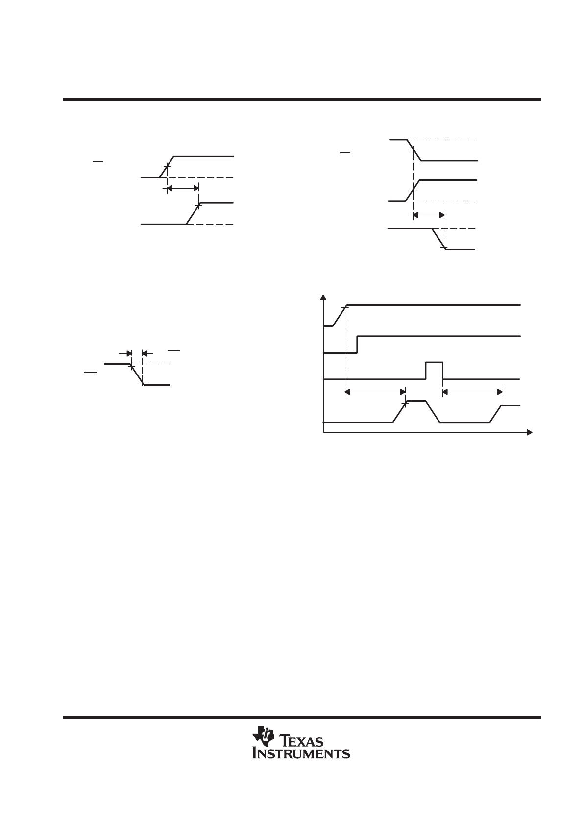
PARAMETER MEASUREMENT INFORMATION
Figure 1. Gate Control Turn-On
t
PLH
V
CC
V
(CP)
0 V
0 V
50%
V
(PWR)
CS
or IN1–4
GATE1–4
90%
Figure 2. Gate Control Turn-Off
50%
50%
V
CC
0 V
t
PHL
10%
V
(CP)
0 V
CS or IN1–4
GATE1–4
V
CC
0 V
Figure 3. Fault Interrupt Fall Time
V
CC
90%
10%
tf
(FLT)
0 V
FLT
Figure 4. Power-Up Waveforms
t
(active)
t
(active)
POR Threshold
V
CC
Input
Internal
Sleep Bit
GATEx
Page 10

TPIC44H01
4-CHANNEL SERIAL AND PARALLEL HIGH-SIDE PRE-FET DRIVER
SLIS088 – SEPTEMBER 1998
10
POST OFFICE BOX 655303 • DALLAS, TEXAS 75265
PARAMETER MEASUREMENT INFORMATION
Figure 5. Serial Interface Timing Diagram
90%
10%
90%
10%
90%
10%
t
su(lead)
t
(WH)
t
(WL)
t
(SCLK)
t
su(lag)
t
su
50%
t
pd(valid)
t
pd(SDOEN)
t
h
FLT
CS
SCLK
SDO
Hi-Z Hi-Z
SDI
Fault Data
Register Latch
(Internal)
Fault Data
Register Refresh
(Internal)
SDO
R
L
C
L
12 7 8
t
pd(SDODIS)
SDO Output Test Schematic
Page 11

TPIC44H01
4-CHANNEL SERIAL AND PARALLEL HIGH-SIDE PRE-FET DRIVER
SLIS088 – SEPTEMBER 1998
11
POST OFFICE BOX 655303 • DALLAS, TEXAS 75265
PRINCIPLES OF OPERATION
serial data operation
The TPIC44H01 offers a serial interface to a host microcontroller to receive control data and to return fault data
to the host controller. For the serial interface operation, it is assumed that all parallel inputs, IN1–4, are low. The
serial interface consists of:
SCLK Serial clock
CS
Chip select (active low)
SDI Serial data input
SDO Serial data output
After a CS
transition from high to low, serial data at the SDI pin is shifted, MSB first, into the serial input shift
register on the low-to-high transition of SCLK. Eight SCLK cycles are required (see T able 1) to shift the first data
bit from LSB to MSB of the shift register. Eight SCLK cycles must occur before a transition from low to high on
CS
to insure proper control of the outputs. Less than eight clock cycles will result in fault data being latched into
the output control buffer . Sixteen bits of data can be shifted into the device, but the first eight bits shifted out are
always the fault data and the last eight bits shifted in are always the output control data. A low-to-high transition
on CS
will latch bits 1–4 of the serial shift register into the output control buffer , bits 5–7 into the deglitch timer
control register, and bit 8 into the sleep state latch. A logic 0 in SDI bit1–4 will turn the corresponding gate drive
output off (providing the parallel input for that channel is at a logic low state); likewise, a logic 1 will turn the output
on. Functionality of bits 5–7 is detailed in T able 4. A logic 1 in SDI bit 8 will enable sleep state and a logic 0 will
maintain normal operation.
Table 1. Serial Data Input Shift Register Bit Assignment
LSB
(Last In)
MSB
(First In)
SDI
B1 B2 B3 B4 B5 B6 B7 B8
IN1 IN2 IN3 IN4 DG1 DG2 DG3 SLEEP
Shift Direction
SDI, Normal Protocol (8–SCLKs)
Table 2. Serial Data Output Shift Register Bit Assignment
MSB
(First Out)
LSB
(Last Out)
SDO
B8 B7 B6 B5 B4 B3 B2 B1
F4B F4A F3B F3A F2B F2A F1B F1A
Shift Direction
SDO, Fault Bit Protocol (8–SCLKs)
Table 3. Fault Bit Encoding
FAULT CONDITION FxB FxA FLT
Normal – no faults X X 1
Over-voltage 0 0 0
Open-load 0 1 0
Over-current 1 0 0
Short-to-ground 1 1 0
Page 12

TPIC44H01
4-CHANNEL SERIAL AND PARALLEL HIGH-SIDE PRE-FET DRIVER
SLIS088 – SEPTEMBER 1998
12
POST OFFICE BOX 655303 • DALLAS, TEXAS 75265
PRINCIPLES OF OPERATION
Table 4. Deglitch Time Encoding
DG1
SDI
BIT5
DG2
SDI
BIT6
DG3
SDI
BIT7
SHORT-TO-GND
DEGLITCH TIME,
t
(STG)
(µs)
SHORT-TO-GND
DUTY CYCLE
WITH:
AR_ENBL=1
OVER-CURRENT
DEGLITCH TIME,
t
(OC)
(µs)
OVER-CURRENT
DUTY CYCLE
WITH:
AR_ENBL=1
AUTO-RETRY
TIME,
t
(retry)
(ms)
OPEN-LOAD
DEGLITCH
TIME, t
(OL
)
(µs)
0 0 0 16
†
0.1%
†
120
†
0.75%
†
16
†
120
†
0 0 1 4 0.1% 30 0.75% 4 30
0 1 0 8 0.1% 60 0.75% 8 60
0 1 1 32 0.1% 240 0.75% 32 240
1 0 0 120 0.1% 120 0.75% 16 120
1 0 1 30 0.1% 30 0.75% 4 30
1 1 0 60 0.1% 60 0.75% 8 60
1 1 1 240 0.1% 240 0.75% 32 240
†
Indicated default conditions after power up.
SDO MSB fault data is setup on the SDO pin by the high-to-low transition of CS prior to the first low-to-high
transition of SCLK. Thus, there must be a lead time, t
su(lead)
(see Figure 5), in the host controller from CS
high-to-low transition to the first rising edge of SCLK to allow the SDO tri-state output to enable and to setup
the fault data MSB on the SDO pin. The remaining 7 bits of fault data are shifted out by the falling edge of the
next 7 SCLK cycles. T o prevent data from prematurely shifting out of SDO on a low transition of CS
while SCLK
is high, the device requires a low-to-high transition on SCLK after a low transition on CS
before the second fault
bit is shifted out. One SCLK cycle is required to clear the serial data register and latch in fault data. If a low
transition on CS
occurs without a low-to-high transition on SCLK, then fault data remains in the SDO register
and the device will not latch data into the control register.
The serial register serves as the fault register while CS
is high. Thus, a fault occurring any time after the end
of the previous serial interface protocol (low-to-high transition of CS
) will be latched as a fault in the serial register
and will be reported via SDO during the next serial protocol. The FLT
interrupt will refresh on the high-to-low
transition of CS
. The CS input must be driven to a high state after the last bit of serial data has been clocked
into the device. The rising edge of CS
will inhibit the SDI input port, put the SDO output port into a high
impedance state, latch the 4 bits of SDI data into the output buffer , and clear/re-enable the serial fault registers
(see Figure 6).
FLT4B FLT4A FLT3B FLT3A FLT2B FLT2A FLT1B FLT1A
Hi-Z Hi-Z
Bit 8 Bit 7 Bit 6 Bit 5 Bit 4 Bit 3 Bit 2 Bit 1
SCLK
CS
SDO
1234567 8
Figure 6. SDO Timing Diagram
The TPIC44H01 serial data interface allows multiple devices to be cascaded together to reduce I/O from the
host controller by using a single CS
line. In this configuration, 8 bits of data for every cascaded TPIC44H01 must
be sent during the time that CS
is low for proper operation (see Figure 7 for an example of two cascaded
TPIC44H01s). If less than 8 bits of data per cascaded device is sent during the time CS
is low, the wrong output
may be enabled or disabled, and some fault data will be latched to the output(s) once CS
returns high.
Page 13

TPIC44H01
4-CHANNEL SERIAL AND PARALLEL HIGH-SIDE PRE-FET DRIVER
SLIS088 – SEPTEMBER 1998
13
POST OFFICE BOX 655303 • DALLAS, TEXAS 75265
PRINCIPLES OF OPERATION
CS
SCLK
SDI
SDO
1st
TPIC44H01
CS
SCLK
MOSI
MISO
µC
CS
SCLK
SDI
SDO
2nd
TPIC44H01
MISO = Master In Slave Out
MOSI = Master Out Slave In
B1
1st
IN1
B2
1st
IN2
B3
1st
IN3
B4
1st
IN4
B5
1st
DG1
B6
1st
DG2
B7
1st
DG3
B8
1st
SLEEP
B1
2nd
IN1
B2
2nd
IN2
B3
2nd
IN3
B4
2nd
IN4
B5
2nd
DG1
B6
2nd
DG2
B7
2nd
DG3
B8
2nd
SLEEP
LSB MSB
LAST IN FIRST IN
SDI Shift Direction
SDO Shift Direction
B8
2nd
F4B
B7
2nd
F4A
B6
2nd
F3B
B5
2nd
F3A
B4
2nd
F2B
B3
2nd
F2A
B2
2nd
F1B
B8
1st
F4B
B7
1st
F4A
B6
1st
F3B
B5
1st
F3A
B4
1st
F2B
B3
1st
F2A
B2
1st
F1B
MSB LSB
FIRST OUT LAST OUT
B1
2nd
F1A
B1
1st
F1A
Figure 7. Cascading Multiple TIPC44H01s
Page 14

TPIC44H01
4-CHANNEL SERIAL AND PARALLEL HIGH-SIDE PRE-FET DRIVER
SLIS088 – SEPTEMBER 1998
14
POST OFFICE BOX 655303 • DALLAS, TEXAS 75265
PRINCIPLES OF OPERATION
parallel input data operation
In addition to the serial interface, the TPIC44H01 also provides a parallel interface to control gate drive outputs.
Parallel input is OR’ed with the serial interface control bit. Thus, the parallel inputs provide direct, real-time
control of the output drivers. SCLK and CS
are not required to transfer parallel input data to the output buffer .
Fault detection/protection is provided during parallel operation (see
performance under fault conditions
section).
With AR_ENBL pin low , detection of an over-current or short-to-ground fault condition will disabled the gate drive
until the auto-retry timer clears and re-enables the output.
CAUTION:
If a parallel input is cycled low then high during auto-retry time, the timer is reset and the gate drive
re-enable. The device will not prevent the user from switching at a higher duty cycle than the
auto-retry function provides.
Serial fault data can be read over the serial data bus as described in the
serial data operation
section. If the FL T
pin is latched low due to a fault detection, it cannot be cleared by cycling the parallel input. It can only be cleared
by a low level on CS
.
In applications where the serial interface and FLT
interrupt are unused, CS should be tied high to disable the
serial interface.
In applications where the serial interface or FLT
interrupt are used only to retrieve fault data, care should be
taken to program the SDI input low to prevent accidental activation of a gate drive output using a serial input
control bit.
charge pump operation
The TPIC44H01 provides a charge pump circuit to generate the high-side gate drive voltage. It is a doubler using
external pump and storage capacitors, CP and CS respectively (refer to the schematic/block diagram). For
V
(PWR)
voltage levels above 16 V, the charge pump voltage, V
(CP)
, is internally regulated to approximately
V
(PWR)
+ 15 V . However , when V
(PWR)
voltage rises to higher than 27 V , V
(CP)
is limited to approximately 42 V
from ground (see Figure 8).
15 V
42 V
V
(CP)
V
(PWR)
Time
Voltage
42 V
30 V
14 V
Figure 8. Charge Pump Voltage With Respect to V
(PWR)
Page 15

TPIC44H01
4-CHANNEL SERIAL AND PARALLEL HIGH-SIDE PRE-FET DRIVER
SLIS088 – SEPTEMBER 1998
15
POST OFFICE BOX 655303 • DALLAS, TEXAS 75265
PRINCIPLES OF OPERATION
gate drive operation
The TPIC44H01 uses a 2-mA source/sink method for external FET gate drive. This gate drive method limits the
current drain from the charge pump so that when one channel is shorted to ground, the device will maintain
sufficient gate drive for the remaining three channels. This benefit allows the user to add an external Miller
capacitor between the FET’s drain and gate pins to reduce the slew rate minimizing radiated emissions (see
Figure 9).
In order to prevent the external FETs from turning on when V
CC
is not applied to the TPIC44H01, an internal
regulator powered from V
(PWR)
supplies voltage to the gate drive input control circuitry . This allows the device
to be used in switched V
CC
applications without the concern of one of the outputs turning on when VCC is low.
An internal zener clamp (15 V – 17 V) from SRCx to GATEx protects the external FET from excessive V
GS
voltages. During the flyback event when turning off an inductive load, the diode from GA TEx to ground protects
the TPIC44H01 and external FETs from overstress. The voltage at SRCx during flyback will be V
(GND)
– V
(F)
– VGS, where V
(GND)
is ground potential, V
(F)
is the forward voltage drop of the internal diode from GA TEx to
ground, and V
GS
is the voltage drop from gate to source of the external FET.
Charge
Pump
V
reg
HV
Level-Shift
LS
Logic
LOAD
Gate
Control
+
C
(Miller)
GATEx
100 Ω
SRCx
0.01 µF 0.1 µF
CP
PGND CP1 CP2 V
(CP)
V
(PWR)
2 mA
2 mA
HS Gate
Drive
5-V Int
Channel x
Output
CS
Figure 9. Gate Drive Block Diagram
Page 16

TPIC44H01
4-CHANNEL SERIAL AND PARALLEL HIGH-SIDE PRE-FET DRIVER
SLIS088 – SEPTEMBER 1998
16
POST OFFICE BOX 655303 • DALLAS, TEXAS 75265
PRINCIPLES OF OPERATION
performance under fault conditions
The TPIC44H01 is designed for normal operation over a supply voltage range of 8 V to 24 V with over-voltage
fault detection typically at 30 V . The device offers on board fault detection to handle a variety of faults which may
occur within a system. The primary function of the circuitry is to prevent damage to the load and the external
power FET s in the event that a fault occurs, but off-state, open-load detection and reporting is also provided for
diagnostics. Note that unused SRC1–4 inputs must be connected to their respective GA TE1–4 pins to prevent
false reporting of open-load fault conditions. Unused outputs with a SRC-to-GATE short should not be
commanded on. For on-state faults, the circuitry detects the fault, shuts off the output to the FET, and reports
the fault to the microcontroller. The primary faults monitored are:
1. V
(PWR)
over-voltage lockout (OVLO)
2. Open-load
3. Over-current
4. Short-to-ground
FLT, fault interrupt operation
The FLT pin provides a real-time fault interrupt to signal a host controller that a fault has been detected. Any
of the four fault conditions listed above causes the FL T
pin to be latched low immediately upon fault detection.
NOTE:
Once FL T
is latched low from a fault occurrence, it can only be cleared by a high-to-low transition
on CS
.
V
(PWR)
over-voltage lockout
The TPIC44H01 monitors V
(PWR)
supply voltage and responds in the event of supply voltage exceeding OVLO.
This condition may occur due to voltage transients resulting from a loose battery connection. If V
(PWR)
supply
voltage is detected above 30 V , the device will turn off all gate drive outputs to prevent possible damage to the
internal charge pump, the external FET , and the load. An OVLO fault will be flagged to the controller by FL T
being
latched low. The FLT
interrupt will be reset by a high-to-low transition of CS, provided that the OVLO condition
is corrected, and no other faults have been detected with internal fault bits set. Thus, the user will detect an
OVLO fault by a low transition on FL T
with no fault bit read from SDO (see T able 3). The gate outputs will return
to normal operation immediately after the OVLO condition is removed (the outputs are not latched off). Figure
10 illustrates the operation of the over-supply voltage detection circuit.
_
+
30 V
29 V
12 V
V
(PWR)
GATE (1–4)
OVLO Output Disable
30 V
V
(PWR)
Figure 10. Over-Voltage Lockout Waveform
Page 17

TPIC44H01
4-CHANNEL SERIAL AND PARALLEL HIGH-SIDE PRE-FET DRIVER
SLIS088 – SEPTEMBER 1998
17
POST OFFICE BOX 655303 • DALLAS, TEXAS 75265
PRINCIPLES OF OPERATION
open load
An off-state, open-load condition is implemented in the TPIC44H01 by monitoring the SRCx terminal voltage
when the FET is turned off by both the parallel input and the SDI bit being a logic 0. Figure 11 illustrates the
operation of the open-load detection circuit. When the GATEx output is low, thus turning off the FET (see
Figure 11), a 50-µA current is internally sourced from V
CC
to pull up the SRCx pin for open-load fault detection.
If the load is open, or if the impedance is substantially high, the 50-µA current source will cause the SRCx pin
to rise above the ~2.4 V reference threshold of the open-load comparator. Unused SRC1–4 inputs must be
connected to their respective GATE1 –4 pins to prevent false reporting of open-load fault conditions. An on
board deglitch timer starts when the open-load comparator detects a SRCx voltage greater than ~2.4 V,
providing time for the SRCx voltage to stabilize after the power FET has been turned off. The SRCx voltage must
remain above the open-load detection threshold for the entire deglitch time, t
(OL)
, (programmable, see T able 4)
for the fault to be recognized as valid. If a valid fault is recognized, a real-time fault is flagged to the host controller
by latching the FL T
pin low, and the appropriate fault bit is set. The host controller can read the serial SDO bits
to determine which channel reported the fault. Fault bits (1:8) distinguish faults for each of the output channels
(see Table 2 and Table 3). This feature provides useful diagnostic information to the host controller to
troubleshoot system failures and warn the operator that a problem exists.
If an open-load fault is detected by the TPIC44H01 while an output is off, the gate drive will be disabled the next
time the output is commanded on either through the serial interface or the parallel inputs. In order to re-enable
the gate drive, the load must return to a normal condition and the user must toggle the input to the previously
faulted channel on then off then back on again.
NOTE:
If an open-load fault is detected by the TPIC44H01 while an output is off and AR_ENBL = 0, the
gate drive will be disabled the next time the output is commanded on either through the serial
interface or the parallel inputs. In order to re-enable the gate drive, the load must return to a normal
condition and the user must toggle the input to the previously faulted channel on then off then back
on again.
NOTE:
If an open-load fault is detected by the TPIC44H01 while an output is off and AR_ENBL = 1, the
auto-retry timer will be initiated. This will cause the gate drive output to be delayed by t
(retry)
from
the input signal. If more than one channel has detected an open-load fault, the delay from the input
signal to the gate drive output signal will depend on which output detected the fault first. This
happens because there is a single auto-retry timer used for all four channels. Normal operation will
return once the fault condition is removed.
Page 18

TPIC44H01
4-CHANNEL SERIAL AND PARALLEL HIGH-SIDE PRE-FET DRIVER
SLIS088 – SEPTEMBER 1998
18
POST OFFICE BOX 655303 • DALLAS, TEXAS 75265
PRINCIPLES OF OPERATION
Open
Load
Occurs
LOAD
+
100 Ω
HS Gate
Drive
Comp
50 µA
V
CC
V
(PWR)
2 Vbg
Deglitch
Timer
OSC
GATEx
SRCx
V
(CP)
I
<t
(deglitch)
Normal Load
Input
GATEx
SRCx
FLT
V
(open)
t
(deglitch)
Open Load
Input
GATEx
SRCx
FLT
SRCx Rises to
VCC With Open
Load Due to 50-µA
Current Source
V
(open)
Figure 11. Open-Load Fault Detection
Page 19

TPIC44H01
4-CHANNEL SERIAL AND PARALLEL HIGH-SIDE PRE-FET DRIVER
SLIS088 – SEPTEMBER 1998
19
POST OFFICE BOX 655303 • DALLAS, TEXAS 75265
PRINCIPLES OF OPERATION
over-current detection/protection
On-state, over-current detection is implemented in TPIC44H01 by monitoring SRCx voltage with respect to
V
(PWR)
. Figure 12 shows the functionality of the over-current detection circuitry. When a channel is on (see
Figure 12), the external FET V
DS
is compared to the V
(OVDS)
fault threshold to detect an over-current condition.
If the FET V
DS
exceeds V
(OVDS)
, the comparator detects an over-current event and a deglitch timer begins. The
timer provides programmable deglitch time, t
OC
(see Table 4), to allow VDS voltage to stabilize after the FET
is turned on. The deglitch timer starts only when V
DS
> V
(OVDS)
, and resets when VDS < V
(OVDS)
. If the V
(OVDS)
threshold is exceeded for the entire deglitch time, a valid over-current shutdown fault (OCSD) is recognized.
If an over-current fault is detected with AR_ENBL = 0, a real-time fault condition is flagged to the host controller
by latching FLT
low, the appropriate internal fault bit is set, and the GATEx output is latched off. GATEx will
remain off until the error condition has been corrected and the input bit or parallel input is cycled off then on.
An over-heating condition of the FET can occur if the host controller continually re-enables the output under
short-to-ground conditions.
If an over-current fault is detected with AR_ENBL = 1, FL T
is latched low, the appropriate internal fault bit is set,
and the gate output is disabled until an auto-retry timer re-enables it. If the over-current remains, auto-retry
provides a low duty cycle PWM (≈ 0.75%) function to protect the FET from over heating. The PWM period is
defined as t
(OC)
+ t
(retry)
, while the duty cycle is defined as t
(OC)
/ (t
(OC)
+ t
(retry)
). The auto-retry cycle is
maintained until the fault has been eliminated and/or until the channel is turned off by both the INx parallel input
and the serial control bit. The host controller can read the serial port of the device to determine which channel
reported the fault condition. Fault bits (1:8) distinguish faults for each of the output channels (see Table 3).
LOAD
100 Ω
Comp
V
Deglitch
Timer
OSC
V
(PWR)
SRCx
+
V
(OVDS)
+
–
V
(OVDS)
Input
GATEx
V
DS
FLT
Normal Load
Input
GATEx
V
DS
FLT
Over-Current
AR_ENBL = 0
t
(deglitch)
Input
GATEx
V
DS
FLT
Over-Current
AR_ENBL = 1
t
(retry)
V
(OVDS)
V
(OVDS)
t
(deglitch)
<t
(deglitch)
–
V
DS
Figure 12. Over-Current Fault Detection
Page 20

TPIC44H01
4-CHANNEL SERIAL AND PARALLEL HIGH-SIDE PRE-FET DRIVER
SLIS088 – SEPTEMBER 1998
20
POST OFFICE BOX 655303 • DALLAS, TEXAS 75265
PRINCIPLES OF OPERATION
external over-current threshold generation
The TPIC44H01 device provides several means for setting V
(OVDS)
, the threshold voltage used to detect
over-current. Figure 13 shows operation of the V
(OVDS)
generation circuitry. Any voltage appearing at the
MUXOUT node (see Figure 13) will be forced across R1A, setting up a current equal to V
(MUXOUT)
/R1A. This
current is passed through R1B, a resistor matched to R1A, thereby generating an IR drop, V
(OVDS)
, down from
V
(PWR)
, which is identical to V
(MUXOUT)
. The user can select either an internally generated ~1.25-V band-gap
reference or can provide an external reference voltage using the V
(COMPx)
pin to control V
(OV)
. The internal
reference is selected by connecting the V
(COMPx)
pin to VCC. This forces a comparator with a threshold of V
CC
– V
(F)
to a state where it controls the analog AMUX block to connect MUXOUT to internal V
ref
.
A user adjustable V
(OVDS)
threshold can be set by supplying a voltage to the V
(COMPx)
pin in the range of 0.1
to 2.5 V . With V
(COMPx)
voltage in this range, the comparator controlling AMUX is in the state where V
(COMPx)
voltage is connected to MUXOUT. Proper layout techniques should be used in the grounding network for the
V
(COMP)
circuit on the TPIC44H01. Ground for the pre-driver and V
(COMPx)
network should be connected to a
Kelvin ground, if available. Otherwise, there should be a single point contact back to PGND of the FET array.
Improper grounding techniques may result in inaccurate fault detection.
_
+
Comp
AMUX
_
+
Op-Amp
_
+
Comp
VIO = ± 5 mV
V
CC
R1B
R1A
1X
Buffer
I
R1B/R1A Matching ± 5%
VIO = ± 10 mV
OVDS
Detection
MUXOUT
Internal
V
ref(Vbg)
VCC –V
(F)
Switched by
Serial Input
Bit or by
Parallel Input
Shared by Channels
1 and 2 or 3 and 4
V
CC
V
(PWR)
SRCx
V
(PK_x)
V
(COMPx)
V
CC
V
CC
R2
R3
R4
C1
R5
V
(OVDS)
NOTES: A. V
(COMPx)
should have at least 100 pF to ground to assure stability of the V
(COMPx)
amplifier.
B. Equation for dynamic fault threshold voltage at V
(COMP)
:
V
(COMPx)
(t)+V
(PK_x)
ǒ
e
–
ǒ
tńRC
Ǔ
Ǔ
)
V
(COMPx)
(0)
Where V
(COMPx)
(t) is the voltage at V
(COMPx)
at time t, V
(PK_x)
is the voltage at V
(PK_x)
set by the R2 and R3 resistor
divider, C is the value of C1, R is the parallel combination of R4 and R5, and V
(COMPx)
(0) is the voltage set up by the R4
and R5 resistor divider.
(1)
Figure 13. Over-Current Fault Threshold Generation
Page 21

TPIC44H01
4-CHANNEL SERIAL AND PARALLEL HIGH-SIDE PRE-FET DRIVER
SLIS088 – SEPTEMBER 1998
21
POST OFFICE BOX 655303 • DALLAS, TEXAS 75265
PRINCIPLES OF OPERATION
dynamic over-current threshold generation
Figure 13 shows the internal circuitry associated with V
(PK_x)
and the external resistor divider and capacitor
connected to V
(COMPx)
. The intent of this implementation is to allow a dynamic V
(COMPx)
voltage to be generated
which begins at the voltage referenced to the V
(PK_x)
pin and decays as an RC discharge to the resistor divider
voltage setup by the network on the V
(COMPx)
pin. Figure 14 shows an example of the dynamic V
(COMPx)
voltage
waveform. This waveform will be generated each time a channel is switched from off to on by either a serial bit
or parallel input. The V
(OVDS)
threshold begins at a high value to allow the high in-rush current associated with
cold lamp filament resistance and decays at an RC time constant to emulate the current decrease in the lamp
as the filament warms up. The steady-state threshold after the RC decay provides protection against soft-short
conditions that could cause the FET to over heat after a long period of time. Selection of V
(PK_x)
voltage and
V
(COMPx)
resistor divider and capacitor provides the user with the flexibility to accommodate a wide variety of
lamp types. The TPIC44H01 thus provides a wide dynamic range of the over-current detection function, and
a time-dependent variation in the threshold that are user adjustable by the selection of external components.
1.5
1
0.5
0
–20 20 60 100
– V
2
2.5
t – Time – ms
3
140 180 220
V
(COMP)
0
40
80 120 160 200 240
Dynamic V
(COMPx)
,
V
(peak)
= 2.5 V,
V
(sustained)
= 0.2 V
Figure 14. Dynamic Fault Threshold Voltage
Page 22

TPIC44H01
4-CHANNEL SERIAL AND PARALLEL HIGH-SIDE PRE-FET DRIVER
SLIS088 – SEPTEMBER 1998
22
POST OFFICE BOX 655303 • DALLAS, TEXAS 75265
PRINCIPLES OF OPERATION
To demonstrate how V
(COMPx)
voltage is reflected down from V
(PWR)
to establish the high-side V
(OVDS)
threshold, Figure 15 shows both waveforms. Figure 16 illustrates a typical V
(SRCx)
voltage waveform as
compared to V
(OVDS)
during a normal turn-on transition.
4
2
0
–20 20 60 100
6
t – Time – ms
8
140 180 220
V
(OVDS)
Voltage,
V
(PWR)
= 8 V
Dynamic V
(COMPx)
,
V
(peak)
= 2.5 V,
V
(sustained)
= 0.2 V
Voltage – V
Figure 15. V
(COMPx)
Mirrored From V
(PWR)
to Generate V
(OVDS)
Threshold
0
4
6
8
2
–20 20 60 100
t – Time – ms
140 180 220
Voltage – V
V
(OVDS)
Voltage,
V
(PWR)
= 8 V
Typical V
(SRCx)
Voltage Waveform
Parallel Input or SDI Bit
Figure 16. V
(OVDS)
Compared to V
(SRCx)
Page 23

TPIC44H01
4-CHANNEL SERIAL AND PARALLEL HIGH-SIDE PRE-FET DRIVER
SLIS088 – SEPTEMBER 1998
23
POST OFFICE BOX 655303 • DALLAS, TEXAS 75265
PRINCIPLES OF OPERATION
short-to-ground detection/protection
The TPIC44H01 provides short-to-ground detection to protect the external FET from a more severe condition
than an over-current condition. This is accomplished by engaging a reduced deglitch time should a
short-to-ground be detected, thereby turning off the FET faster than in an over-current condition. Figure 17
illustrates operation of the short-to-ground detection scheme. A short-to-ground is detected during on-state by
monitoring the condition of the low-side comparator in addition to the V
(OVDS)
comparator. If the low-side
comparator indicates SRCx voltage is below the V
(STG)
fault threshold voltage (2-Vbg referenced to ground),
a short-to-ground condition is detected. Should this condition exist for the entire duration of t
(STG)
, a valid fault
is registered, causing the associated gate drive output to turn off, the FL T
pin to latch low, and the appropriate
serial data fault bits to be set. Deglitch of short-to-ground detection relies on the over-current deglitch timer,
which begins if the FET V
DS
exceeds V
(OVDS)
(that is over-current event). However, detection of short-to-ground
reduces the deglitch time from t
(OC)
to t
(STG)
, as shown in T able 4. The deglitch time allows V
(SRCx)
voltage to
stabilize after the FET is turned on, and to distinguish between normal and shorted loads.
As shown in Figure 17, three short-to-ground cases can occur.
Case 1: SRCx is shorted to ground prior to gate drive turn on. GATEx is shut off when t
(STG)
is reached.
Case 2: SRCx is shorted to ground after gate drive is turned on and V
(SRCx)
falls beneath V
(STG)
before
t
(STG)
is exceeded. Thus, t
(STG)
is initiated once V
(SRCx)
falls beneath V
(OVDS)
and GATEx is shut
off when t
(STG)
is reached.
Case 3: After gate drive is turned on, SRCx is pulled beneath V
(OVDS)
, then falls beneath V
(STG)
after t
(STG)
is reached. GA TEx is not shut off when t
(STG)
is reached, but shuts off immediately when SRCx fall
beneath V
(STG)
.
Page 24

TPIC44H01
4-CHANNEL SERIAL AND PARALLEL HIGH-SIDE PRE-FET DRIVER
SLIS088 – SEPTEMBER 1998
24
POST OFFICE BOX 655303 • DALLAS, TEXAS 75265
PRINCIPLES OF OPERATION
t
(STG)
t
(STG)
LOAD
+
100 Ω
Comp
50 µA
V
CC
V
(PWR)
V
(STG)
= 2 Vbg
Deglitch
Timer and
Logic
GATEx
SRCx
OSC
I
Comp
V
V
(OVDS)
+
–
+
–
+
–
CM
<t
(OC)
Normal Load
Input
GATEx
SRCx
FLT
V
(OVDS)
V
(OVDS)
V
(STG)
<t
(STG)
Shorted Load
Case 1 Case 2 Case 3
Input
GATEx
SRCx
FLT
t
(STG)
<t
(STG)
V
(STG)
Figure 17. Short-to-Ground Fault Detection
Page 25

TPIC44H01
4-CHANNEL SERIAL AND PARALLEL HIGH-SIDE PRE-FET DRIVER
SLIS088 – SEPTEMBER 1998
25
POST OFFICE BOX 655303 • DALLAS, TEXAS 75265
PRINCIPLES OF OPERATION
sleep state
The TPIC44H01 provides a sleep state in which minimal current is drawn from VCC and V
(PWR)
. Sleep state can
be engaged using the serial interface by programming the SDI MSB to a logic 1 and latching the sleep bit with
a low-to-high transition of CS
. For parallel operation, sleep state can also be engaged immediately by
simultaneously forcing a logic low on CS
and RESET. When sleep state is engaged, the charge pump is
disabled, I
(bias)
to all analog circuits is disabled, all gate drive outputs are turned off, and all registers and deglitch
timers are cleared.
Sleep state is terminated, returning the device to normal operation, by the next high-to-low transition of CS
, or
by the next low-to-high transition of any parallel input, IN1–4 (providing all other non-transition INx inputs are
held low). Since sleep state disables the charge pump shared by all high-side gate drives, a delay time, t
(active)
,
of approximately 512 µs is implemented after sleep state is terminated (see Figure 18) to allow sufficient time
for V
(CP)
to charge and all analog circuits to power up and stabilized before any gate drive outputs can be
re-engaged.
Sleep State
t
(active)
Input
Internal
Sleep Bit
GATEx
Figure 18. Sleep State Timing Diagram
gate drive control and sleep state
Refer to the schematic/block diagram and note the internal regulator block, 5-V Vreg, near V
(PWR)
pin. The
internal regulator provides power to gate control input logic of gate drives any time an external voltage is applied
to V
(PWR)
pin. Gate control block inputs have a passive pulldown which must be overcome with a high level from
the core logic to turn on gate drives. This scheme ensures external FETs are actively held off when V
(PWR)
voltage is applied while sleep state is induced, and/or if voltage is not supplied to the VCC pin while V
(PWR)
voltage is present. This eliminates the risk of external FET turn-on from drain-to-gate leakage current of the FET ,
allows the user to switch off V
CC
as another option to disable the device and gate drives for system sleep state,
and maintains voltage applied to the V
(PWR)
pin.
Page 26

TPIC44H01
4-CHANNEL SERIAL AND PARALLEL HIGH-SIDE PRE-FET DRIVER
SLIS088 – SEPTEMBER 1998
26
POST OFFICE BOX 655303 • DALLAS, TEXAS 75265
PRINCIPLES OF OPERATION
inductive voltage transients
A typical application for the TPIC44H01 is to switch inductive loads. Whenever an inductive load is switched
off, the inductive flyback can cause a large voltage spike to occur at the FET source, or SRCx pin. These spikes
can also capacitively couple to the FET gate. The voltages at the GA TEx and SRCx pins must be limited from
extending significantly below device ground to prevent potential internal latchup and to avoid damage to the FET
by exceeding the maximum BV
DSS
. To address this concern, the TPIC44H01 provides an internal diode
connected between device GND and GA TEx to limit the gate voltage from exceeding more than a diode drop
negative below ground. If no additional external component is provided to limit V
(source)
and to recirculate the
inductive energy, the FET source will fly negative due to the load inductive flyback during turn-off. The FET
source will thus extend as negative as V
G
– VGS. Since the GATEx pin is clamped V
(diode)
beneath GND,
V
(source)
= V
(GND)
– V
(diode)
– VGS. During this condition, the FET is operating in a high power dissipation region
because V
DS
is large while IDS is flowing. Design of the FET thermal system must consider this power to avoid
excessive junction temperature.
For high current applications where the FET power dissipation is a concern, an external recirculation diode
connected between the source of the FET (diode cathode) and ground (diode anode) can be implemented to
limit the source voltage to –V
(F)
of the diode. Damage to the device can occur if proper protection is not provided.
V
(GND)–V(F)
V
(GND)
–V
(F)
– V
GS
INx
GATEx
SRCx
5 V
0 V
V
(PWR)
– V
DS
0 V
Figure 19. Inductive Load Waveforms
Page 27

TPIC44H01
4-CHANNEL SERIAL AND PARALLEL HIGH-SIDE PRE-FET DRIVER
SLIS088 – SEPTEMBER 1998
27
POST OFFICE BOX 655303 • DALLAS, TEXAS 75265
MECHANICAL DATA
DA (R-PDSO-G**) PLASTIC SMALL-OUTLINE PACKAGE
38 PIN SHOWN
4040066/D 4/98
0,25
0,75
0,50
0,15 NOM
Gage Plane
6,20
NOM
8,40
7,80
38
12,60
11,10
32
Seating Plane
12,4010,90
20
0,19
19
A
0,30
38
1
PINS **
A MAX
A MIN
DIM
1,20 MAX
10,90
11,10
30
M
0,13
0°–8°
0,10
0,65
0,15
0,05
NOTES: A. All linear dimensions are in millimeters.
B. This drawing is subject to change without notice.
C. Body dimensions include mold flash or protrusion.
D. Falls within JEDEC MO-153
Page 28

IMPORTANT NOTICE
T exas Instruments and its subsidiaries (TI) reserve the right to make changes to their products or to discontinue
any product or service without notice, and advise customers to obtain the latest version of relevant information
to verify, before placing orders, that information being relied on is current and complete. All products are sold
subject to the terms and conditions of sale supplied at the time of order acknowledgement, including those
pertaining to warranty, patent infringement, and limitation of liability.
TI warrants performance of its semiconductor products to the specifications applicable at the time of sale in
accordance with TI’s standard warranty. Testing and other quality control techniques are utilized to the extent
TI deems necessary to support this warranty. Specific testing of all parameters of each device is not necessarily
performed, except those mandated by government requirements.
CERT AIN APPLICATIONS USING SEMICONDUCTOR PRODUCTS MAY INVOLVE POTENTIAL RISKS OF
DEATH, PERSONAL INJURY, OR SEVERE PROPERTY OR ENVIRONMENTAL DAMAGE (“CRITICAL
APPLICATIONS”). TI SEMICONDUCTOR PRODUCTS ARE NOT DESIGNED, AUTHORIZED, OR
WARRANTED TO BE SUITABLE FOR USE IN LIFE-SUPPORT DEVICES OR SYSTEMS OR OTHER
CRITICAL APPLICATIONS. INCLUSION OF TI PRODUCTS IN SUCH APPLICA TIONS IS UNDERST OOD TO
BE FULLY AT THE CUSTOMER’S RISK.
In order to minimize risks associated with the customer’s applications, adequate design and operating
safeguards must be provided by the customer to minimize inherent or procedural hazards.
TI assumes no liability for applications assistance or customer product design. TI does not warrant or represent
that any license, either express or implied, is granted under any patent right, copyright, mask work right, or other
intellectual property right of TI covering or relating to any combination, machine, or process in which such
semiconductor products or services might be or are used. TI’s publication of information regarding any third
party’s products or services does not constitute TI’s approval, warranty or endorsement thereof.
Copyright 1998, Texas Instruments Incorporated
 Loading...