

Page 1
TPIC43T01, TPIC43T02
THREE-PHASE BRUSHLESS MOTOR RPM CONTROLLERS
SLIS098 – APRIL 2000
1
POST OFFICE BOX 655303 • DALLAS, TEXAS 75265
D
Precision Phase Lock Loop Motor – RPM
Control With Embedded DSP Filter
Algorithm for Loop Compensation
D
EEPROM Registers for User Adjustment of
PLL Loop Gain and DSP Filter Coefficients
(Pole/Zero)
D
Crystal Oscillator With EEPROM Adjustable
Divide-By for Versatile PLL Timebase
D
Standalone Operation With No Host
Processor Needed
D
RPM Lock Detection/Reporting
(±5% Window)
D
Synchronous Rectification,
Enabled (TPIC43T01)
Disabled (TPIC43T02)
D
Stalled Motor Timer/Shutdown
D
High-Side Current Limiting
D
High-Side Over-Current Shutdown
D
Differential Hall Effect Position Sensor
Inputs/Decode Provide Commutation
Control
D
Differential Variable Reluctance Speed
Sensor Inputs
D
Gate Drive for Six External N-Channel
Power FETs in Three Half-H Configuration
D
Charge Pump to Develop High-Side Gate
Drive V oltage
D
5 V Regulator – Designed for 10 mA
External Current
D
8 to 28 V Supply Voltage
D
Small Outline Surface-Mount Package
description
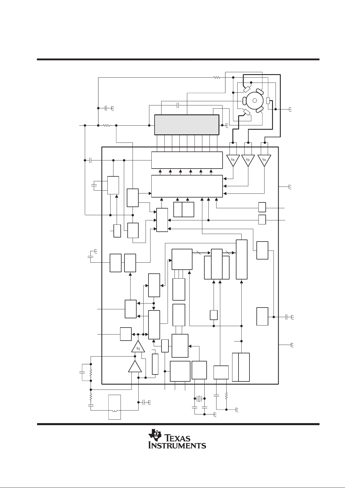
The TPIC43T01/02 is a monolithic motor control integrated circuit designed to provide RPM control to a 3-phase
brushless dc motor. The device provides two analog sensor input ports which include a speed sensor interface
and a Hall effect position interface. The speed feedback interface consists of an FG amplifier to receive an
external sinusoidal signal from a variable reluctance pickup and convert it to a digital speed signal for the control
circuit. When the motor speed is outside a ±5% window of the reference signal, an out-of-lock condition is
declared. The Hall ffect sensor input section receives low-level differential voltages from external naked Hall
elements and converts them to digital position reference signals for the control circuit for commutation control.
The core of the control circuit implements a digital signal processing algorithm consisting of a digital integrator
and filter with user adjustable parameters to optimize the closed loop performance of the control system. The
device contains an internal EEPROM to set integrator gain and digital filter coefficients. In addition, Texas
Instruments provides a PC based Windows compatible software package to input the motor and system
characteristics and convert them to control parameters for the TPIC43T01/02. The software generates a JEDEC
compatible file to program the device through a third party device programmer.
PRODUCTION DATA information is current as of publication date.
Products conform to specifications per the terms of Texas Instruments
standard warranty. Production processing does not necessarily include
testing of all parameters.
Please be aware that an important notice concerning availability, standard warranty, and use in critical applications of
Texas Instruments semiconductor products and disclaimers thereto appears at the end of this data sheet.
1
2
3
4
5
6
7
8
9
10
11
12
13
14
15
16
17
18
19
38
37
36
35
34
33
32
31
30
29
28
27
26
25
24
23
22
21
20
IN2+
IN2–
IN3+
IN3–
FGOUT
FGIN–
FGIN+
CLT
CT
RT
OSC2
OSC1
V
DD
FGSOUT
GND
LD
FSEL
S/S
F/R
IN1–
IN1+
TEST
V
PP
PHA
UGA
LGA
UGB
PHB
LGB
LGC
UGC
PHC
SENSE
CP2
CP1
V
CP
PGND
V
CC
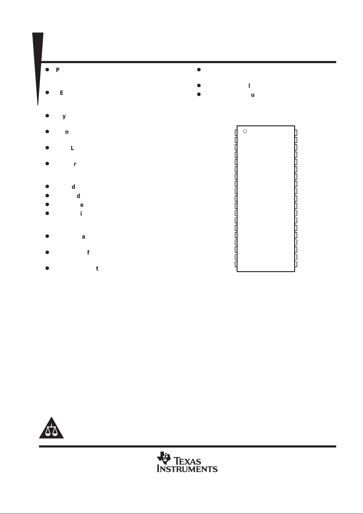
DA PACKAGE
(TOP VIEW)
Copyright 2000, Texas Instruments Incorporated
Windows is a trademark of Microsoft Corporation.
Page 2

TPIC43T01, TPIC43T02
THREE-PHASE BRUSHLESS MOTOR RPM CONTROLLERS
SLIS098 – APRIL 2000
2
POST OFFICE BOX 655303 • DALLAS, TEXAS 75265
description (continued)
The TPIC43T01/02 provides pre-drive outputs to control six external N-channel FET switches connected in a
3-half H-bridge configuration to drive a 3-phase dc motor. A companion TI Power+ Arrays device is available,
the TPIC1310 3-half H-bridge power array, to provide up to 2.5 A motor drive capability. The TPIC1310 is a
monolithic gate protected DMOS power array available in the TI 15-pin PowerFLEX power package. The
TPIC43T01/02 gate drive outputs are designed to also drive discrete N-channel power FETs.
The TPIC43T01/02 provides onboard supervisory and shutdown logic to protect the device and motor from fault
conditions. Oscillators, charge pump, and voltage regulators have been integrated into the TPIC43T01/02 to
minimize the number of external discrete components required to support the motor system.
Power+ Arrays and PowerFLEX are trademarks of Texas Instruments Incorporated.
Page 3
TPIC43T01, TPIC43T02
THREE-PHASE BRUSHLESS MOTOR RPM CONTROLLERS
SLIS098 – APRIL 2000
POST OFFICE BOX 655303 DALLAS, TEXAS 75265
• 3
A2
+
–
+
FGS
OUT
Lock
Detect
FGS Bias
VIN
÷ 2
Speed
Discrimination
EEPROM
Program
and Test
Logic
FG
Frequency
Select
FG Divide
Register 1
F0
F1
FG Ref
OSC
F
S
OSC
Freq Adj REG
5.8 MHz
OSC
Gain Select
Register
A0
A1
Digital
Integrator
OSC_INT
–
Digital
Filter
10
k2:3–Bit REG
k1:6–Bit REG
8
8–Bit PWM
Generator
÷
FILTCLK
F
S
Watchdog
Timer
Lock
OSC
Lock
Counter
Shutdown
Logic
÷ 32
Charge
Pump
CP
UVLO
Current
Limit
181 kHz
CPUV
OCSD
Gate Drive
Control and
Commutation
Logic
Sync
Rect
VDDUV S/S
PWM
S/S
F/R
ILIM
Pre-FET
Drivers
–
+
–
+
F/RS/S
V
DD
UVLO
5 V
VReg
OSC_INT
FGOUT FGSOUT LD CLT
V
CC
CP1 CP2
V
CP
SENSE
UGA
PHA
LGA
UGB
PHB
LGB
UGC
PHC
LGC
IN1+
IN1–
IN2+
IN2–
IN3+
IN3–
PGNDF/RS/SV
DD
GND
FGIN–
FGIN+
FSEL
V
PP
TEST
OSC1
OSC2
CT
RT
Power
Array
IC
3-Phase
Motor
Analog Hall-Effect
Position Sensors
CM = 22 µF
Rsense
0.2
CP = 0.01 µF
V
m
CS = 0.1–0.5 µF
CLT = 0.1 µF
150 pF
330 k
1 k
1 µF
Speed
Pickup
FG
0.01 µF
Cosc = 30 pF
Cosc = 30 pF
CT = 0.02 µF
RT = 12.5 k
1 µF
typical application
0.1 µF
1.5 k
Coast
Page 4

TPIC43T01, TPIC43T02
THREE-PHASE BRUSHLESS MOTOR RPM CONTROLLERS
SLIS098 – APRIL 2000
4
POST OFFICE BOX 655303 • DALLAS, TEXAS 75265
Terminal Functions
TERMINAL
NAME NO. I/O
DESCRIPTION
CLT 8 I Capacitor lock timer. CLT is a timing capacitor for the lock detect timer oscillator.
CP1 23 O Charge pump. CP1 is the switched capacitor output number 1.
CP2 24 O Charge pump. CP2 is the switched capacitor output number 2.
CT 9 I Timing capacitor. CT is the timing capacitor for the filter oscillator.
F/R 19 I Forward/Reverse. F/R is the forward/reverse direction data input.
FGIN– 6 I FGIN– is a inverting amplifier input.
FGIN+ 7 O FGIN+ is a noninverting amplifier input.
FGOUT 5 O FGOUT is a amplifier output.
FGSOUT 14 O FGSOUT is a buffered FGS comparator output.
FSEL 17 I Frequency select. FSEL is a frequency select input.
GND 15 Ground
IN1– 38 I Hall amplifier 1 inverting input
IN1+ 37 I Hall amplifier 1 noninverting input
IN2– 2 I Hall amplifier 2 inverting input
IN2+ 1 I Hall amplifier 2 noninverting input
IN3– 4 I Hall amplifier 3 inverting input
IN3+ 3 I Hall amplifier 3 non-inverting input
LD 16 O Lock Detect. LD is an active low, open-drain output.
LGA 32 I Lower gate drive A
LGB 29 I Lower gate drive B
LGC 28 I Lower gate drive C
OSC1 12 I Crystal oscillator input 1. OSC1 is an external OSC input.
OSC2 11 I Crystal oscillator input 2. OSC2 is an external OSC input.
PGND 21 PGND is the lower gate drive turnoff circuitry GND return.
PHA 34 I Phase A return
PHB 30 I Phase B return
PHC 26 I Phase C return
RT 10 O RT is the charge/discharge current setting resistor for filter and lock timer oscillators.
S/S 18 I Stop/Start. S/S = low to start.
SENSE 25 I Current limit sense. SENSE is the high-side current limit sense input.
TEST 36 I Test enable
UGA 33 I Upper gate drive A
UGB 31 I Upper gate drive B
UGC 27 I Upper gate drive C
V
CC
20 I Supply voltage
V
CP
22 O Charge-pump voltage source. VCP requires a storage capacitor.
V
DD
13 O 5 V Supply output
V
PP
35 I EEPROM programming voltage input
Page 5
TPIC43T01, TPIC43T02
THREE-PHASE BRUSHLESS MOTOR RPM CONTROLLERS
SLIS098 – APRIL 2000
5
POST OFFICE BOX 655303 • DALLAS, TEXAS 75265
absolute maximum ratings over the recommended operating case temperature range (unless
otherwise noted)
†
Supply voltage range, VCC (see Note 1) 8 V to 30 V. . . . . . . . . . . . . . . . . . . . . . . . . . . . . . . . . . . . . . . . . . . . . . . .
Motor drive voltage, V
(motor)
30 V. . . . . . . . . . . . . . . . . . . . . . . . . . . . . . . . . . . . . . . . . . . . . . . . . . . . . . . . . . . . . . . .
Charge pump output voltage, V
CP(max),
(V
CP
– VCC) V
CC
+ 20 V. . . . . . . . . . . . . . . . . . . . . . . . . . . . . . . . . . . .
Operating virtual junction temperature range, TJ 0°C to 150°C. . . . . . . . . . . . . . . . . . . . . . . . . . . . . . . . . . . . . . .
Thermal resistance, junction to ambient, R
θJA
121°C/W. . . . . . . . . . . . . . . . . . . . . . . . . . . . . . . . . . . . . . . . . . . . .
Storage temperature range, T
stg
–65°C to 150°C. . . . . . . . . . . . . . . . . . . . . . . . . . . . . . . . . . . . . . . . . . . . . . . . . . .
Lead temperature 1,6 mm (1/16 inch) from case for 10 seconds 260°C. . . . . . . . . . . . . . . . . . . . . . . . . . . . . . .
†
Stresses beyond those listed under “absolute maximum ratings” may cause permanent damage to the device. These are stress ratings only, and
functional operation of the device at these or any other conditions beyond those indicated under “recommended operating conditions” is not
implied. Exposure to absolute-maximum-rated conditions for extended periods may affect device reliability.
NOTE 1: The device will function, but may not meet all electrical specifications over this voltage range.
recommended operating conditions
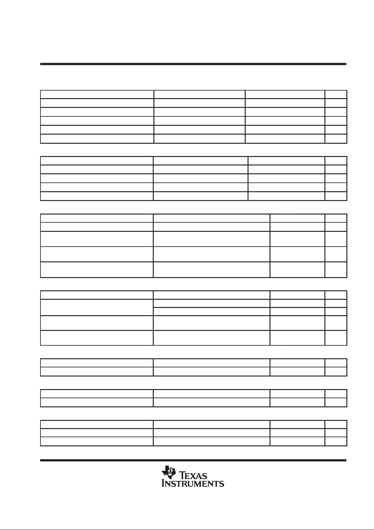
MIN TYP MAX UNIT
Supply voltage, V
CC
18 24 28 V
Extended supply voltage range, (see Note 1) 8 18 V
Operating case temperature, T
C
0 70 °C
NOTE 1: The device will function, but may not meet all electrical specifications over this voltage range.
EEPROM programming
MIN TYP MAX UNIT
VPP setup time, tsu(VPP) See Figure 20 2 µs
VPP pulse width duration, tw(VPP) See Figure 20 5 ms
VPP rise time, tr(VPP) See Figure 20 2 3 ms
VPP fall time, tf(VPP) See Figure 20 2 3 ms
electrical characteristics, TC = 25°C, V
CC
= 24V (unless otherwise noted)
PARAMETER TEST CONDITIONS MIN TYP MAX UNIT
S/S low, VCC = 28 V, I
(VCP)
= 2 mA
10 18
I
ccq
V
DD
quiescent current
S/S high, VCC = 28 V, I
(VCP)
= 0 mA
5 10
mA
VDD undervoltage lockout
PARAMETER TEST CONDITIONS MIN TYP MAX UNIT
V
DD(uvlo)
VDD under-voltage lockout threshold voltage 2.5 3.1 4 V
V
hys
VDD under-voltage lockout threshold voltage
hysteresis
1.1 V
5 V regulator
PARAMETER TEST CONDITIONS MIN TYP MAX UNIT
V
DD
Output voltage IO = –10 mA 4.75 5 5.25 V
V
(REGIN)
Line regulation VCC = 8 V to 28 V 0 50 mV
V
(REGOUT)
Load regulation IO = 0 to –10 mA 20 100 mV
Page 6
TPIC43T01, TPIC43T02
THREE-PHASE BRUSHLESS MOTOR RPM CONTROLLERS
SLIS098 – APRIL 2000
6
POST OFFICE BOX 655303 • DALLAS, TEXAS 75265
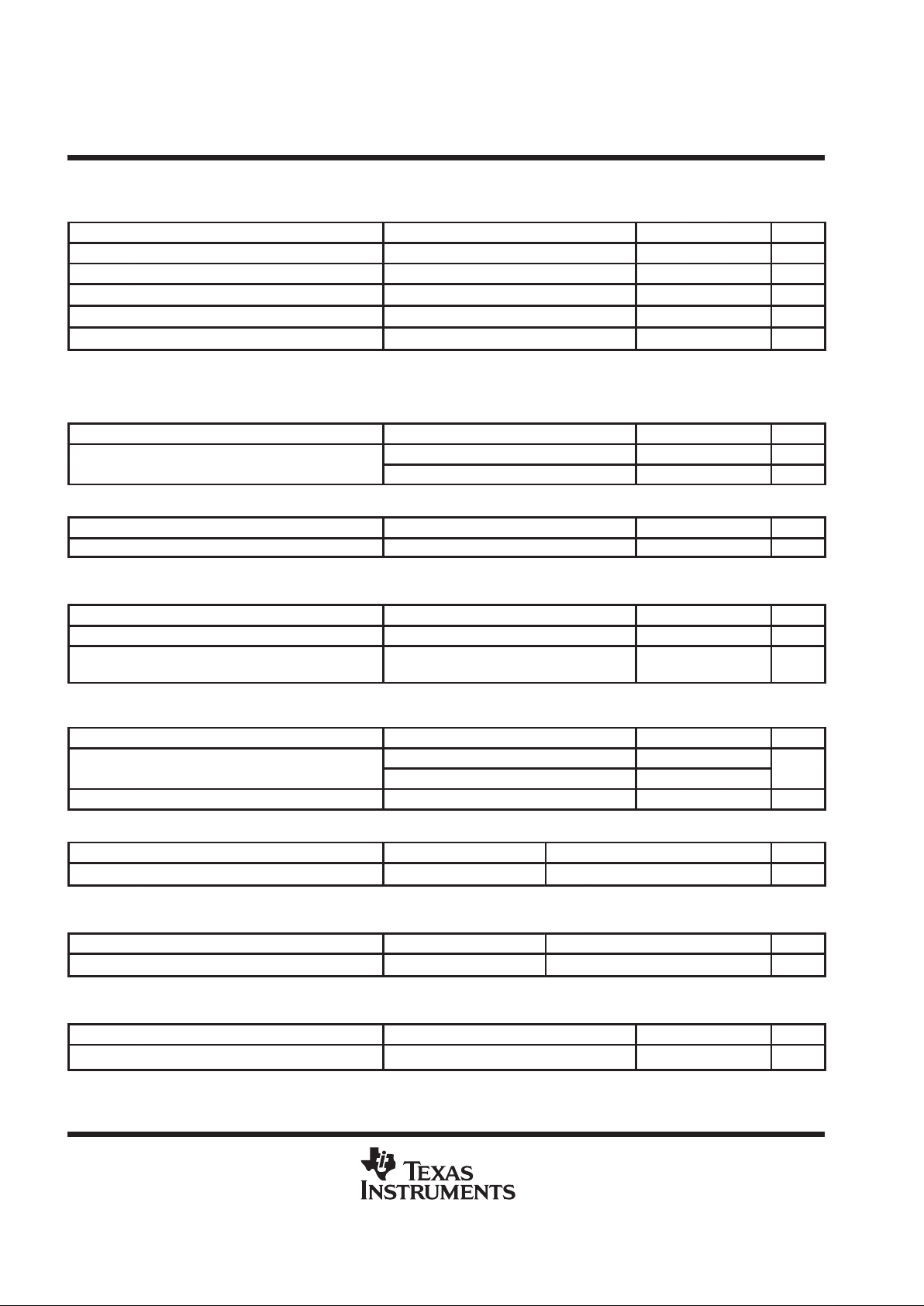
electrical characteristics, TC = 25°C, V
CC
= 24V (unless otherwise noted) (continued)
charge pump
PARAMETER TEST CONDITIONS MIN TYP MAX UNIT
p
IO = –1.5 mA, VCC = 18 V to 28 V,
CP = 0.01 µF, CS = 0.1 µF,
S/S = high
VCC + 14 VCC + 15 VCC + 17 V
V
O(CP)
Output voltage
IO = –1.5 mA, VCC = 8 V,
CP = 0.01 µF, CS = 0.1 µF,
S/S = high
VCC + 5.5 V
V
(CP–uvlo)
Under voltage lockout
IO = –1.5 mA, VCC = 8 V to 28 V,
S/S = high (VCP forced externally)
VCC + 5 VCC + 6 VCC + 7 V
V
hys(CP)
Under voltage lockout hysteresis
IO = –1.5 mA, VCC = 8 V to 28 V,
S/S = high (VCP forced externally)
0.6 V
FG signal conditioning
PARAMETER TEST CONDITIONS MIN TYP MAX UNIT
V
IO(FG)
Amplifier input offset voltage Measured at FGOUT 0.5 ±7 mV
I
IB(FG)
Amplifier input bias current Measured at FGIN– 0.02 ±1 µA
V
OH(FG)
Amplifier high level output voltage
I
(FG)
= –200 µA,
IDD = 0
VDD–500 mV VDD–350 mV V
V
OL(FG)
Amplifier low level output voltage I
(FG)
= 200 µA, IDD = 0 100 500 mV
A
V
Amplifier open-loop gain (see Note 2) 45 dB
V
(FGsens)
FG input sensitivity (see Note 2) 100 x Gain, at 2 kHz, 3 mV
V
(FGbias)
FG bias voltage IFG = 0 µA, IDD = 0 2.375 2.5 2.625 V
V
IT+(FGOUT)
FG comparator positive threshold
FGOUT with respect to
V
(FGIN+),
See Figure 8
215 250 285 mV
V
IO(FGOUT)
FG comparator offset voltage
FGOUT with respect to
V
(FGIN+)
, See Figure 8
0.8 ±7 mV
V
OL(FGSOUT)
FGSOUT open drain saturation voltage IO = 2 mA 0.4 0.7 V
I
lkg(FGSOUT)
FGSOUT leakage current VO = 5 V 0.08 10 µA
NOTE 2: Design target only. Not tested in production.
Hall sensor signal conditioning
PARAMETER TEST CONDITIONS MIN TYP MAX UNIT
I
IB(HL)
Input bias current (see Note 2) ±4 µA
V
ICR(HL)
Common-mode input voltage range (see Note 3) 1.5 3.5 V
V
IT+(HL)
Input positive threshold voltage
With respect to V
(CM)
, 1.5 kΩ in series
with both inputs, See Figure 9
4 8 12 mV
V
IT–(HL)
Input negative threshold voltage
With respect to VCM, 1.5 kΩ in series
with both inputs, See Figure 9
–4 –8 –12 mV
NOTES: 2. Design target only. Not tested in production.
3. Not measured, forced during testing.
FG reference crystal oscillator
PARAMETER TEST CONDITIONS MIN TYP MAX UNIT
V
IT+(OSC1)
OSC1 input upper threshold (see Note 3) 2.7 V
V
IT–(OSC1)
OSC1 input lower threshold (see Note 3) 1 V
NOTES: 3. Not measured, forced during testing.
Page 7
TPIC43T01, TPIC43T02
THREE-PHASE BRUSHLESS MOTOR RPM CONTROLLERS
SLIS098 – APRIL 2000
7
POST OFFICE BOX 655303 • DALLAS, TEXAS 75265
electrical characteristics, TC = 25°C, V
CC
= 24V (unless otherwise noted) (continued)
digital filter f
(s)
RC oscillator
PARAMETER TEST CONDITIONS MIN TYP MAX UNIT
V
ref(RT)
RT reference voltage I
(RT)
= –160 µA 0.19 V
DD
0.2 V
DD
0.21 V
DD
V
V
IT+(CT)
CT upper threshold voltage 0.7 V
DD
V
V
IT–(CT)
CT lower threshold voltage 0.3 V
DD
V
V
(CT)
CT amplitude 1.9 2 2.1 V
I
(CT)
CT charge/discharge current Measured at V
IT+(CT)
and V
IT–(CT)
1.8 I
(RT)
±2 I
(RT)
2.2 I
(RT)
A
lock detection timer
PARAMETER TEST CONDITIONS MIN TYP MAX UNIT
V
IT+(CLT)
CLT upper threshold voltage 0.7 V
DD
V
V
IT–(CLT)
CLT lower threshold voltage 0.3 V
DD
V
V
(CLT)
CLT amplitude 1.9 2 2.1 V
I
(CLT)
CLT charge/discharge current
Measured at VIT +
(CLT)
and V
IT–(CLT)
1.9 I
(RT)
±2 I
(RT)
2.3 I
(RT)
A
high side gate drive
PARAMETER TEST CONDITIONS MIN TYP MAX UNIT
V
C
Clamp voltage
UGX to PHX, I
(UGX)
= –100 µA
14 16 19 V
V
DS(UGX)
Source voltage drop
I
(UGX)
=–10 mA, VCP = VCC + 17 V,
Measure VCP – V
(UGX),VCC
= 18 V
1 1.2 V
Vsink
(UGX)
Sink voltage drop @10 mA
I
(UGX)
=10 mA, V
(PHx)
= 0,
Measure V
(UGX)
– V
(PHx) ,VCC
= 18 V
1.8 2 V
Vsink
(UGX)
Sink voltage drop @100 uA
I
(UGX)
=10 mA, V
(PHx)
= 0,
Measure V
(UGX)
– V
(PHx) ,VCC
= 18 V
0.56 0.7 V
low side gate drive
PARAMETER TEST CONDITIONS MIN TYP MAX UNIT
p
VCC = 18 to 28 V, I
(LGX)
= 0 14 16 19 V
V
O(REG15)
High level output voltage
VCC = 8 to 18 V, I
(LGX)
= 0 7.9 8 18 V
V
source(LGX)
Source voltage
I
(LGX)
= –10 mA, with respect to PGND,
VCC = 18 V
12 14.5 V
V
DS(LGX)
Sink voltage drop
I
(LGX)
= 10 mA, with respect to PGND,
VCC = 18 V
0.6 1 V
current limit control
PARAMETER TEST CONDITIONS MIN TYP MAX UNIT
V
IT(lim)
Limit threshold voltage VCC – V
(SENSE)
0.46 0.5 0.54 V
over-current shutdown control
PARAMETER TEST CONDITIONS MIN TYP MAX UNIT
V
IT(ocsd)
Detection threshold voltage VCC – V
(SENSE)
0.9 1 1.1 V
EEPROM programming
PARAMETER TEST CONDITIONS MIN TYP MAX UNIT
V
PP
VPP programming voltage 12 13 15 V
R
(VPP)
VPP pulldown resistance VPP = 1 V 15 23 35 kΩ
Page 8
TPIC43T01, TPIC43T02
THREE-PHASE BRUSHLESS MOTOR RPM CONTROLLERS
SLIS098 – APRIL 2000
8
POST OFFICE BOX 655303 • DALLAS, TEXAS 75265
electrical characteristics, TC = 25°C, V
CC
= 24V (unless otherwise noted) (continued)
digital input pins
PARAMETER TEST CONDITIONS MIN TYP MAX UNIT
V
IH
Digital input high level input voltage Interface from 3.3 V controller 2.2 V
V
IL
Digital input low level input voltage Interface from 3.3 V controller 1.1 V
I
(pullup)
Digital input pullup current, S/S, FSEL VIN = 2.2 V –9 –14 –18 µA
I
(F/R)
Digital input pulldown current, F/R VIN = 1.1 V 17.5 27 35 µA
I
(TEST)
TEST input pulldown current VIN = 1.1 V 130 200 250 µA
switching characteristics, T
C
= 25°C, VCC = 24 V
charge pump
PARAMETER TEST CONDITIONS MIN TYP MAX UNIT
180 kHz
f
(CP)
Switching frequenc
y
TC = 0 to 70°C 140 220 kHz
FG signal conditioning
PARAMETER TEST CONDITIONS MIN TYP MAX UNIT
BW Gain bandwidth (see Note 2) 200 kHz
NOTE 2. Design target only. Not tested in production.
FG reference crystal oscillator
PARAMETER TEST CONDITIONS MIN TYP MAX UNIT
f
(OSC)
Crystal frequency range (see Note 2) 5 6.87 10 MHz
f
(OSC1)
OSC1 frequency range
OSC1 driven externally, see FG Reference
Oscillator section
1 10 MHz
NOTE 2. Design target only. Not tested in production.
PWM control
PARAMETER TEST CONDITIONS MIN TYP MAX UNIT
22.7
f
(PWM)
PWM frequenc
y
TC = 0 to 70°C
18 27
kH
z
t
(DT)
Gate drive dead time control See Figure 3 1 3.2 µs
digital filter f
(s)
RC oscillator
PARAMETER TEST CONDITIONS MIN TYP MAX UNIT
f
(CT)
Oscillator frequency (see Note 2) 1/(2 × RT × CT) ±10% Hz
NOTE 2. Design target only. Not tested in production.
lock detection timer
PARAMETER TEST CONDITIONS MIN TYP MAX UNIT
f
(CLT)
CLT oscillator frequency (see Note 2) 1/(2 × RT × CLT) ±10% Hz
NOTE 2. Design target only. Not tested in production.
lock detection
PARAMETER TEST CONDITIONS MIN TYP MAX UNIT
LD
ERR
†
Lock detect threshold ±5 %
†
Non JEDEC symbol.
Page 9
TPIC43T01, TPIC43T02
THREE-PHASE BRUSHLESS MOTOR RPM CONTROLLERS
SLIS098 – APRIL 2000
9
POST OFFICE BOX 655303 • DALLAS, TEXAS 75265
switching characteristics, T
C
= 25°C, VCC = 24 V (continued)
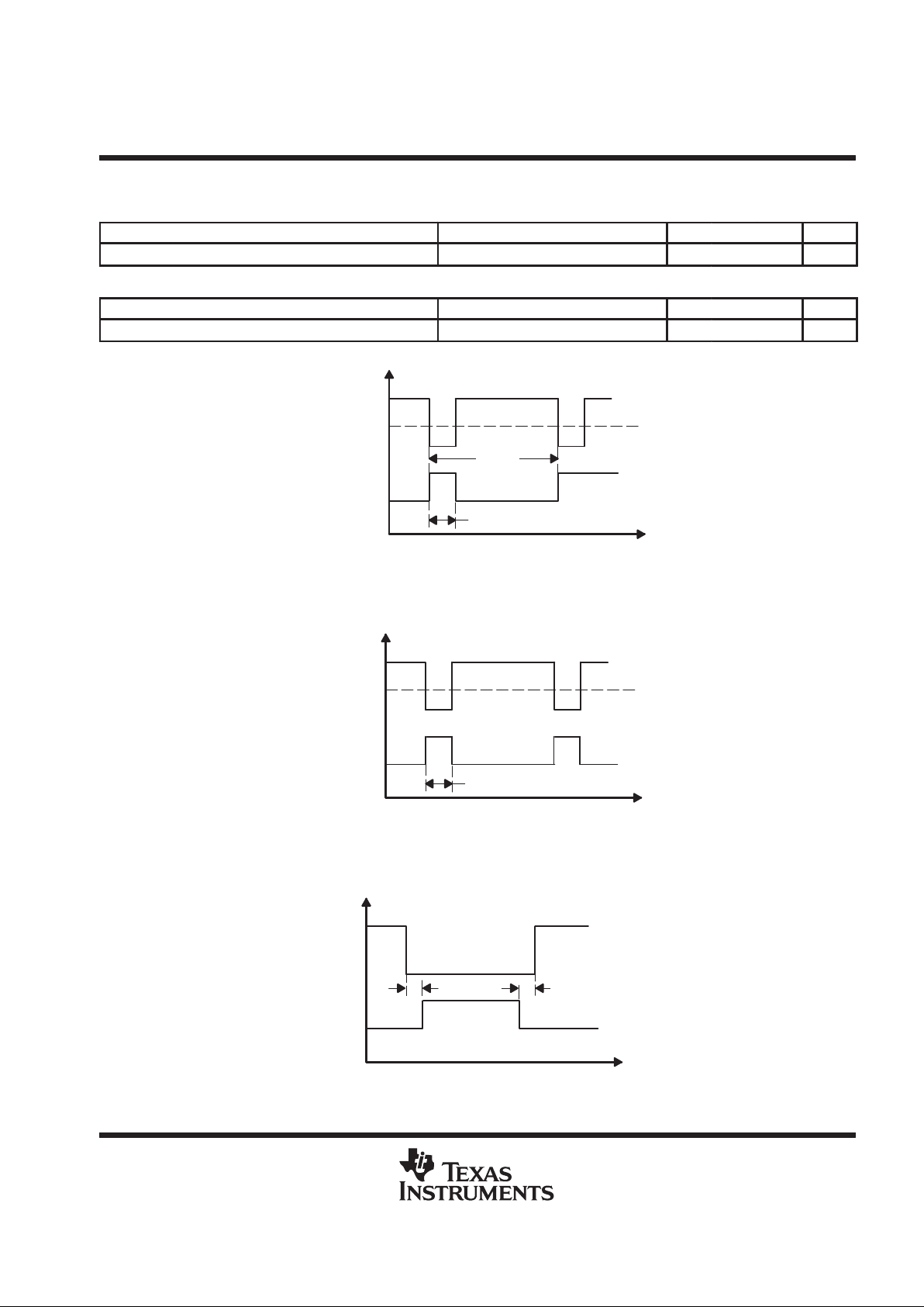
current limit control
PARAMETER TEST CONDITIONS MIN TYP MAX UNIT
t
(DG)
Deglitch blanking time V
(SENSE)
– VL ≥ 100 mV, See Figure 1 0.5 3.7 6.5 µs
over-current shutdown control
PARAMETER TEST CONDITIONS MIN TYP MAX UNIT
t
(OCSD)
Response time See Figure 2 0.5 1.5 2.5 µs
High-Side Gate
Output
PWM
Cycle
t
(DG)
Amplitude
time
V
CC
V
L
V
(SENSE)
Figure 1. Current Limit Deglitch Blanking Time
High-Side Gate
Output
t
(OCSD)
Amplitude
time
V
CC
V
OCSD
V
(SENSE)
Figure 2. Over-Current Shutdown Response Time
Amplitude
time
UGx
t
(DT)
LGx
t
(DT)
Figure 3. Gate Drive Deadtime
Page 10

TPIC43T01, TPIC43T02
THREE-PHASE BRUSHLESS MOTOR RPM CONTROLLERS
SLIS098 – APRIL 2000
10
POST OFFICE BOX 655303 • DALLAS, TEXAS 75265
PRINCIPLES OF OPERATION
voltage regulator
The TPIC43T01/02 receives an 8 to 28 V supply voltage at the VCC pin and generates an internal 5 V, V
DD,
supply for the internal analog and digital logic. An external terminal for VDD is provided for a required external
1 µF compensation capacitor. The regulator can also supply up to 10 mA current from the VDD pin to external
circuitry .
oscillators
internal oscillator
The device generates an internal 5.8 MHz clock to supply a frequency input to internal control blocks as
presented in Figure 4. No external components are required.
5.8 MHz
Oscillator
÷ 32
Charge
Pump
ILIM/OCSD
Deglitch
Timer
8-Bit PWM
Generator
PWM, f∼23 kHz
Watchdog
÷ 8
Gate Drive
Dead Time
Control
Integrator
181 kHz
∼ 45 kHz
Figure 4. 5.8 MHz Internal Oscillator Fanout
FG reference oscillator
The FG reference oscillator provides a clock to the FG frequency control section of the device. The oscillator
requires an external 5 to 10 MHz crystal to select the primary frequency. The user can alternatively input a 1
to 10 MHz signal from a signal generator to the OSC1 input to replace the external crystal. Two EEPROM bits
allow programming four different crystal oscillator divide-by values for controlling the FG reference frequency .
The FSEL pin provides an additional divide-by-2 for on-the-fly FG frequency (RPM) selection. Table 1 shows
the divide-by count and resulting FG reference frequency based on the two EEPROM bits (address 1, bits 0–1)
and the FSEL pin input level.
Page 11

TPIC43T01, TPIC43T02
THREE-PHASE BRUSHLESS MOTOR RPM CONTROLLERS
SLIS098 – APRIL 2000
11
POST OFFICE BOX 655303 • DALLAS, TEXAS 75265
PRINCIPLES OF OPERATION
Table 1. FG Reference Frequency
EEPROM EEPROM FSEL PRE-DIVIDER TOTAL f
FG f
(ref)
@f
(osc)
ADDR 1, BIT 1 ADDR 1, BIT 0 INPUT DIVIDE BY
(osc)
DIVIDE-BY
1 MHZ 5 MHZ 10 MHZ
0 0 1 3 3072 326 1628 3256
0 0 0 6 6144 163 814 1628
0 1 1 4 4096 244 1221 2441
0 1 0 8 8192 122 610 1221
1 0 1 6 6144 163 814 1628
1 0 0 12 12,288 81 407 814
1 1 1 8
8192
†
122 610 1221
1 1 0 16
16,384
†
61 305 610
†
Equals default value
sampling frequency for the digital filter, f
(s)
, oscillator
An external resistor (RT) and capacitor (CT) must be connected from the respective RT and CT terminals to
GND to set the sampling frequency for the digital filter. Charge/discharge current at terminal CT will nominally
be ±2 × (1V/RT). Nominal period is determined by the formula: T
(CT)
= 2 × RT × CT (see Figure 5).
_
+
_
+
V
DD
I
(RT)
2I
(RT)
I
RT
RT
RTV
(RT)
= 1 V
CT
CT
_
+
1.5
3.5
R
S
Q
Clock To
Digital Filter
4I
(RT)
4:1
1:2
1:1
V
DD
1 V Internal
Reference
I
(RT)
Figure 5. Digital Filter Sampling Clock Generation
Page 12

TPIC43T01, TPIC43T02
THREE-PHASE BRUSHLESS MOTOR RPM CONTROLLERS
SLIS098 – APRIL 2000
12
POST OFFICE BOX 655303 • DALLAS, TEXAS 75265
PRINCIPLES OF OPERATION
lock timer oscillator/counter
Overall lock timer functionality is implemented by the combination of the oscillator and counter. The lock timer
oscillator is identical to the sampling frequency oscillator. The external resistor (RT) is used as the current
setting reference for both blocks. An external capacitor must be connected from the CLT terminal to GND to
set the period, T
(CLT)
, of the lock timer oscillator. The nominal period is determined by the formula:
T
CLT
= 2 × RT × CLT. When an out-of-lock signal is generated by the lock detect block (see lock detect section),
the lock timer counter will count at the frequency of the lock timer oscillator. Should the out-of-lock signal remain
for the duration of the counter completing 1023 counts, a lock timer time-out signal will then be generated which
the shutdown logic block will respond to (see shutdown section). The lock timer time-out is thus set by
T
CLT
× 1023.
power-up clear
An under-voltage lockout and power-up clear are provided to ensure FET drive outputs are set to a known state
during power-up. The device is held in a CLEAR state until the following three conditions are met:
1. VDD > V
DD(uvlo)
, after which a power-up clear (PUC) time will begin.
2. The PUC timer counts 3 cycles of internal 20 kHz signal (internal 5.8 MHz ÷ 255), or ≅ 132 µs.
3. The charge pump voltage, V
(CP)
, has charged to at least VCC + 5 V.
shutdown
The scheme for shutdown includes monitoring two conditions and latching the device in a CLEAR state should
an abnormal condition occur. Once shutdown is latched, the S/S input must be cycled high then low, or power
cycled OFF then ON to release shutdown and resume normal operation. If an abnormal condition still exists after
the S/S pin has been cycled, the device will relatch shutdown. A 1 on either S/S or V
DD
pins will clear the lock
timer. A VDD under-voltage-lockout detect will force a global clear. (see Table 2 and Figure 6).
Table 2. Shutdown Conditions
LATCHED SHUTDOWN
CONDITIONS
UNLATCHED SHUTDOWN CONDITIONS S/S
INTERNAL
LT
GATE
OCSD LT CP UV VDD UVLO INPUT
CLR
LTCLR
OUTPUTS
X X X X H 0 0 0
X X X
VDD < V
DD(uvlo)
X 0 0 0
V
(SENSE)
< V
(OCSD)
Out of
Lock < t
(LT)
V
O(CP)
> V
(CPUV)VDD
> V
DD(uvlo)
+ 3 counts H↓L 1 1 1
X X
VCP < V
(CPUV)
for > t
(DG)
X X X X 0
V
(SENSE)
> V
(OCSD)
for > t
(DG)
X X X X X X 0
X
Out of
Lock > t
(LT)
X X L X 1 0
Page 13

TPIC43T01, TPIC43T02
THREE-PHASE BRUSHLESS MOTOR RPM CONTROLLERS
SLIS098 – APRIL 2000
13
POST OFFICE BOX 655303 • DALLAS, TEXAS 75265
PRINCIPLES OF OPERATION
V
DD
UVLO
3 Counts
PUC
S/S
Internal
5.8 MHz
OSC
÷ 32
Charge Pump
UV
t
(DG)
PWM
(22 KHz)
CPUV
D Q
Q
CLR
ENA
Shutdown
Latch
V
DD
OSC
Lock
OSC
Lock
Detect
Lock
Counter
LTCLR
ILIM
OCSD
OCSD
LT
ENA
ENA
CLR
t
(DG)
Figure 6. Shutdown Logic Block Diagram
FG amplifier
The FG amplifier amplifies the ac signal from the FG variable-reluctance pickup and converts it to a digital signal
for internal use in the FG frequency control loop (see Figure 7). Figure 8 illustrates the generation of the
FGSOUT signal in the FG amplifier section. Two comparators driving an RS latch are used with the upper
comparator threshold (taken from the 5 V VDD band-gap buffer circuit feedback resistor string), while the lower
comparator threshold is connected to the FG bias voltage. This provides controlled hysteresis above the FGIN+
amplifier input reference voltage and zero-crossing detection at the input reference voltage.
_
+
_
+
R
S
Q
FG
Comparator
_
+
FGS Buffer
FG Amp
_
+
1/2 V
DD
+ 180 mV
1/2 V
DD
Band-Gap
Buffer
OP-Amp
FGSOUT
FGOUT
FGIN–
FGIN+
330 kΩ
1 kΩ
1 µF
FG
Winding
150 pF
Figure 7. FG Signal Conditioning Schematic
Page 14

TPIC43T01, TPIC43T02
THREE-PHASE BRUSHLESS MOTOR RPM CONTROLLERS
SLIS098 – APRIL 2000
14
POST OFFICE BOX 655303 • DALLAS, TEXAS 75265
PRINCIPLES OF OPERATION
V
IT+(FGOUT)
V
IO+(FGOUT)
FGOUT
V
(FGIN+)
FGSOUT
Figure 8. FG Signal Conditioning Block Waveforms
lock detect
The lock detect circuit monitors FGSOUT and flags when it is within ±5% of f
(ref)
. The circuit counts the number
of FG reference clocks which occur between the rising edges of FGSOUT to determine whether motor speed
has reached the locking range. When a lock occurs, the LD terminal transitions low. When the FGSOUT
frequency is not within the ±5% of f
(ref)
window, an internal
out-of-lock
signal is generated for the lock timer block
(see
lock timer
section).
Hall signal conditioning
The Hall signal conditioning block receives the low-level differential voltage from naked Hall elements and
implements symmetric threshold detection and hysteresis for noise rejection. The circuit has nominal input
voltage thresholds of ±7 mV at the INx+ pin with respect to the INx– pin. The common-mode input voltage range
is 1.5 V to 3.5 V (see Figure 9).
V
IT+(HL)
V
IT–(HL)
V
(Hall)
(INx+)
V
(CM)
(INx–)
Hall Amp
Output
(Internal)
Figure 9. Hall Signal Conditioning Waveforms
Page 15

TPIC43T01, TPIC43T02
THREE-PHASE BRUSHLESS MOTOR RPM CONTROLLERS
SLIS098 – APRIL 2000
15
POST OFFICE BOX 655303 • DALLAS, TEXAS 75265
PRINCIPLES OF OPERATION
rotor position sensing/commutation control
T o electronically commutate the three phases, the state of the three Hall-ef fect sensors is decoded to drive the
correct phases based on desired motor rotational direction and rotor position. This is accomplished by decoding
the Hall sensor gray-code with the F/R input condition as described in T able 3. If all three Hall inputs are detected
as identical states, this is an illegal condition and the device turns all outputs OFF.
Table 3. Hall Position Sensor Input Gray-Code Logic
COMMUTATION F/R = LOW F/R = HIGH PHASE A PHASE B PHASE C
STEP IN1 IN2 IN3 IN1 IN2 IN3 UPPER LOWER UPPER LOWER UPPER LOWER
A L L H H H L PWM Note 4 ON
B L H H H L L PWM Note 4 ON
C L H L H L H PWM Note 4 ON
D H H L L L H ON PWM Note 4
E H L L L H H ON PWM Note 4
F H L H L H L ON PWM Note 4
Illegal L L L L L L all OFF
Illegal H H H H H H all OFF
NOTE 4: For the Half-H in which GUx is being switched by PWM, the complimentary LGx can be EEPROM programmed by a single bit to enable
or disable synchronous rectification during t
(OFF)
of each PWM cycle. This allows configuration of the device for applications where
synchronous rectification can or cannot be used.
digital PWM operation
In Table 3, the term PWM represents the pulse-width-modulation duty-cycle. PWM switching is implemented
with the upper gate drive such that recirculation occurs in the lower external FET during the OFF portion of each
period. Coast mode is enabled or disabled using EEPROM address 0, bit 4. Synchronous rectification mode
is enabled or disabled using EEPROM address 0, bit 3.
An 8-bit digital PWM circuit uses an internal 5.8 Mhz oscillator as an input frequency. Each PWM period is
defined by 255 (28 –1) intervals where the number of ON intervals is controlled by the value of an 8-bit binary
input word from the digital filter output. The PWM generator is implemented such that duty cycle is:
Duty cycle
+
n
ǒ
28–1
Ǔ
+
n
255
Where:
n = decimal equivalent of the 8-bit binary input word
coast mode, (EEPROM address 0, bit 4, default = H)
When coast function is enabled (EEPROM address 0, bit 4 = H), the device uses a special mode to control speed
of the motor when it exceeds the selected reference speed. Referring to Figure 10, when FGSOUT frequency
exceeds f
(ref)
by 5%, resulting in a loss of lock detect, the high-side FET gate drives (UGx) are disabled and the
low-side FET drives (LGx) continue to sequence as per the commutation table. This will continue until FGSOUT
frequency drops below f
(ref)
, which re-enables the high-side gate drives. The coast mode will override
synchronous rectification mode if both are enabled (see following) after the FSGOUT signal exceeds f
(ref)
.
Page 16

TPIC43T01, TPIC43T02
THREE-PHASE BRUSHLESS MOTOR RPM CONTROLLERS
SLIS098 – APRIL 2000
16
POST OFFICE BOX 655303 • DALLAS, TEXAS 75265
PRINCIPLES OF OPERATION
Coast
Lock Detect
Range
f
(FGSOUT)
(Motor RPM)
+5%
f
(ref)
–5%
Figure 10. Coast Mode Operation
synchronous rectification mode (EEPROM address 0, bit 3, default = H for TPIC43T01, default = L for
TPIC43T02)
The TPIC43T01 is set up with synchronous rectification enabled. With synchronous rectification enabled
(EEPROM address 0, bit 3 = H), the complimentary LGx of the phase being pulse-width-modulated will turn ON
inversely to UGx during each PWM cycle. This provides a low resistance path through the low-side FET,
operating in inverse, for recirculating inductive current of the motor winding. This technique improves drive
efficiency over allowing the inductive energy to recirculate through the FET’s drain-body diode. Dead-time will
be controlled in each half-H between upper to lower and lower to upper transitions to prevent high current
conduction directly through the power FET s. During this dead-time, recirculation current, due to load inductance,
will occur in the lower FET body diode. After dead-time, the complimentary LGx will be turned on, thus reducing
power dissipation by using the lower FET in inverse to produce a lower voltage drop across
r
DS(ON)
than would
occur across VF of the FET drain-body diode (see Figure 11).
Sync Blanking
f
(FG)
(Motor RPM)
+5%
f
ref
–5%
Synchronous
Rectification
Synchronous
Rectification
Lock Detect
Range
Figure 11. Synchronous Rectification/Coast Mode Operation
The TPIC43T02 is set up with synchronous rectification disabled. With synchronous rectification disabled
(EEPROM address 0, bit 3 = L), the complimentary LGx will stay low during the OFF time of UGx, and inductive
current will thus recirculate through the lower external FET drain-body diode for the duration of t
(OFF)
.
Page 17

TPIC43T01, TPIC43T02
THREE-PHASE BRUSHLESS MOTOR RPM CONTROLLERS
SLIS098 – APRIL 2000
17
POST OFFICE BOX 655303 • DALLAS, TEXAS 75265
PRINCIPLES OF OPERATION
digital integrator gain selections
In Table 4, EEPROM bits can be set for different clocking rates of the digital integrator. In effect, this allows for
different integrator gain, thereby allowing the user to optimize loop performance (see Figure 12). The integrator
circuit actually utilizes 14 bits with a 4-bit pre-integrator prior to the 10 bits which are output to the digital filter.
This design increases resolution in the error detected by the speed discriminator while reducing the bit-count
output to the digital filter.
Table 4. Digital Integrator Gain Selection Table
EEPROM
ADDR 0
BIT 2
EEPROM
ADDR 0
BIT 1
EEPROM
ADDR 0
BIT 0
INTEGRATOR INPUT
FREQUENCY DIVIDE
DOWN
INTEGRATOR
GAIN ADJUST
TYPICAL INTEGRATOR
INPUT FREQUENCY
0 0 0 ÷ 1
†
0 dB 5.8 MHz
0 1 0 ÷ 2 –6 dB 2.9 MHz
0 0 1 ÷ 3 –9.5 dB 1.93 MHz
1 0 0 ÷ 4 –12 dB 1.45 MHz
0 1 1 ÷ 6 –15.5 dB 967 kHz
1 1 0 ÷ 8 –18 dB 725 kHz
1 0 1 ÷ 12 –21.5 dB 483 kHz
1 1 1 ÷ 16 –24 dB 363 kHz
†
Default setting for integrator clock.
Pre-
Integrator
(4 Bits)
Integrator
(10 Bits)
Digital
Filter
8-Bit
PWM
Generator
Divide-By
Gain
Adjust
Input Frequency
B0
B1
B2
5.8 MHz
OSC
Up
Down
Figure 12. Integrator Implementation
Page 18

TPIC43T01, TPIC43T02
THREE-PHASE BRUSHLESS MOTOR RPM CONTROLLERS
SLIS098 – APRIL 2000
18
POST OFFICE BOX 655303 • DALLAS, TEXAS 75265
PRINCIPLES OF OPERATION
digital filter coefficients
The two digital filter coefficients can be set by programming the EEPROM to select the pole and zero for the
digital filter. The pole and zero values are directly proportional to the digital filter sample rate, T
(s)
, and the filter
gain is independent of T
(s)
. The adjustment range of T
(s)
is from 250 µs to 1 ms (see Figure 13). The K1 lead
coefficient value is stored in bits 2–7 of Address 1 as a BCD equivalent of the K1 coefficient. K1 has a range
from 0 to 63, with a default setting of 28. See Table 5 for a typical range of pole and zero frequencies at
T
(s)
= 500 µs. The K2 coefficient value is stored in bits 5–7 of Address 0 (see Table 6 and Figure 14).
The gain of the digital filter is given by the equation:
OUT
+
IN [128 Z–K2] 0.25
Z–K1ń128
Where:
Z represents a delay of one period of the f
(s)
sampling clock.
The scaling factor of 0.25 in the above equation accounts for the difference in word lengths in the integrator
(10 bits), the filter (17 bits) and the PWM generator (8 bits).
Digital
Integrator
(10-Bit Data Word)
Σ
+
+
1/Z
Σ
–
K1
K2
+
PWM
Generator
(8-Bit Data Word)
Figure 13. Digital Filter System Diagram
Table 5. Filter Zero and Gain as a Function of K2, Ts = 500 µs
K1 = 14 (POLE = 704 Hz) K1 = 28 (POLE = 483 Hz) K1 = 56 (POLE = 263 Hz)
K2
ZERO (Hz) GAIN ZERO (Hz) GAIN ZERO (Hz) GAIN
127 6.2 0.28 4.8 0.32 3.7 0.45
126 12.4 0.28 9.7 0.32 7.3 0.45
125 18.4 0.42 14.5 0.48 11 0.68
124 24.7 0.28 19.3 0.32 14.6 0.45
123 30.9 0.35 24.2 0.4 18.3 0.56
122 37.1 0.42 29 0.48 21.9 0.68
121 43.3 0.25 33.9 0.28 25.6 0.39
120 49.4 0.28 38.7 0.32 29.2 0.45
Page 19

TPIC43T01, TPIC43T02
THREE-PHASE BRUSHLESS MOTOR RPM CONTROLLERS
SLIS098 – APRIL 2000
19
POST OFFICE BOX 655303 • DALLAS, TEXAS 75265
PRINCIPLES OF OPERATION
Table 6. Digital Coefficient Truth Table
EEPROM
ADDR 0
BIT 7
EEPROM
ADDR 0
BIT 6
EEPROM
ADDR 0
BIT 5
K2
COEFFICIENT
0 0 0 120
0 0 1 121
0 1 0 122
0 1 1 123
1 0 0 124
†
1 0 1 125
1 1 0 126
1 1 1 127
†
Default setting for the digital filter coefficient
15
5
40
0
120 121 122 123 124
Digital Filter Zero – Hz
30
20
35
K2 and K1 Filter Coefficient
50
125 126 127
45
25
10
Default Zero Setting
K1 = 14
K1 = 28
K1 = 56
DIGITAL FILTER ZERO
vs
K2 and K1 FILTER COEFFICIENT, (T
S
= 500 µs)
Figure 14. Digital Filter Coefficient
FG watchdog
The FG watchdog monitors FGOUT output, allowing an internal timer to count until a transition in FGOUT occurs
and clears the counter. Should timer time-out occur by reaching a count equivalent to 25 ms (512 counts of the
PWM clock), two actions are taken: 1) speed discriminator UP error output is set to 100%; 2) lock detect is set
and lock timer begins counting (see
lock timer oscillator/counter
section). These actions ensure the digital
integrator counts up (increasing motor drive PWM) at startup of the system, or, if the FG signal is lost during
operation and if no detection of an FG period of < 25 ms occurs for the duration of the lock timer, the IC will go
into shutdown mode, disabling the motor drive (see
shutdown
section).
Page 20

TPIC43T01, TPIC43T02
THREE-PHASE BRUSHLESS MOTOR RPM CONTROLLERS
SLIS098 – APRIL 2000
20
POST OFFICE BOX 655303 • DALLAS, TEXAS 75265
PRINCIPLES OF OPERATION
current limit/over-current shutdown
Referring to Figure 15, two comparators monitor the voltage drop across an external current sensing resistor,
R
(SENSE)
. The sensed voltage, V
(SENSE)
, is then compared against two VCC referred voltages, VL and V
(OCSD)
.
When V
(SENSE)
exceeds VL, the ILIM comparator outputs a high level. When V
(SENSE)
exceeds V
(OCSD)
, the
OCSD comparator also outputs a high level. The combination of these two comparator outputs is then used in
conjunction with a deglitch or blanking timer to discriminate between a high di/dt, short-duration current spike.
This spike is commonly caused by reverse recover time (t
rr
) current at the start of each PWM cycle and a portion
of the current waveform with lower di/dt. The lower di/dt is controlled by the L/R time constant of the motor
winding (see Figure 16). A comparator is also used to detect over current conditions caused by a shorted-load
or shorted phase-winding to GND (see Figure 17).
QD
Q CLK
CLR
_
+
_
+
V
(LM)
V
OCSD
OCSD
COMP
ILIM
COMP
R
2 × R
Digital
Deglitch
(0.5–2 µs)
PWM
Control
IDET
_
+
V
DD
V
ref
V
(thres)
Generation
ILIMIT
Block
OCSD
S/S
PWM_OFF
PWM_START
OSC
V
CC
Power
Drivers
SENSE
V
(sense)
R
(sense)
+
A
C
B
3-Phase
Motor
Figure 15. ILIMIT/OCSD Diagram
Page 21

TPIC43T01, TPIC43T02
THREE-PHASE BRUSHLESS MOTOR RPM CONTROLLERS
SLIS098 – APRIL 2000
21
POST OFFICE BOX 655303 • DALLAS, TEXAS 75265
PRINCIPLES OF OPERATION
current limit/over-current shutdown (continued)
The deglitch timer prevents the ILIM COMP high from being recognized unless it occurs for the duration of the
timer, after which a high IDET level occurs. This IDET level is used to terminate, or latch of f the upper gate drive
being driven by PWM for the remainder of the PWM interval. This ILIM latch and deglitch timer clears at the start
of each new PWM cycle; thus, a cycle-by-cycle PWM controlled current limit is implemented.
Current spike from trr
t
(DG)
= 0.5 to 6.5 µs
t
(DE-GLITCH)
Amplitude
V
OCSD
V
L
VCC – VSENSE
time
ILIM
COMP
IDET
OCSD
COMP
OCSD
Figure 16. Normal Motor Current Waveform With trr Spike at Start of PWM Cycle
Amplitude
High Ipeak from shorted phase winding
or shorted-phase-to-GND(> 5 A depending on the value of R
(SENSE)
)
V
OCSD
V
L
VCC – VSENSE
t
(ocsd)
= 0.5 to 2.5 µs
Combination of IDET high and OCSDCOMP high
sets OSCD latch
Latches high until S/S cycles
time
Figure 17. Motor Current Waveform With Shorted Phase W inding or Shorted Phase to GND
Page 22

TPIC43T01, TPIC43T02
THREE-PHASE BRUSHLESS MOTOR RPM CONTROLLERS
SLIS098 – APRIL 2000
22
POST OFFICE BOX 655303 • DALLAS, TEXAS 75265
PRINCIPLES OF OPERATION
EEPROM registers
There are two user configurable EEPROM bit registers accessible through the serial test interface when the
device is configured in TEST mode. This mode is enabled when the TEST pin is held high at 5 V . Once the device
is placed in TEST mode, either register can be programmed by transmitting a 16-bit word. The first three bits
of this transmission are the address and R/W for the register the user wishes to modify . The next five bits must
be held low, and the remaining eight bits are configuration bits. Each register must be programmed
independently, i.e. once the register value is written, the V
PP
pin must immediately be taken to 13.5 V in the
manner described in the
EEPROM Programming
section. The two EEPROM registers are summarized in
Table 7. A detailed definition outlining the function of each bit in the EEPROM is presented in the respective
functional description sections of this specification (see Notes 5 and 6).
Table 7. EEPROM Register Definition
EEPROM REGISTER CONFIGURATION BITS
ADDR
BIT 7 BIT 6 BIT 5 BIT 4 BIT 3 BIT 2 BIT 1 BIT 0
0 K2 Coefficient Coast Enable
Synchronous
Rectification
Integrator Gain Select
TPIC43T01 default 1 0 0 1 1 0 0 0
TPIC43T02 default 1 0 0 1 0 0 0 0
1 K1 Coefficient FG Frequency Select
TPIC43T01 default 0 1 1 1 0 0 1 1
TPIC43T02 default 0 1 1 1 0 0 1 1
NOTES: 5. Bit 0 in the EEPROM register definition table corresponds to D0 and E0 in the serial protocol sequence.
6. Data read out of the EEPROM corresponds to the contents of the register at the time it is read. (A register can
be read after programming it in order to verify that the EEPROM was programmed properly.)
serial test interface
User-programmable functions are controlled using two 16-bit EEPROM registers. These registers are
programmed by placing the device in program/test mode by pulling the TEST pin high and transferring data
using the serial interface. Pins 14 and 17–19 are multipurpose pins, which are configured for serial test mode
when the TEST pin is high (see Table 8).
Table 8. Serial Test Interface Pin Definition
PIN
NAME NO.
PIN DESCRIPTION
SO 14 Serial data output. SO is an output terminal that reads data from the EEPROM.
SCLK 17 Serial clock. SCLK clocks the shift register. Serial data is clocked into the serial data input (SI) port on the rising edge of the
serial clock. Serial output data is clocked out of the serial data output (SO) port on the rising edge of the serial clock.
SIENB 18 Serial transfer enable. A low to high transition on the SIENB pin enables the serial interface to send or receive data (see Figure
2). The SIENB signal must be taken low after 16 bits of data has been transferred to insure data has been loaded into the proper
bit locations. During program mode, the VPP input is strobed after SIENB is taken low to program the EEPROM.
SI 19 Serial input. SI is an input terminal to load the EEPROM input register.
V
PP
35 EEPROM program voltage. VPP transfers data from the EEPROM input register to the respective address location.
TEST 36 Serial interface/test mode enable. TEST is taken high to enable the serial interface.
Page 23

TPIC43T01, TPIC43T02
THREE-PHASE BRUSHLESS MOTOR RPM CONTROLLERS
SLIS098 – APRIL 2000
23
POST OFFICE BOX 655303 • DALLAS, TEXAS 75265
PRINCIPLES OF OPERATION
EEPROM programming
Figure 18 presents the sequence of events required to program the onboard EEPROM. T o begin the procedure,
the device must be placed into test mode by setting VPP to GND, TEST to VDD and V
CC
> 8 V . The SIENB input
must transition high to enable the serial input port (see Figure 19). Serial data is clocked into SI on the rising
edges of SCLK. Sixteen bits of data must be transferred during each serial transfer and SIENB must be set to
0 after the sixteenth clock. The first two bits transferred select the EEPROM address to be manipulated. Address
bit A0 is the least significant bit (LSB). The third bit sets the interface into read or write mode. A 1 selects a read
operation from the EEPROM and a 0 selects a write operation to the EEPROM. Set the next five unused bits
to 0. The next 8 bits of data are used for write operations, and are unused and should be set to zero for read
operations. The definition of the data word is presented in T able 7. SIENB must be set to 0 after the 16-bit transfer
has been completed. When new data is being programmed into the EEPROM, the V
PP
pin must transition to
13.5 V for at least 5 ms and then back to GND (see Figure 20). This completes the serial transfer and
programming sequence. Another transfer can begin using the same procedure. Only one register can be
programmed at a time. The TEST pin must be set to 0 after programming has been completed to disable the
serial test mode and reconfigure the multipurpose pins for normal operation.
Start
Set VPP = GND; Set TEST = VDD, VCC > 8 V
Set SIENB = H
Shift Address and Data into SI
Set SIENB = L
Ramp VPP to 13.5 V then back to GND
Figure 18. Recommended EEPROM Programming Sequence
Page 24

TPIC43T01, TPIC43T02
THREE-PHASE BRUSHLESS MOTOR RPM CONTROLLERS
SLIS098 – APRIL 2000
24
POST OFFICE BOX 655303 • DALLAS, TEXAS 75265
PRINCIPLES OF OPERATION
R/W
1 2 3 4 5 6 7 8 9 10 11 1213 1415 16
XA0A1
00000
E0 E1 E2 E3 E4 E5 E6 E7 X
1XA0A1 X
D0 D1 D2 D3 D4 D5 D6 D7
0XA0A1
X
E0 E1 E2 E3 E4 E5 E6 E7 X
X
X
V
PP
SIENB
SCLK
SI
SO
SI
SI
To Read EEPROM Registers:
To Write EEPROM Registers:
Figure 19. Serial Protocol
tsu(VPP)
SIENB
90%
10%10%
V
PP
tf(VPP)tr(VPP)
tw(VPP)
V
PP
Figure 20. VPP Programming Waveforms
Page 25

TPIC43T01, TPIC43T02
THREE-PHASE BRUSHLESS MOTOR RPM CONTROLLERS
SLIS098 – APRIL 2000
25
POST OFFICE BOX 655303 • DALLAS, TEXAS 75265
PRINCIPLES OF OPERATION
charge pump
An external charge pump capacitor (CP) is connected across the CP1 and CP2 pins. An external storage
capacitor (CS) with a typical value of 0.01 µF is connected from VCP to VCC (see
functional block diagram
). The
charge pump output, VCP, powers the high-side gate drive circuitry for the pre-FET drivers. An internal CPUV
monitors the voltage between V
CP
and VCC and disables all outputs through a signal to the global shutdown
circuit until VCP – VCC ≥ 5 V. The VCP voltage level is internally regulated to VCC + 15 V (typical).
pre-FET drivers
The TPIC43T01/02 contains three pre-FET driver blocks, each with an upper and lower gate drive for driving
the gates of two external power NMOS FETs configured as a half H-power stage (see Figure 21). The
TPIC43T01/02 is designed to drive the TI TPIC1310 Power+ Array , but it is capable of driving discrete N-channel
FET devices as well. Each pre-FET gate output is capable of sourcing at least 60 mA peak current and sinking
at least 100 mA peak of current. The lower gate drive outputs provide VGS to the external FET from 14 to 20 V .
The upper gate drive outputs drive the external FET gate from VCP and provide VGS voltage protection (clamp
UGx pin with respect to Phx pin) to prevent the gate voltage from exceeding 19 V and damaging the external
FET in the event of a shorted-load or shorted-phase winding to ground.
3-Phase
Brushless Motor
Pre-Regulator
VCP
UGx
PHx
LGx
PGND
Half-H
Pre-FET
Drive Stage
Upper Gate
Drive
Lower Gate
Drive
Figure 21. Pre-FET Driver Output Stage
Page 26

TPIC43T01, TPIC43T02
THREE-PHASE BRUSHLESS MOTOR RPM CONTROLLERS
SLIS098 – APRIL 2000
26
POST OFFICE BOX 655303 • DALLAS, TEXAS 75265
MECHANICAL DATA
DA (R-PDSO-G**) PLASTIC SMALL-OUTLINE PACKAGE
38 PIN SHOWN
4040066/C 10/95
0,25
0,75
0,50
0,15 NOM
Gage Plane
6,20
NOM
8,40
7,80
38
12,60
11,10
32
Seating Plane
12,4010,90
20
0,19
19
A
0,30
38
1
0,05 MIN
9,80
28
PINS **
A MAX
9,60
A MIN
DIM
1,20 MAX
10,90
11,10
30
M
0,13
0°–8°
0,10
0,65
NOTES: A. All linear dimensions are in millimeters.
B. This drawing is subject to change without notice.
C. Body dimensions include mold flash or protrusion.
D. Falls within JEDEC MO-153
Page 27

IMPORTANT NOTICE
T exas Instruments and its subsidiaries (TI) reserve the right to make changes to their products or to discontinue
any product or service without notice, and advise customers to obtain the latest version of relevant information
to verify, before placing orders, that information being relied on is current and complete. All products are sold
subject to the terms and conditions of sale supplied at the time of order acknowledgment, including those
pertaining to warranty, patent infringement, and limitation of liability.
TI warrants performance of its semiconductor products to the specifications applicable at the time of sale in
accordance with TI’s standard warranty. Testing and other quality control techniques are utilized to the extent
TI deems necessary to support this warranty. Specific testing of all parameters of each device is not necessarily
performed, except those mandated by government requirements.
Customers are responsible for their applications using TI components.
In order to minimize risks associated with the customer’s applications, adequate design and operating
safeguards must be provided by the customer to minimize inherent or procedural hazards.
TI assumes no liability for applications assistance or customer product design. TI does not warrant or represent
that any license, either express or implied, is granted under any patent right, copyright, mask work right, or other
intellectual property right of TI covering or relating to any combination, machine, or process in which such
semiconductor products or services might be or are used. TI’s publication of information regarding any third
party’s products or services does not constitute TI’s approval, warranty or endorsement thereof.
Copyright 2000, Texas Instruments Incorporated
 Loading...