

Datasheet VP87C51BH, VP80C31BH, VP80C51BH, VN87C51BH, VN80C51BH Datasheet (Intel Corporation)
...Page 1

*Other brands and names are the property of their respective owners.
Information in this document is provided in connection with Intel products. Intel assumes no liability whatsoever, including infringement of any patent or
copyright, for sale and use of Intel products except as provided in Intel’s Terms and Conditions of Sale for such products. Intel retains the right to make
changes to these specifications at any time, without notice. Microcomputer Products may have minor variations to this specification known as errata.
January 1995COPYRIGHT©INTEL CORPORATION, 1995 Order Number: 270419-007
80C31BH/80C51BH/87C51
MCSÉ51
CHMOS SINGLE-CHIP 8-BIT MICROCONTROLLER
Automotive
Y
Extended Automotive Temperature
Range (
b
40§Ctoa125§C Ambient)
Y
High Performance CHMOS Process
Y
Power Control Modes
Y
4 Kbyte On-Chip ROM/EPROM
Y
128 x 8-bit RAM
Y
32 Programmable I/O Lines
Y
Two 16-Bit Timer/Counters
Y
5 Interrupt Sources
Y
Quick-Pulse EPROM Programming
Y
2-Level Program Memory Lock EPROM
Y
Boolean Processor
Y
Programmable Serial Port
Y
TTL- and CMOS-Compatible Logic
Levels
Y
64K External Program Memory Space
Y
64K External Data Memory Space
Y
IDLE and POWER DOWN Modes
Y
ONCE Mode Facilitates System Testing
Y
Available in 12 MHz and 16 MHz
Versions
Y
Available in PLCC and DIP Packages
(See Packaging Specification, OrderÝ231369)
The MCSÉ51 CHMOS microcontroller products are fabricated on Intel’s reliable CHMOS process and are
functionally compatible with the standard MCS 51 HMOS microcontroller products. This technology combines
the high speed and density characteristics of HMOS with the low power attributes of CHMOS. This combination expands the effectiveness of the powerful MCS 51 microcontroller architecture and instruction set.
Like the MCS 51 HMOS microcontroller versions, the MCS 51 CHMOS microcontroller products have the
following features: 4 Kbytes of EPROM/ROM (87C51/80C51BH respectively); 128 bytes of RAM; 32 I/O lines;
two 16-bit timer/counters; a five-source two-level interrupt structure; a full duplex serial port; and on-chip
oscillator and clock circuitry. In addition, the MCS 51 CHMOS microcontroller products exhibit low operating
power, along with two software selectable modes of reduced activity for further power reductionÐIdle and
Power Down.
The Idle mode freezes the CPU while allowing the RAM, timer/counters, serial port, and interrupt system to
continue functioning. The Power Down mode saves the RAM contents but freezes the oscillator, causing all
other chip functions to be inoperative.
The 87C51 is the EPROM version of the 80C51BH. It contains 4 Kbytes of on-chip program memory that can
be electrically programmed, and can be erased by exposure to ultraviolet light. The 87C51 EPROM array uses
a modified Quick-Pulse Programming algorithm, by which the entire 4 Kbyte array can be programmed in about
12 seconds.
NOTICE:
This datasheet contains information on products in full production. Specifications within this datasheet
are subject to change without notice. Verify with your local Intel sales office that you have the latest
datasheet before finalizing a design.
Page 2
AUTOMOTIVE 80C31BH/80C51BH/87C51
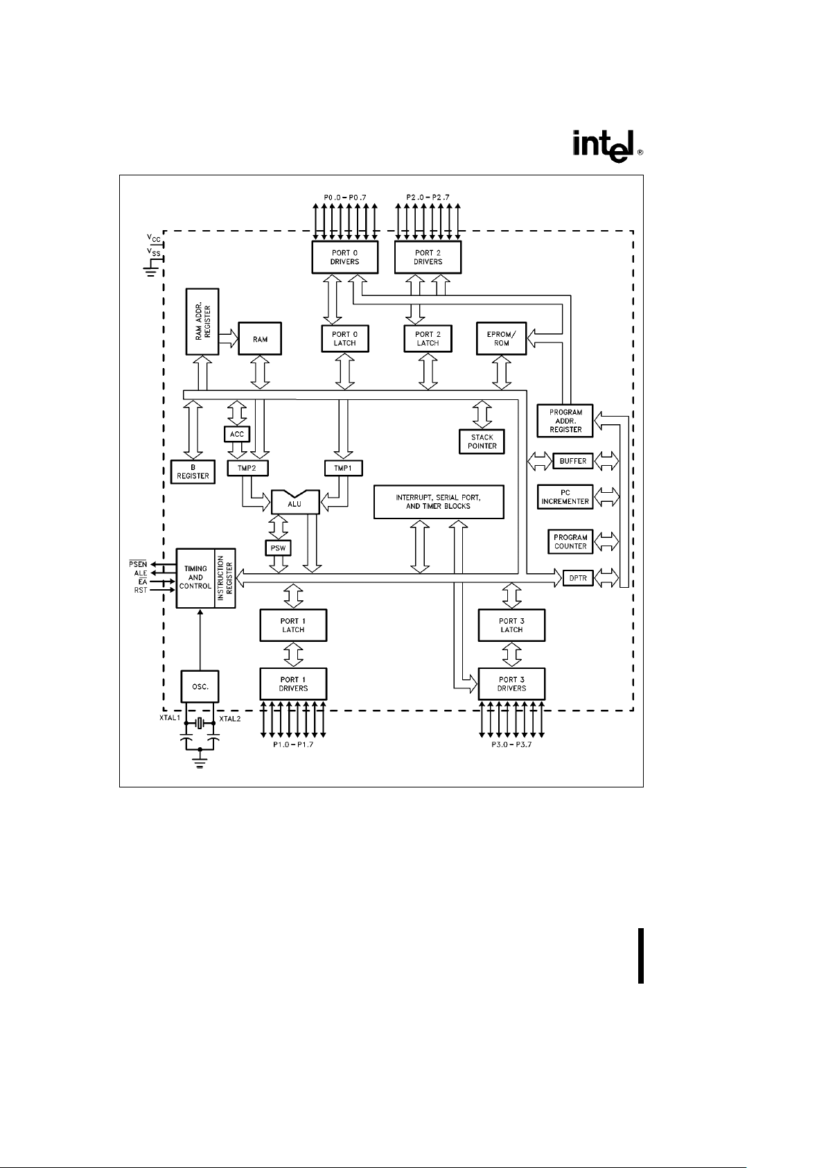
270419– 1
Figure 1. MCSÉ51 Microcontroller Architectural Block Diagram
2
Page 3
AUTOMOTIVE 80C31BH/80C51BH/87C51
80C31BH/80C51BH/87C51
PRODUCT OPTIONS
Intel’s extended and automotive temperature range
products are designed to meet the needs of those
applications whose operating requirements exceed
commercial standards.
With the extended temperature range option, operational characteristics are guaranteed over the temperature range of
b
40§Ctoa85§C ambient. For the
automotive temperature range option, operational
characteristics are guaranteed over the temperature
range of
b
40§Ctoa125§C ambient.
The automotive and extended temperature versions
of the MCS 51 microcontroller product families are
available with or without burn-in options as listed in
Table 1.
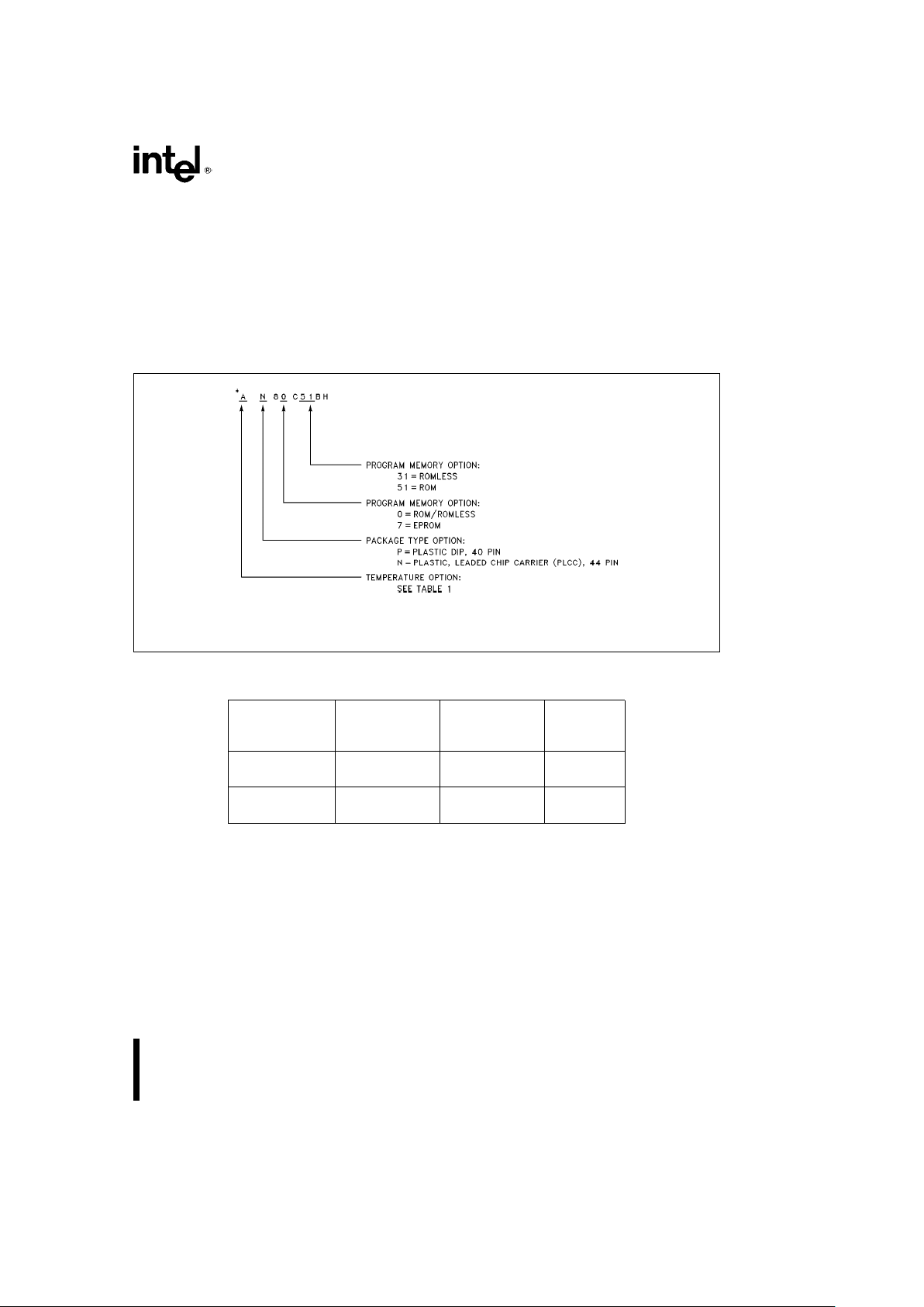
As shown in Figure 2, temperature, burn-in, and
package options are identified by a one- or two-letter
prefix to the part number.
270419– 2
*Example:
AN80C51 indicates an automotive temperature range version of the 80C51 in a PLCC package with 4 Kbyte ROM
program memory.
Figure 2. MCSÉ51 Microcontroller Product Family Nomenclature
Table 1. Temperature Options
Temperature Temperature
Operating
Burn-In
Classification Designation
Temperature
Options
§
C Ambient
Extended T
b
40 toa85 Standard
L
b
40 toa85 Extended
Automotive A
b
40 toa125 Standard
B
b
40 toa125 Extended
3
Page 4
AUTOMOTIVE 80C31BH/80C51BH/87C51
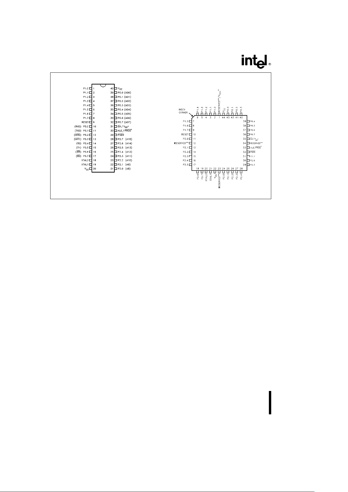
Diagrams are for pin reference only. Package sizes are not to scale.
270419– 3
Pin (PDIP)
*EPROM only
**Do not connect reserved pins
270419– 4
Pad (PLCC)
Figure 3. Pin Connections
PIN DESCRIPTION
VCC: Supply voltage during normal, Idle, and Power
Down operations.
VSS: Circuit ground.
V
SS1
: V
SS1
Ð(EPROM PLCC only) secondary
ground. Provided to reduce ground bounce and improve power supply bypassing.
NOTE:
This pin is not a substitute for the V
SS
pin (pin 22).
For ROM and ROMless, pin 1 is reservedÐdo not
connect.
Port 0: Port 0 is an 8-bit open drain bidirectional I/O
port. As an output port each pin can sink 8 LS TTL
inputs. Port 0 pins that have 1s written to them float,
and in that state can be used as high-impedance
inputs.
Port 0 is also the multiplexed low-order address and
data bus during accesses to external memory. In this
application it uses strong internal pullups when emitting 1s.
Port 0 also receives the code bytes during EPROM
programming, and outputs the code bytes during
program verification. External pullups are required
during program verification.
Port 1: Port 1 is an 8-bit bidirectional I/O port with
internal pullups. Port 1 pins that have 1s written to
them are pulled high by the internal pullups, and in
that state can be used as inputs. As inputs, Port 1
pins that are externally being pulled low will source
current (I
IL
, on the datasheet) because of the inter-
nal pullups.
Port 1 also receives the low-order address bytes
during EPROM programming and program verification.
Port 2: Port 2 is an 8-bit bidirectional I/O port with
internal pullups. Port 2 pins that have 1s written to
them are pulled high by the internal pullups, and in
that state can be used as inputs. As inputs, Port 2
pins that are externally being pulled low will source
current (I
IL
, on the data sheet) because of the inter-
nal pullups.
Port 2 emits the high-order address byte during
fetches from external Program memory and during
accesses to external Data Memory that use 16-bit
address (MOVX
@
DPTR). In this application it uses
strong internal pullups when emitting 1s.
During accesses to external Data Memory that use
8-bit addresses (MOVX
@
Ri), Port 2 emits the con-
tents of the P2 Special Function Register.
Port 2 also receives some control signals and the
high-order address bits during EPROM programming
and program verification.
Port 3: Port 3 is an 8-bit bidirectional I/O port with
internal pullups. Port 3 pins that have 1s written to
them are pulled high by the internal pullups, and in
that state can be used as inputs. As inputs, Port 3
pins that are externally being pulled low will source
current (I
IL
, on the datasheet) because of the pull-
ups.
4
Page 5
AUTOMOTIVE 80C31BH/80C51BH/87C51
Port 3 also serves the functions of various special
features of the MCS 51 microcontroller family, as
listed below:
Pin Name Alternate Function
P3.0 RXD Serial Input Line
P3.1 TXD Serial Output Line
P3.2 INT0 External Interrupt 0
P3.3 INT1
External Interrupt 1
P3.4 T0 Timer 0 External Input
P3.5 T1 Timer 1 External Input
P3.6 WR
External Data Memory Write Strobe
P3.7 RD
External Data Memory Read Strobe
Port 3 also receives some control signals for
EPROM programming and program verification.
RESET: Reset input. A logic high on this pin for two
machine cycles while the oscillator is running resets
the device. An internal pulldown resistor permits a
power-on reset to be generated using only an external capacitor to V
CC
.
ALE/PROG
(EPROM Only): Address Latch Enable
output signal for latching the low byte of the address
during accesses to external memory. This pin is also
the program pulse input (PROG
) during E PROM pro-
gramming.
In normal operation ALE is emitted at a constant
rate of 1/6 the oscillator frequency, and may be
used for external timing or clocking purposes. Note,
however, that one ALE pulse is skipped during each
access to external Data Memory.
PSEN
: Program Store Enable is the Read strobe
to External Program Memory. When the
87C51/80C51BH is executing from Internal Program
Memory, PSEN
is inactive (high). When the device is
executing code from External Program Memory,
PSEN
is activated twice each machine cycle, except
that two PSEN
activations are skipped during each
access to External Data Memory.
EA
/VPP: External Access enable. EA must be
strapped to V
SS
in order to enable the
87C51/80C51BH to fetch code from External Program Memory locations starting at 0000H up to
0FFFFH.[Note, however, that if either of the Lock
Bits is programmed, the logic level at EA is internally
latched during reset.](EPROM only.)
EA
must be strapped to VCCfor internal program
execution.
V
PP
(EPROM Only): This pin also receives the
12.75V programming supply voltage (V
PP
) during
EPROM programming.
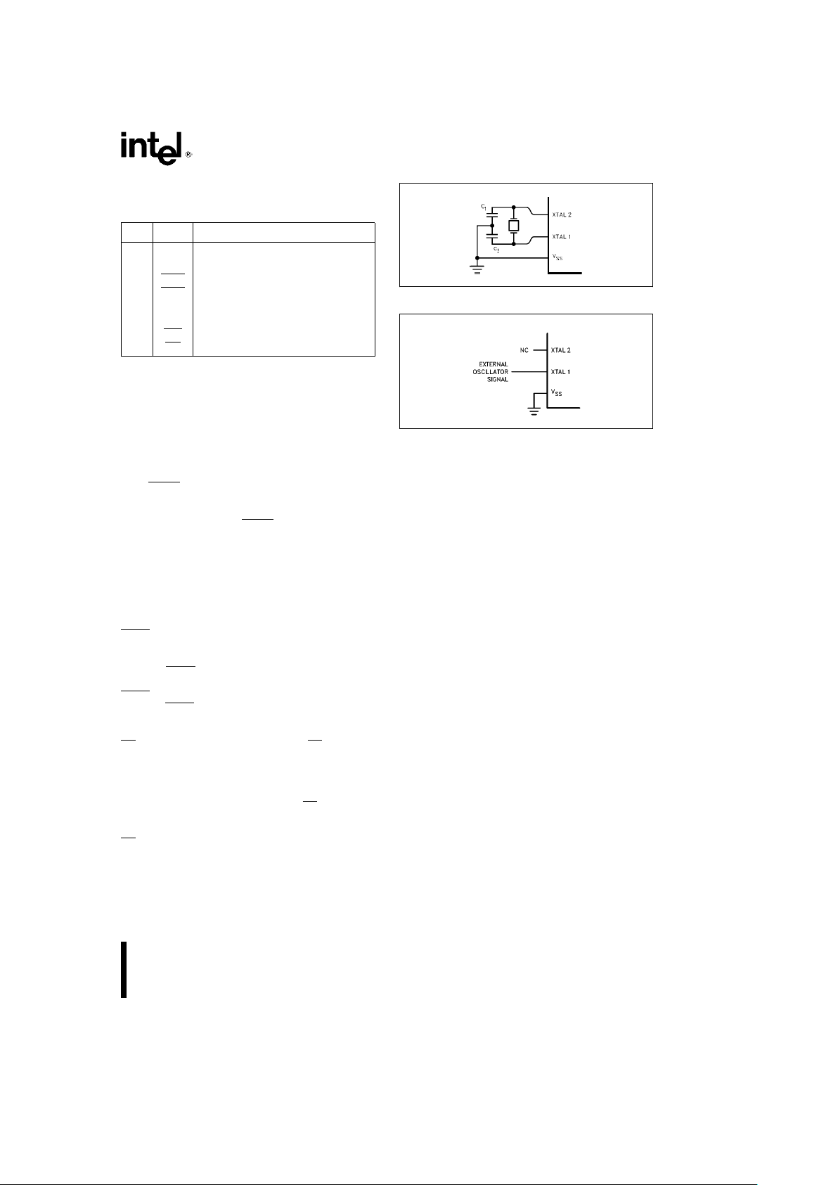
270419– 5
Figure 4. Using the On-Chip Oscillator
270419– 6
Figure 5. External Clock Drive
XTAL1: Input to the inverting oscillator amplifier and
input to the internal clock generating circuits.
XTAL2: Output from the inverting oscillator amplifier.
OSCILLATOR CHARACTERISTICS
XTAL1 and XTAL2 are the input and output, respectively, of an inverting amplifier which can be configured for use as an on-chip oscillator, as shown in
Figure 4.
To drive the device from an external clock source,
XTAL1 should be driven, while XTAL2 is left unconnected, as shown in Figure 5. There are no requirements on the duty cycle of the external clock signal,
since the input to the internal clocking circuitry is
through a divide-by-two flip-flop, but minimum and
maximum high and low times specified on the Datasheet must be observed.
IDLE MODE
In Idle Mode, the CPU puts itself to sleep while all
the on-chip peripherals remain active. The mode is
invoked by software. The content of the on-chip
RAM and all the Special Functions Registers remain
unchanged during this mode. The Idle Mode can be
terminated by any enabled interrupt or by a hardware reset.
It should be noted that when Idle is terminated by a
hardware reset, the device normally resumes program execution, from where it left off, up to two machine cycles before the internal reset algorithm
takes control. On-chip hardware inhibits access to
5
Page 6

AUTOMOTIVE 80C31BH/80C51BH/87C51
Table 2. Status of the External Pins During Idle and Power Down
Mode
Program
ALE PSEN PORT0 PORT1 PORT2 PORT3
Memory
Idle Internal 1 1 Data Data Data Data
Idle External 1 1 Float Data Address Data
Power Down Internal 0 0 Data Data Data Data
Power Down External 0 0 Float Data Data Data
NOTE:
For more detailed information on the reduced power modes refer to current Embedded Applications Handbook, and Application Note AP-252, ‘‘Designing with the 80C51BH.’’
internal RAM in this event, but access to the port
pins is not inhibited. To eliminate the possibility of an
unexpected write to a port pin when Idle is terminated by reset, the instruction following the one that
invokes Idle should not be one that writes to a port
pin or to external memory.
POWER DOWN MODE
In the Power Down mode the oscillator is stopped,
and the instruction that invokes Power Down is the
last instruction executed. The on-chip RAM and
Special Function Registers retain their values until
the Power Down mode is terminated.
The only exit from Power Down is a hardware reset.
Reset redefines the SFRs but does not change the
on-chip RAM. The reset should not be activated before V
CC
is restored to its normal operating level and
must be held active long enough to allow the oscillator to restart and stabilize.
DESIGN CONSIDERATIONS
#
At power on, the voltage on VCCand RST must
come up at the same time for a proper start-up.
#
Before entering the Power Down mode the contents of the Carry Bit and B.7 must be equal.
#
When the Idle mode is terminated by a hardware
reset, the device normally resumes program execution, from where it left off, up to two machine
cycles before the internal reset algorithm takes
control. On-chip hardware inhibits access to internal RAM in this event, but access to the port pins
in not inhibited. To eliminate the possibility of an
unexpected write when Idle is terminated by reset, the instruction following the one that invokes
Idle should not be one that writes to a port pin or
to external memory.
#
An external oscillator may encounter as much as
a 100 pF load at XTAL1 when it starts up. This is
due to interaction between the amplifier and its
feedback capacitance. Once the external signal
meets the VILand VIHspecifications the capacitance will not exceed 20 pF.
#
For EPROM versions exposure to light when the
device is in operation may cause logic errors. For
this reason, it is suggested that an opaque label
be placed over the window when the die is exposed to ambient light.
6
Page 7

AUTOMOTIVE 80C31BH/80C51BH/87C51
PROGRAM MEMORY LOCK
(EPROM Only)
The 87C51 contains two program memory lock
schemes: Encrypted Verify and Lock Bits.
Encrypted Verify: The 87C51 implements a 32byte EPROM array that can be programmed by the
customer, and which can then be used to encrypt
the program code bytes during EPROM verification.
The EPROM verification procedure is performed as
usual, except that each code byte comes out logically X-NORed with one of the 32 key bytes. The key
bytes are gone through in sequence. Therefore, to
read the ROM code, one has to know the 32 key
bytes in their proper sequence.
Lock Bits: Also on the chip are two Lock Bits which
can be left unprogrammed (U) or can be programmed (P) to obtain the following additional features:
Bit 1 Bit 2 Additional Features
U U none
PU
#
Externally fetched code can not
access internal Program Memory.
#
Further programming disabled.
U P (Reserved for Future definition.)
PP
#
Externally fetched code can not
access internal Program Memory.
#
Further programming disabled.
#
Program verification is disabled.
When Lock Bit 1 is programmed, the logic level at
the EA
pin is sampled and latched during reset. If
the device is powered up without a reset, the latch
initializes to a random value, and holds that value
until reset is activated. It is necessary that the
latched value of EA be in agreement with the current
logic level at that pin in order for the device to function properly.
ONCE MODE
The ONCE (‘‘on-circuit emulation’’) mode facilitates
testing and debugging of systems using the 87C51
without the 87C51 having to be removed from the
circuit. The ONCE mode is invoked by:
1. Pull ALE low while the device is in reset and
PSEN
is high;
2. Hold ALE low as RST is deactivated.
While the device is in ONCE mode, the Port 0 pins
go into a float state, and the other port pins and ALE
and PSEN are weakly pulled high. The oscillator circuit remains active. While the 87C51 is in this mode,
an emulator or test CPU can be used to drive the
circuit. Normal operation is restored when a normal
reset is applied.
7
Page 8

AUTOMOTIVE 80C31BH/80C51BH/87C51
ABSOLUTE MAXIMUM RATINGS*
Ambient Temperature Under Biasb40§Ctoa125§C
Storage Temperature ААААААААААb65§Ctoa150§C
Voltage on EA
/VPPPin to VSSААААААА0V toa13.0V
Voltage on Any Other Pin to VSSÀÀb0.5V toa6.5V
IOLper I/O pin ААААААААААААААААААААААААААА15 mA
Power DissipationАААААААААААААААААААААААААА1.5W
(Based on package heat transfer limitations, not device power consumption).
Typical Junction Temperature (T
J
) ААААААААa135§C
(Based upon ambient temperature ata125§C)
Typical Thermal Resistance Junction-to-Ambient
(i
JA
):
PDIP АААААААААААААААААААААААААААААА75
§
C/W
PLCCАААААААААААААААААААААААААААААА46
§
C/W
NOTICE: This is a production data sheet. The specifications are subject to change without notice.
*
WARNING: Stressing the device beyond the ‘‘Absolute
Maximum Ratings’’ may cause permanent damage.
These are stress ratings only. Operation beyond the
‘‘Operating Conditions’’ is not recommended and extended exposure beyond the ‘‘Operating Conditions’’
may affect device reliability.
DC CHARACTERISTICS:
(T
A
eb
40§Ctoa125§C; V
CC
e
5Vg10% (5Vg20% EPROM Only); V
SS
e
0V)
Symbol Parameter Min Typ(1)
Max
Unit
Test
(87C51/80C51BH) Conditions
V
IL
Input Low Voltage (Except EA)
b
0.5 0.2 V
CC
b
0.25 V
V
IL1
Input Low Voltage to EA 0 0.2 V
CC
b
0.45 V
V
IH
Input High Voltage (Except XTAL1, RST) 0.2V
CC
a
1.0 V
CC
a
0.5 V
V
IH1
Input High Voltage (XTAL1, RST) 0.7 V
CC
a
0.1 V
CC
a
0.5 V
V
OL
Output Low Voltage (Ports 1, 2, 3) 0.45
(7)
VI
OL
e
1.6 mA
(2)
V
OL1
Output Low Voltage (Port 0, ALE, PSEN) 0.45
(7)
VI
OL
e
3.2 mA
(2)
V
OH
Output High Voltage 2.4 V I
OH
eb
60 mA
(Ports 1, 2, 3, ALE, PSEN)
0.9 V
CC
VI
OH
eb
10 mA
V
OH1
Output High Voltage (Port 0 in 2.4 V I
OH
eb
800 mA
External Bus Mode)
0.9 V
CC
VI
OH
eb
80 mA
(3)
I
IL
Logical 0 Input Current (Ports 1, 2, 3)
b
75 mAV
IN
e
0.45 V
I
TL
Logical 1-to-0 transition current
b
750 mA
(4)
(Ports 1, 2, 3)
I
LI
Input Leakage Current (Port 0)
g
10 mAV
IN
e
VILor V
IH
I
CC
Power Supply Current:
Active Mode
@
12 MHz
(5)
11.5 25/20 mA
Idle Mode
@
12 MHz
(5)
1.3 6/5 mA
(6)
Power Down Mode 3 100/75 mAV
CC
e
2.2V to 5.5V
RRST Internal Reset Pulldown Resistor 50 300 KX
CIO Pin Capacitance 10 pF
NOTES:
1. ‘‘Typicals’’ are based on a limited number of samples taken from early manufacturing lots and are not guaranteed. The
values listed are at room temp, 5V.
2. Capacitive loading on Ports 0 and 2 may cause spurious noise pulses to be superimposed on the V
OL
s of ALE and Ports
1 and 3. The noise is due to external bus capacitance discharging into the Port 0 and Port 2 pins when these pins make 1to-0 transitions during bus operations. In the worst cases (capacitive loading
l
100pF), the noise pulse on the ALE pin may
exceed 0.8V. In such cases it may be desirable to qualify ALE with a Schmitt Trigger, or use an address latch with a Schmitt
Trigger STROBE input.
3. Capacitive loading on Ports 0 and 2 may cause the V
OH
on ALE and PSEN
to momentarily fall below the 0.9 V
CC
specification when the address bits are stabilizing.
8
Page 9

AUTOMOTIVE 80C31BH/80C51BH/87C51
NOTES: (Continued)
4. Pins of Ports 1, 2 and 3 source a transition current when they are being externally driven from 1 to 0. The transition
current reaches its maximum value when V
IN
is approximately 2V.
5. ICCMAX at other frequencies is given by:
Active Mode: 87C51 ICCMAX
e
0.94cFREQa13.71
80Cx1BH ICCMAX
e
1.47cFREQa2.36
Idle Mode: ICCMAX
e
0.14cFREQa3.81
where FREQ is the external oscillator frequency in MHz. ICCMAX is given in mA. See Figure 6.
6. See Figures 7 through 10 for I
CC
test conditions. Minimum VCCfor Power Down is 2.0V.
7. Under steady state (non-transient) conditions, I
OL
must be externally limited as follows:
Maximum I
OL
per port pin: 10 mA
Maximum I
OL
per 8-bit port
Port 0: 26 mA
Ports 1, 2, and 3: 15 mA
Maximum total I
OL
for all output pins: 71 mA
If I
OL
exceeds the test condition, VOLmay exceed the related specification. Pins are not guaranteed to sink current greater
than the listed test conditions.
270419– 7
Figure 6. ICCvs. FREQ. Valid only
within frequency specifications of the
device under test.
270419– 8
Figure 7. ICCTest Condition, Active Mode.
All other pins are disconnected.
270419– 10
Figure 8. ICCTest Condition, Idle Mode.
All other pins are disconnected.
270419– 11
Figure 9. ICCTest Condition, Power Down
Mode. All other pins are disconnected.
270419– 9
Figure 10. Clock Signal Waveform for ICCtests in Active and Idle Modes.
T
CLCH
e
T
CHCL
e
5 ns.
9
Page 10

AUTOMOTIVE 80C31BH/80C51BH/87C51
EXPLANATION OF THE AC SYMBOLS
Each timing symbol has 5 characters. The first character is always a ‘T’ (stands for time). The other
characters, depending on their positions, stand for
the name of a signal or the logical status of that
signal. The following is a list of all the characters and
what they stand for.
A:Address.
C:Clock.
D:Input data.
H:Logic level HIGH.
I:Instruction (program memory contents).
L:Logic level LOW, or ALE.
P:PSEN
.
Q:Output data.
R:RD
signal.
T:Time.
V:Valid.
W:WR
signal.
X:No longer a valid logic level.
Z:Float.
For example,
T
AVLL
e
Time from Address Valid to ALE Low.
T
LLPL
e
Time from ALE Low to PSEN Low.
AC CHARACTERISTICS: (T
A
eb
40§Ctoa125§C; V
CC
e
5Vg10% (5Vg20% EPROM Only);
V
SS
e
0V; Load Capacitance for Port 0, ALE, and PSENe100 pF; Load Capacitance for All Other
Outputs
e
80 pF)
EXTERNAL PROGRAM AND DATA MEMORY CHARACTERISTICS
Symbol Parameter
12 MHz Osc Variable Oscillator
Units
Min Max Min Max
1/T
CLCL
Oscillator Frequency MHz
87C51/80C51BH/80C31BH 3.5 12–16
T
LHLL
ALE Pulse Width 127 2T
CLCL
b
40 ns
T
AVLL
Address Valid to ALE Low 28 T
CLCL
b
55 ns
T
LLAX
Address Hold After ALE Low 48 T
CLCL
b
35 ns
T
LLIV
ALE Low to Valid Instr In 224 4T
CLCL
b
110 ns
T
LLPL
ALE Low to PSEN Low 43 T
CLCL
b
40 ns
T
PLPH
PSEN Pulse Width 205 3T
CLCL
b
45 ns
T
PLIV
PSEN Low to Valid Instr In 135 3T
CLCL
b
115 ns
T
PXIX
Input Instr Hold After PSEN 00 ns
T
PXIZ
Input Instr Float After PSEN 59 T
CLCL
b
25 ns
T
AVIV
Address Valid to Valid Instr In 312 5T
CLCL
b
105 ns
T
PLAZ
PSEN Low to Address Float 10 10 ns
T
RLRH
RD
Pulse Width 400 6T
CLCL
b
100 ns
T
WLWH
WR Pulse Width 400 6T
CLCL
b
100 ns
T
RLDV
RD Low to Valid Data In 252 5T
CLCL
b
165 ns
T
RHDX
Data Hold After RD High 0 0 ns
T
RHDZ
Data Float After RD High 97 2T
CLCL
b
70 ns
T
LLDV
ALE Low to Valid Data In 517 8T
CLCL
b
150 ns
T
AVDV
Address Valid to Valid Data In 585 9T
CLCL
b
165 ns
T
LLWL
ALE Low to RD or WR Low 200 300 3T
CLCL
b
50 3T
CLCL
a
50 ns
T
AVWL
Address Valid to RD or WR Low 203 4T
CLCL
b
130 ns
T
QVWX
Data Valid to WR Transition 23 T
CLCL
b
60 ns
T
WHQX
Data Hold After WR High 33 T
CLCL
b
50 ns
T
RLAZ
RD Low to Address Float 0 0 ns
T
WHLH
RD or WR High to ALE High 43 123 T
CLCL
b
40 T
CLCL
a
40 ns
10
Page 11

AUTOMOTIVE 80C31BH/80C51BH/87C51
EXTERNAL PROGRAM MEMORY READ CYCLE
270419– 12
EXTERNAL DATA MEMORY READ CYCLE
270419– 13
EXTERNAL DATA MEMORY WRITE CYCLE
270419– 14
11
Page 12

AUTOMOTIVE 80C31BH/80C51BH/87C51
EXTERNAL CLOCK DRIVE
Symbol Parameter Min Max Units
1/T
CLCL
Oscillator Frequency 3.5 12 MHz
3.5 16
T
CHCX
High Time 20 ns
T
CLCX
Low Time 20 ns
T
CLCH
Rise Time 20 ns
T
CHCL
Fall Time 20 ns
EXTERNAL CLOCK DRIVE WAVEFORM
270419– 17
SERIAL PORT TIMINGÐSHIFT REGISTER MODE
12 MHz Variable
Symbol Parameter Oscillator Oscillator Units
Min Max Min Max
T
XLXL
Serial Port Clock Cycle Time 1.0 12T
CLCL
ms
T
QVXH
Output Data Setup to Clock Rising Edge 700 10T
CLCL
b
133 ns
T
XHQX
Output Data Hold After Clock Rising Edge 50 2T
CLCL
b
117 ns
T
XHDX
Input Data Hold After Clock Rising Edge 0 0 ns
T
XHDV
Clock Rising Edge to Input Data Valid 700 10T
CLCL
b
133 ns
SHIFT REGISTER MODE TIMING WAVEFORMS
270419– 15
AC TESTING INPUT, OUTPUT WAVEFORMS
270419– 16
AC inputs during testing are driven at V
CC
b
0.5 for a Logic ‘‘1’’
and 0.45V for a Logic ‘‘0.’’ Timing measurements are made at V
IH
min for a Logic ‘‘1’’ and VILmax for a Logic ‘‘0’’.
FLOAT WAVEFORMS
270419– 18
For timing purposes a port pin is no longer floating when a 100
mV change from load voltage occurs, and begins to float when a
100 mV change from the loaded VOH/VOLlevel occurs. IOL/I
OH
t
g
20 mA.
12
Page 13

AUTOMOTIVE 80C31BH/80C51BH/87C51
EPROM CHARACTERISTICS
(EPROM Only)
The 87C51 is programmed by a modified QuickPulse Programming algorithm. It differs from older
methods in the value used for V
PP
(Programming
Supply Voltage) and in the width and number of the
ALE/PROG
pulses.
The 87C51 contains two signature bytes that can be
read and used by an EPROM programming system
to identify the device. The signature bytes identify
the device as an 87C51 manufactured by Intel.
Table 3 shows the logic levels for reading the signature byte, and for programming the Program Memory, the Encryption Table, and the Lock Bits. The circuit configuration and waveforms for Quick-Pulse
Programming are shown in Figures 11 and 12. Figure 13 shows the circuit configuration for normal
Program Memory verification.
Table 3. EPROM Programming Modes
MODE RST PSEN
ALE/ EA/
P2.7 P2.6 P3.7 P3.6
PROG
V
PP
Read Signature 1 0 1 1 0 0 0 0
Program Code Data 1 0 0* V
PP
1011
Verify Code Data 1 0 1 1 0 0 1 1
Pgm Encryption Table 1 0 0* V
PP
1010
Pgm Lock Bit 1 1 0 0* V
PP
1111
Pgm Lock Bit 2 1 0 0* V
PP
1100
NOTES:
‘‘1’’
e
Valid high for that pin
‘‘0’’
e
Valid low for that pin
V
PP
e
12.75Vg0.25V
V
CC
e
5Vg20% during programming and verification
*ALE/PROG
receives 25 programming pulses while VPPis held at 12.75V. Each programming pulse is low for 100 ms
(
g
10 ms) and high for a minimum of 10 ms.
270419– 19
Figure 11. Programming Configuration
13
Page 14

AUTOMOTIVE 80C31BH/80C51BH/87C51
270419– 20
Figure 12. PROG Waveforms
Quick-Pulse Programming
(EPROM Only)
The setup for Microcontroller Quick-Pulse Programming is shown in Figure 11. Note that the 87C51 is
running with a 4 to 6 MHz oscillator. The reason the
oscillator needs to be running is that the device is
executing internal address and program data transfers.
The address of the EPROM location to be programmed is applied to Ports 1 and 2, as shown in
Figure 11. The code byte to be programmed into
that location is applied to Port 0. RST, PSEN
, and
pins of Ports 2 and 3 specified in Table 3 are held at
the ‘‘Program Code Data’’ levels indicated in Table
2. Then ALE/PROG
is pulsed low 25 times as
shown in Figure 12.
To program the Encryption Table, repeat the 25pulse programming sequence for addresses 0
through 1FH, using the ‘‘Pgm Encryption Table’’ levels. Don’t forget that after the Encryption Table is
programmed, verify cycles will produce only encrypted data.
To program the Lock Bits, repeat the 25-pulse programming sequence using the ‘‘Pgm Lock Bit’’ levels. After one Lock Bit is programmed, further programming of the Code Memory and Encryption Table is disabled. However, the other Lock Bit can still
be programmed.
Note that the EA
/VPPpin must not be allowed to go
above the maximum specified V
PP
level for any
amount of time. Even a narrow glitch above that voltage level can cause permanent damage to the device. The V
PP
source should be well regulated and
free of glitches and overshoot.
270419– 21
Figure 13. Program Verification
14
Page 15

AUTOMOTIVE 80C31BH/80C51BH/87C51
Program Verification
(EPROM Only)
If Lock Bit 2 has not been programmed, the on-chip
Program Memory can be read out for program verification. The address of the Program Memory location
to be read is applied to Ports 1 and 2 as shown in
Figure 13. The other pins are held at the ‘‘Verify
Code Data’’ levels indicated in Table 3. The contents of the addressed location will be emitted on
Port 0. External pullups are required on Port 0 for
this operation. Detailed timing specifications are
shown in later sections of this datasheet.
If the Encryption Table has been programmed, the
data presented at Port 0 will be the Exclusive NOR
of the program byte with one of the encryption bytes.
The user will have to know the Encryption Table
contents in order to correctly decode the verification
data. The Encryption Table itself can not be read
out.
Reading the Signature Bytes
(EPROM Only)
The signature bytes are read by the same procedure
as a normal verification of locations 030H and 031H,
except that P3.6 and P3.7 need to be pulled to a
logic low. The values returned are:
(030H)
e
89H indicates manufactured by Intel
(031H)e57H indicates 87C51
Program/Verify Algorithms
(EPROM Only)
Any algorithm in agreement with the conditions listed in Table 3, and which satisfies the timing specifications, is suitable.
Erasure Characteristics
(EPROM Only)
Erasure of the EPROM begins to occur when the
chip is exposed to light with wavelengths shorter
than approximately 4,000 Angstroms. Since sunlight
and fluorescent lighting have wavelengths in this
range, exposure to these light sources over an extended time (about 1 week in sunlight, or 3 years in
room level fluorescent lighting) could cause inadvertent erasure. If an application subjects the device to
this type of exposure, it is suggested that an opaque
label be placed over the window.
The recommended erasure procedure is exposure
to ultraviolet light (at 2537 Angstroms) to an integrated dose of at least 15 W-sec/cm
2
. Exposing the
EPROM to an ultraviolet lamp of 12,000 mW/cm
2
rating for 30 minutes, at a distance of about 1 inch,
should be sufficient.
Erasure leaves the array in an all 1s state.
EPROM PROGRAMMING AND VERIFICATION CHARACTERISTICS:
(T
A
e
21§Cto27§C, V
CC
e
5Vg20%, V
SS
e
0V)
Symbol Parameter Min Max Units
V
PP
Programming Supply Voltage 12.5 13.0 V
I
PP
Programming Supply Current 50 mA
1/T
CLCL
Oscillator Frequency 4 6 MHz
T
AVGL
Address Setup to PROG Low 48T
CLCL
T
GHAX
Address Hold After PROG 48T
CLCL
T
DVGL
Data Setup to PROG Low 48T
CLCL
T
GHDX
Data Hold After PROG 48T
CLCL
T
EHSH
P2.7 (ENABLE) High to V
PP
48T
CLCL
T
SHGL
VPPSetup to PROG Low 10 ms
T
GHSL
VPPHold After PROG 10 ms
T
GLGH
PROG Width 90 110 ms
T
AVQV
Address to Data Valid 48T
CLCL
T
ELQV
ENABLE Low to Data Valid 48T
CLCL
T
EHQZ
Data Float After ENABLE 0 48T
CLCL
T
GHGL
PROG High to PROG Low 10 ms
15
Page 16

AUTOMOTIVE 80C31BH/80C51BH/87C51
EPROM PROGRAMMING AND VERIFICATION WAVEFORMS
270419– 22
*FOR PROGRAMMING CONDITIONS SEE FIGURE 11.
FOR VERIFICATION CONDITIONS SEE FIGURE 13.
DATASHEET REVISION SUMMARY
The following are the key differences between this datasheet and the -006 version:
1. The ‘‘preliminary’’ status was removed and replaced with production status (no label).
2. Trademark was updated.
The following are the key differences between the -005 and the -006 version of the datasheet:
1. Preliminary notice added to Title page.
2. Figure 3 Pin Connections the NC** pins are now Reserved** pins.
3. Figure 3 Pin Connections RST pin is now RESET pin.
4. RST pin description is now RESET pin description.
5. Figure 4 the capacitor values have been removed.
6. CERDIP part reference in the D.C. Characteristics section has been removed.
7. I
CC
Max characteristics have been corrected to reflect test program conditions.
8. T
AVIV
and T
RLDV
formulas changed to correlate 12 MHz timings.
The following are the key differences between the -004 and the -005 version of this datasheet:
1. Removed references to burn-in options in Table 1 and added explanation of burn-in offered. Removed
references to commercial temperatures.
2. Deleted reference to ‘‘
b
1’’ designation 16 MHz.
3. Differentiated VCCfor ROM/ROMless and EPROM.
The following are the key differences between the -002 and the -003 version of this datasheet:
1. Changed the title to 80C31BH/80C51BH/87C51 CHMOS Single-Chip 8-Bit Microcontroller.
2. Added the pin count for each package version in Figure 2.
3. Removed references to burn-in options in Table 1.
4. Added external oscillator start-up design considerations.
The following are the key differences between the -002 and the -001 version of the 80C51BH datasheet:
1. Maximum I
OL
per I/O pin added.
2. Note 7 on Maximum Current Specifications added to DC Characterstics.
3. Datasheet Revision Summary added.
16
 Loading...