

Datasheet TN815-800B, TN815-700B, TN815-600B, TN815-400B, TN805-800B Datasheet (SGS Thomson Microelectronics)
...Page 1
®
FEATURES
I
= 8 A
TRMS
V
= 400 V t o 800 V
DRM
IGT ≤ 5 mA and 15 mA
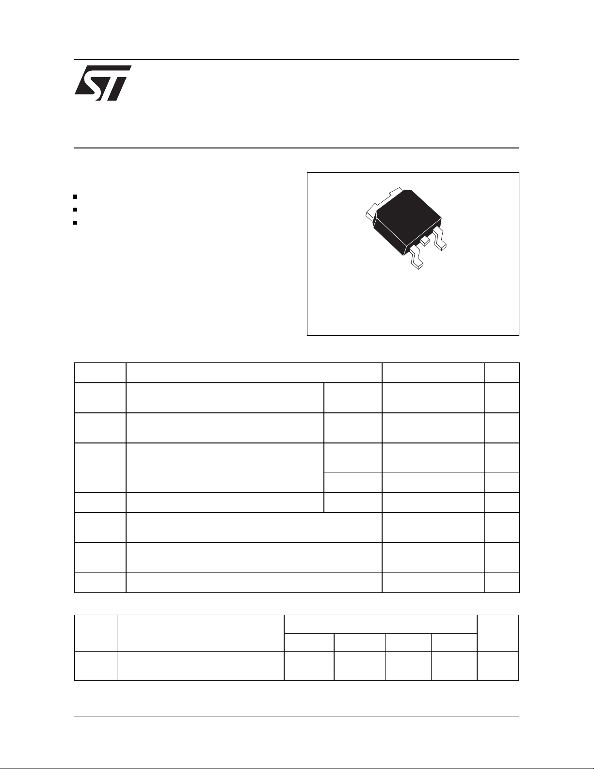
TN805/TN815-B
SCR’s
A
DESCRIPTION
G
A
The TN805/TN815-B serie of Silicon Controlled
Rectifiers uses a high performance TOPGLASS
K
PNPN technology.
These parts are intended for general purpose
applications using mount technology.
DPAK
ABSOLUTE MAXIMUM RATINGS
Symbol Parameter Value Unit
I
T(RMS)
RMS on-state current
Tc= 105°C8 A
(180° conduction angle)
I
T(AV)
Mean on-state current
Tc= 105°C5 A
(180° conduction angle)
I
TSM
Non repetitive surge peak on-state current
tp = 8.3 ms 73 A
(Tj initial = 25°C)
tp = 10 ms 70
2
I
tI
dI/dt Critical rate of rise of on-state current
2
t Value for fusing tp = 10ms 24.5 A2s
100 A/µs
= 100 mA dIG /dt = 1 A/µs.
I
G
T
stg
T
j
Storage junction temperature range
Operating junction temperature range
Tl Maximum lead temperature for s oldering during 10s 260
TN805 or TN815
Symbol Parameter
400B 600B 700B 800B
V
DRM
V
RRM
August 1998 - Ed: 1A
Repetitive peak-off voltage
Tj = 125°C
400 600 700 800 V
- 40 to + 150
- 40 to + 125
°
°
Unit
C
C
1/5
Page 2
TN805/TN815-B
THERMAL RESISTANCES
Symbol Parameter Value Unit
2
Rth(j-a) Junction to ambient (S=0.5cm
)70
°
C/W
Rth(j-c) Junction to case for D .C 2.5
GATE CHARACTERISTICS
P
= 1W PGM = 10 W (tp = 20 µs) IGM = 4 A (tp = 20 µs) V
G (AV)
= 5 V
RGM
ELECTRICAL CHARACTERISTICS
Symbol Test Conditions Type
TN805 TN815
TM
Ω
Ω
= 3 x I
T(AV)
Tj= 25°CMAX 5 15
Tj= 25°C MAX 1.5 V
Tj= 25°C TY P 2
I
GT
V
GT
V
GD
tgt V
VD = 12V (DC) RL= 33
VD = 12V (DC) RL= 33
VD = V
= V
D
RL = 3.3kΩ Tj= 125°CMIN 0.2 V
DRM
I
DRM
IG = 40mA dIG/dt = 0.5A/us
I
H
IT= 150mA Gate open Tj= 25°C MAX 25 30 mA
Value
°
C/W
Unit
µ
µ
A
s
I
L
V
TM
I
DRM
I
RRM
IG = 1.2 I
GT
ITM= 16A tp= 380µs
VDRM Rated
VRRM Rated Tj = 125°C MAX 2 mA
dV/dt Linear slope up to
=67%V
V
D
DRM
ORDERING INFORMATION
SCR
CURRENT
Tj= 25°C MAX 25 30 mA
Tj= 25°CMAX 1.6 V
Tj= 25°CMAX 10
Tj= 125°CMIN 50 150 V/
Gate open
TN 8 05 - 600 B
SENSITIVITY
PACKAG ES :
B: DPA K
/ V
V
DRM
RRM
µ
A
µ
s
2/5
Page 3

TN805/815-B
Fig. 1:
Maximum average power dissipation ver-
sus average on-state current .
P(W)
8
7
6
5
α = 30°
α = 60°
α = 90°
α = 120°
α = 180°
D.C.
4
3
2
1
0
01234567
Fig. 3-1:
Average and D.C. on-state current versus
IT(av)(A)
360°
α
case temperature.
IT(av)(A)
10
D.C.
8
6
4
2
0
0 102030405060708090100110120130
α = 180°
Tcase(°C)
Fig. 2 :
Correlati on b etween maximu m average
power dissipation and maximum allowable temperatures ( T
amb
and T
) for different thermal
case
resistances he atsink+contact.
P(W) Tcase (°C)
8
α = 180°
7
6
5
4
3
2
1
0
Fig. 3-2:
Rth=37°C/W
Tamb(°C)
0 102030405060708090100110120130
Average and D.C. on-state current versus
Rth=0°C/W
105
110
115
120
125
case temperature.
IT(av)(A)
2.0
1.8
1.6
1.4
1.2
1.0
0.8
0.6
0.4
0.2
0.0
0 102030405060708090100110120130
D.C.
α = 180°
Tamb(°C)
Fig. 4-1:
Relative variation of ther mal impedance
versus pulse duration.
K=[Zth(j-c)/Rth(j-c)]
1.0
0.5
0.2
0.1
1E-3 1E-2 1E-1 1E+0
tp(s)
Fig. 4-2:
Relative variation of thermal impedance
versus pulse duration.
K=[Zth(j-a)/Rth(j-a)]
1.00
0.10
0.01
1E-2 1E-1 1E+0 1E+1 1E+2 5E+2
tp(s)
3/5
Page 4

TN805/TN815-B
Fig. 5:
Relative variation of gate trigger current and
holding current versus junction temperature.
Igt,IH[Tj]/Ig,IH[Tj=25°C]
2.0
1.8
1.6
1.4
1.2
1.0
0.8
0.6
0.4
0.2
0.0
-40-200 20406080100120
Fig. 7:
Igt
IH
Tj(°C)
Non repetitive surge peak on-state current
for a sinusoidal pulse with width tp<10ms, and corresponding value of I2t.
ITSM(A),I²t(A²s)
300
ITSM
100
Tj initial=25°C
Fig. 6:
Non repetitive surge peak on-stat e current
versus number of cycles.
ITSM(A)
80
70
60
50
40
30
20
10
0
1 10 100 1000
Fig. 8:
On-state charact eristics (maxi mum va lues).
Number of cycles
ITM(A)
100.0
10.0
Tj=Tj max.
Tj initial=25°C
F=50Hz
Tj max.:
Vto=0.85V
Rt=46m
50
I²t
20
10
12 510
Fig. 9:
Thermal resistance junction to ambient ver-
tp(ms)
sus copper surface under tab (Epoxy printed circuit
board FR4, copper thickness: 35µm).
Rth(j-a) (°C/W)
100
80
60
40
20
0
0 2 4 6 8 10 12 14 16 18 20
S(Cu) (cm²)
1.0
0.1
0.0 0.5 1.0 1.5 2.0 2.5 3.0 3.5 4.0 4.5 5.0
Tj=25°C
VTM(V)
4/5
Page 5

PACKAGE MECHANICAL DATA
DPAK
TN805/815-B
DIMENSIONS
REF.
A 2.20 2.40 0.086 0.094
A1 0.90 1.10 0.035 0.043
A2 0.03 0.23 0.001 0.009
B 0.64 0.90 0.025 0.035
B2 5.20 5.40 0.204 0.212
C 0.45 0.60 0.017 0.023
C2 0.48 0. 60 0.018 0.023
D 6.00 6.20 0.236 0.244
E 6.40 6.60 0.251 0.259
G 4.40 4.60 0.173 0.181
H 9.35 10.10 0.368 0.397
L2 0.80 0.031
L4 0. 60 1.00 0.023 0.039
V2 0° 8° 0° 8°
Millimeters Inches
Min. Typ. Max Min. Typ. Max.
FOOT PRINT DIMENSIONS
6.7
(in millimeters)
WEIGHT :
MARKING
0.30g
TYPE MARKING
6.7
T805- x00B
TN8
05x0
6.7
3
1.61.6
2.32.3
Information furnished is believed to be accurate and reliable. However, STMicroelectronics assumes no responsIbility for the consequences of
use of such information nor for any infringement of patents or other rights of third parties which may result from its use. No license is granted by
implication o r o therwise under an y patent or paten t ri ghts of S TMicroel ectroni cs. Spec ifications mentione d in t his p ublicatio n are subject to
change without notice. This publication supersedes and replaces all information previously supplied.
STMicroelectr oni cs products are not authorized for use as criti cal components in life support devices or systems without express w ritten approval of STMicroelectronics.
The ST logo is a registered trademark of STMicroelectronics
© 1998 STMicroelectronics - Printed in Italy - All rights reserved.
STMicroelectronics GROUP OF COMPANIES
Australia - Brazil - Canada - China - France - Germany - Italy - Japan - Korea - Malaysia - Malta - Mexico - Morocco -
The Netherlands Singapore - Spain - Sweden - Switzerland - Taiwan - Thailand - United Kingdom - U.S.A.
T815-x00B
TN8
15x0
5/5
 Loading...