

Page 1
®
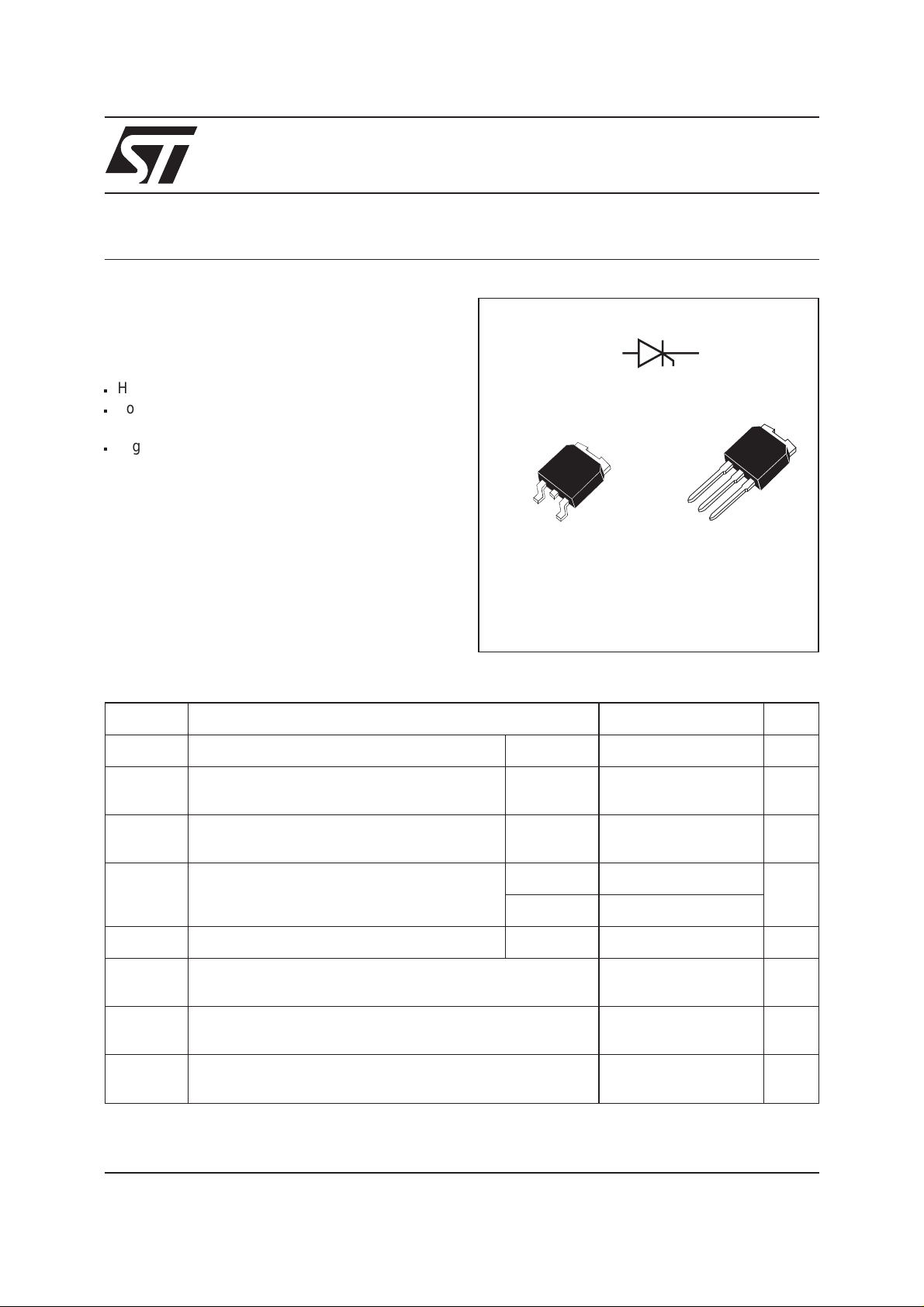
Application Specific Discretes
A.S.D.™
TN22
STARTLIGHT
FEATURES
High clamping voltage structure (1200 - 1500V)
n
Low gate triggering current for direct drive from
n
2, TAB
1
3
line (< 1.5mA)
High holding current (> 175mA), ensuring high
n
TAB
striking energy.
DESCRIPTION
The TN22 has been specifically developed for use
1
2
3
1
2
3
in electronic starter circuits. Use in conjunction
with a sensitive SCR and a resistor, it provides
high energy striking characteristics with low trig-
DPAK
(TN22-B)
IPAK
(TN22-H)
geringpower.Thankstoitselectronicconcept, this
TN22based starter offers high reliabilitylevels and
extended life time of the fluorescent tubelamps.
ABSOLUTE RATINGS (limiting values)
Symbol Parameter Value Unit
V
DRM
I
T(RMS)
Repetitive peak off-state voltage
RMS on-state current
= 110°C 400 V
T
j
Tc= 95°C 2 A
Full sine ware (180° conduction angle)
TAB
I
T(AV)
Mean on-state current
Full sine ware (180° conduction angle)
I
TSM
Non repetitive surge peak on-state current
(T
2
t
I
dI/dt
2
I
t Value for fusing
Critical rate of rise of on-state current
IG=5mA dIG/dt = 70 mA/µs.
T
stg
T
j
Tl
Storage and operating junction temperature range
Maximum lead temperature for soldering during 10s at
4.5mm from case
October 2000 - Ed:1
initial = 25°C)
j
Tc= 95°C 1.8 A
tp = 8.3ms 22 A
tp = 10ms 20
tp = 10ms 2 A
50 A/µs
-40to+150
°C
-40to+110
260 °C
2
s
1/7
Page 2
TN22
THERMAL RESISTANCES
Symbol Parameters Value Unit
Rth(j-a)
Rth(j-c)
Junction to ambient
Junction to case
100 °C/W
3 °C/W
GATE CHARACTERISTICS (maximum values)
P
= 300 mW PGM=2W(tp=20µs) I
G (AV)
=1A(tp=20µs) V
FGM
RGM
=6V
ELECTRICAL CHARACTERISTICS
Symbol Test conditions Type Value Unit
I
GT
V
GT
I
H
V
TM
I
DRM
dV/dt
VD=12V (DC) RL=33Ω
VD=12V (DC) RL=33Ω
=1KΩ
R
GK
VGK=0V
ITM= 2A tp= 380µs
V
Rated
DRM
Linear slope up to
=67%V
V
D
DRMVGK
=0V
Tj= 25°C MAX 1.5 mA
Tj= 25°C MAX 3 V
Tj= 25°C MIN 175 mA
Tj= 25°C MAX 3.1 V
Tj= 25°C MAX 0.1 mA
Tj= 110°C MIN 500 V/µs
Symbol Test conditions Type
V
BR
ID= 5mA VGK= 0V Tj = 25°C
MIN 1200 V
MAX 1500 V
Value
TN22-1500
Unit
2/7
Page 3
TN22
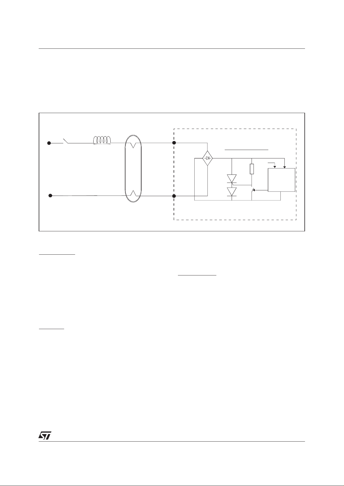
This thyristor has been designed for use as a fluorescent tube starter switch.
An electronic starter circuit provides :
BASIC APPLICATION DIAGRAM
INDUCTANCE
BALLAST
AC
VOLT AGE
FLUORESCENT
TUBE
A pre-heating period during which a heating
■
current is applied to the cathode heaters.
One or several high voltage striking pulses
■
across the lamp.
STARTER CIRCUIT
R
TN22
S
CONTROLLER
(TIMER)
PRINCIPLE OF OPERATION
1/ Pre-heating
At rest the switch S is opened and when the mains
voltage is applied across the circuit a full wave rectified current flows through the resistor R and the
TN22 gate : at every half-cycle when this current
reaches the gate triggering current (I
) the thyris-
GT
tor turns on.
When the device is turned on the heating current,
limited by the ballast choke, flows through the tube
heaters.
The pre-heating time is typically 2 or 3 seconds.
2/ Pulsing
At the end of the pre-heating phase the switch S is
turned on. At this moment :
Ifthe current through the devices is higher than the
holding current (I
the current falls below I
) the thyristor remains on until
H
. Then the thyristor turns
H
off.
If the current is equal or lower than the holding current the thyristor turns off instantaneously.
When the thyristor turns off the current flowing
through the ballast choke generates a high voltage
pulse. This overvoltage is clamped by the thyristor
avalanche characteristic (V
BR
).
Ifthe lamp isnot struck afterthe first pulse,the system starts a new ignition sequence again.
3/ Steady state
When the lamp is on the running voltage is about
150V and the starter switch is in the off-state.
IMPLEMENTATION
The resistor R must be chosen to ensure a proper
triggering in the worst case (minimum operating
temperature) according to the specified gate triggering current and the peak line voltage.
Switch S : This function can be realized with a gate
sensitive SCR type : P0130AA 1EA3
This component is a low voltage device (< 50V)
and the maximum current sunk through this switch
can reach the level of the thyristor holding current.
The pre-heating period can be determined by the
time constant of a capacitor-resistor circuit
charged by the voltage drop of diodes used in series in the thyristor cathode.
3/7
Page 4

TN22
Fig.1 : Maximum average power dissipation ver-
sus average on-state current (rectified full sine
wave).
P(W)
T(av)
6
5
4
3
2
1
0
0
=30
0.2
=60
o
0.4
=120
o
=90
o
0.6 0.8
o
= 180
o
I(A)
T(av)
1.2 1.4 1.6 1.8
1
2
Fig.3 : Average on-state current versus case temperature (rectified full sine wave).
I(A)
T(av)
2.0
1.8
1.6
1.4
1.2
1.0
0.8
0.6
0.4
0.2
0.0
0.0
o
=180
o
Tcase ( C)
10 20 30 40 5 0 60
70
80 90
100 110
Fig.2 : Correlation between maximum average
power dissipation and maximum allowable temperature (Tamb and Tcase) for different thermal
resistances heatsink + contact.
P(W)
T(av)
6
5
o
Rth=12 C/W
o
Rth=8 C/W
o
Rth=4 C/W
o
Rth=0 C/W
4
3
2
=180
o
1
o
0
0
10 20 30 40 50 60 70 80 90 100 110
Tcase ( C)
Fig.4 : Thermal transient impedance junction to
ambient versus pulse duration.
1.0E+02
1.0E+01
1.0E+00
Zth(j-a)(oC/W)
1.0E-01
1.0E-02 1.0E-01
tp(S)
1.0E +00 1.0E +01 1.0E + 02 1.0E +03
Fig.5 : Relative variation of gate trigger current
and holding current versus junction temperature.
Igt[Tj]
Igt[Tj=25 C]
3.0
2.5
2.0
1.5
Ih
1.0
0.5
0.0
-40 -20 0 20 40 60 80 100 120 140
4/7
o
Igt
Ih[Tj]
Ih[Tj=25 C]
o
Tj( C)
o
Fig.6 : Non repetitive surge peak on-state current
versus number of cycles.
I(A)
TSM
20
18
16
14
12
10
8
6
4
2
Number of cycles
0
1 10 100 1000
Tj initial = 25 C
F=50Hz
o
Page 5

TN22
Fig.7 : Non repetitive surge peak on-state current
for a sinusoidal pulse with width : tp = 10ms, and
corresponding value of I
I(A).I2t(A2s)
TSM
00
10
1
1
tp(ms)
2
t.
o
10
I
TSM
I2t
Tj initial = 25 C
Fig.9 : Relative variation of holding current versus
gate-cathode resistance (typical values).
Fig.8 : On-state characteristics (maximum values).
V(V)
TM
8
7
6
5
4
3
2
1
0
0.1
Tj=110 C
Vto =2.50V
Rt =0.235
o
o
Tj=110 C
o
Tj=25 C
I(A)
TM
110
20
Fig.10 : Maximum allowable RMS current versus
time conduction and initial case temperature.
Note : Calculation made fot Tj max = 135°C (the
failure mode will be short circuit)
I(mA)
H
500
100
10
1
1 10 100 1000
Rgk( )
Tj=25 C
ORDERING INFORMATION
TN 2 2 - 1500 B (-TR)
STARTLIGHT
DEVICE
I MAX
T(RMS)
2: 2 A
I MAX
GT
2: 1.5 mA
o
V max:
BR
11
10
9
8
7
6
5
4
3
2
1
1500: 1500V
I(A)
T(rms)
Tc in itial = 25 C
Tc in itial = 65 C
0.1
o
Tc initial = 45 C
o
tp(s)
1 10 100
o
PACKAGE:
B: DPAK
H: IPAK
PACKING MODE:
Blank:Tube
-TR: DPAKTape & Reel
5/7
Page 6

TN22
PACKAGE MECHANICAL DATA
DPAK
DIMENSIONS
REF.
Millimeters Inches
Min. Max Min. Max.
A 2.2 2.4 0.086 0.094
A1 0.9 1.1 0.035 0.043
A2 0.03 0.23 0.001 0.009
B 0.64 0.9 0.025 0.035
B2 5.2 5.4 0.204 0.212
C 0.45 0.6 0.017 0.023
C2 0.48 0.6 0.018 0.023
D 6.0 6.2 0.236 0.244
E 6.4 6.6 0.251 0.259
G 4.4 4.6 0.173 0.181
H 9.35 10.1 0.368 0.397
L2 0.80 typ. 0.031 typ.
L4 0.6 1.0 0.023 0.039
V2 0° 8° 0° 8°
FOOTPRINT
6.7
6.7
3
3
1.61.6
2.32.3
6/7
Page 7

PACKAGE MECHANICAL DATA
IPAK
E
B2
H
L1
L
B6
G
L2
B3
B
V1
B5
TN22
DIMENSIONS
REF.
A
C2
A 2.2 2.4 0.086 0.094
A1 0.9 1.1 0.035 0.043
A3 0.7 1.3 0.027 0.051
B 0.64 0.9 0.025 0.035
B2 5.2 5.4 0.204 0.212
B3 0.85 0.033
D
B5 0.3 0.035
B6 0.95 0.037
C 0.45 0.6 0.017 0.023
C2 0.48 0.6 0.019 0.023
A1
D 6 6.2 0.236 0.244
E 6.4 6.6 0.252 0.260
G 4.4 4.6 0.173 0.181
H 15.9 16.3 0.626 0.641
C
A3
L 9 9.4 0.354 0.370
L1 0.8 1.2 0.031 0.047
L2 0.8 1 0.031 0.039
V1 10° 10°
Millimeters Inches
Min. Typ. Max. Min. Typ. Max.
OTHER INFORMATION
Type Marking Package Weight Base Qty Delivery mode
TN22-1500B
TN22-1500B-TR
TN22-1500H
Informationfurnishedisbelievedtobeaccurateandreliable.However,STMicroelectronicsassumesnoresponsibilityfortheconsequencesof
useofsuchinformation nor for any infringement of patents or other rights of third parties which may result from its use. No license is granted by
implication or otherwise under any patent or patent rights of STMicroelectronics. Specifications mentioned in this publication are subject to
change without notice. This publication supersedes and replaces all information previously supplied.
STMicroelectronics products are not authorized for use as critical components in life support devices or systems without express written approval of STMicroelectronics.
Australia - Brazil - China - Finland - France - Germany - Hong Kong - India - Italy - Japan - Malaysia
Malta - Morocco - Singapore - Spain - Sweden - Switzerland - United Kingdom - U.S.A.
TN221500 DPAK 0.3g 75 Tube
TN221500 DPAK 0.3g 2500 Tape & Reel
TN221500 IPAK 0.4 g 75 Tube
The ST logo is a registered trademark of STMicroelectronics
© 2000 STMicroelectronics - Printed in Italy - All rights reserved.
STMicroelectronics GROUP OF COMPANIES
http://www.st.com
7/7
 Loading...