

Page 1
FEATURES
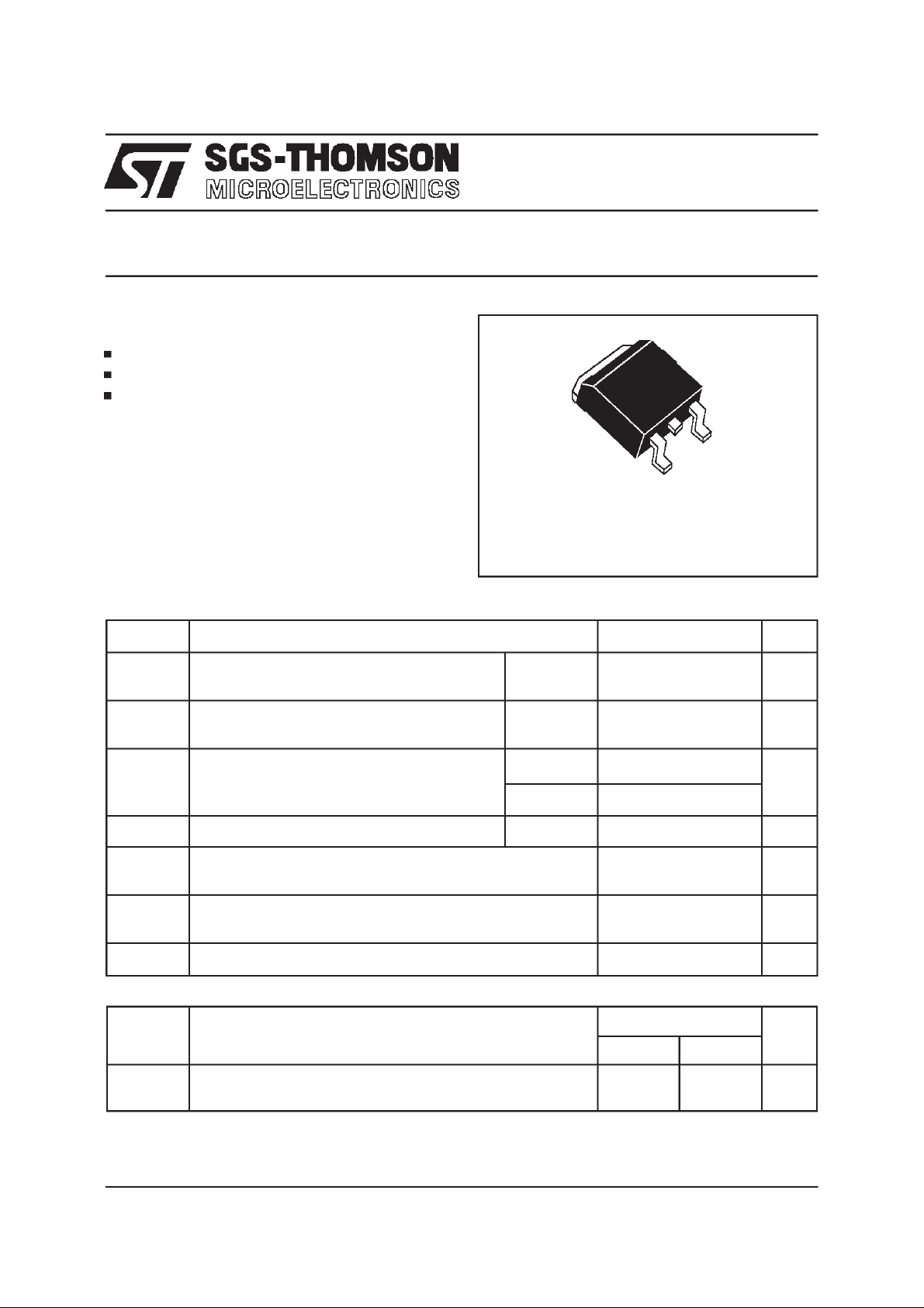
TN1625-G
SCR
HIGHSUR GECAPAB ILITY
A
HIGHON-STATECURRENT
HIGHSTABILITYAND RELIABILITY
DESCRIPTION
A
G
The TN1625series ofSilicon ControlledRectifiers
uses a high performance glass passivated tech-
K
nology.
This SCR is designed for power supplies up to
400Hzonresistiveor inductiveload.
D
2
PAK
ABSOLUTE MAXIMUM RATINGS
Symbol Parameter Value Unit
I
T(RMS)
RMSon-statecurrent
Tc=110°C16 A
(180°conductionangle)
I
T(AV)
Averageon-statecurrent
Tc=110°C10 A
(180°conductionangle)
I
TSM
2
tI
I
Nonrepetitive surgepeak on-statecurrent tp= 8.3 ms 199 A
(Tjinitial = 25°C)
2
t Valuefor fusing tp = 10ms 180 A2s
tp= 10 ms 190
dI/dt Criticalrate of riseof on-statecurrent
I
=100 mA dIG/dt =1 A/µs.
G
T
stg
T
j
Storagejunctiontemperaturerange
Operatingjunctiontemperaturerange
100 A/µs
- 40to+ 150
- 40to+ 125
Tl Maximumtemperaturefor solderingduring 10 s 260 °C
TN1625-
Symbol Parameter
600G 800G
V
DRM
V
RRM
January 1998- Ed: 4
Repetitivepeak off-statevoltage
Tj = 125°C
600 800 V
°C
Unit
1/5
Page 2
TN1625-G
THERMALRESISTANCES
Symbol Parameter Value Unit
2
Rth(j-a) Junctionto ambient(S=1cm
Rth(j-c) Junctionto case forD.C 1.1 °C/W
GATECHARACTERISTICS
P
=1W PGM=10 W (tp =20µs) IGM= 4 A(tp = 20µs) V
G (AV)
ELECTRICALCHARACTERISTICS
Symbol TestConditions Type Value Unit
)45
=5V
RGM
°
C/W
I
GT
V
GT
V
GD
I
H
I
L
V
TM
I
DRM
I
RRM
dV/dt V
VD=12V (DC) RL=33
Ω
Tj=25°C MIN 3 mA
MAX 25
VD=12V (DC) RL=33Ω
VD=V
DRMRL
=3.3kΩ Tj= 125°C MIN 0.2 V
Tj=25°C MAX 1.3 V
IT= 100mA Gateopen Tj=25°C MAX 40 mA
IG=1.2 I
GT
Tj=25°C MAX 60 mA
ITM= 32A tp=380µs Tj=25°C MAX 1.5 V
VD=V
VR=V
=67%V
D
DRM
RRM
Gateopen Tj=125°C MIN 500 V/µs
DRM
Tj=25°C MAX 5 µA
Tj= 125°C MAX 2 mA
ORDERINGINFORMATION
TN 16 25 - 600 G
SCR
CURRENT
2/5
Add”-TR” suffixfor Tape &Reelshipment
SENSITIVITY
PACKAGES:
G: D
VOLTAGE
2
PAK
Page 3

TN1625-G
Fig. 1:
Maximum average power dissipation ver-
susaverage on-statecurrent.
P(W)
16
14
12
10
α=30°
α=180°
α=120°
α=90°
α=60°
D.C.
8
6
4
2
0
0246810121416
Fig. 3:
Averageand D.C. on-state current versus
I (A)T(AV)
casetemperature.
T(AV)
I (A)
18
16
14
12
10
8
6
4
2
0
0 25 50 75 100 125
D.C.
α=180°
Tcase(°C)
Fig. 2 :
Correlation betweenmaximum average
power dissipationandmaximum allowabletem-
peratures (T
amb
and T
) for diffe rentthermal
case
resistances heatsink+contact.
P(W) Tcase (°C)
16
14
12
10
8
6
4
2
0
0 20 40 60 80 100 120 140
Fig. 4:
α=180°
Tamb(°C)
Relative variation of thermal impedance
Rth=0°C/WRth=2°C/WRth=4°C/WRth=6°C/W
110
115
120
125
versuspulseduration.
K=[Zth/Rth]
1.00
Zth(j-c)
Zth(j-a)
0.10
tp(s)
0.01
1E-3 1E-2 1E-1 1E+0 1E+1 1E+2 5E+2
Fig.5:
Relativevariationofgatetriggercurrentand
holdingcurrentversusjunctiontemperature.
I ,I [Tj]/I ,I [Tj=25°C]GT H GT H
2.5
2.0
1.5
1.0
0.5
0.0
IGT
IH
Tj(°C)
-40 -20 0 20 40 60 80 100 120 140
Fig. 6:
Non repetitive surge peak on-statecurrent
versusnumberof cycles.
I (A)
TSM
200
Tj initial=25°C
160
120
80
40
0
1 10 100 1000
Number of cycles
F=50Hz
3/5
Page 4

TN1625-G
Fig. 7: Non repetitive surge peak on-state current
fora sinusoidalpulsewith widthtp<10ms,andcorrespondingvalueof I
I
(A),I t(A s)
TSM
1000
500
200
100
12 510
Fig.9:
I t
Thermalresistancejunctionto ambientver-
2
t.
Tj initial=25°C
TSM
I
tp(ms)
suscoppersurfaceundertab (Epoxy printed circuit
boardFR4, copperthickness:35µm).
Rth(j-a) (°C/W)
80
70
60
50
40
30
20
10
0
0 4 8 12 16 20 24 28 32 36 40
S(Cu) (cm )
Fig.8:On-statecharacteristics(maximumvalues).
I (A)
TM
200
100
10
Tj=Tj max.
Tj=25°C
Tj max.:
Vto=0.77V
Rt=23mΩ
V (V)TM
1
012345
Fig.10:
Typicalreflow solderingheatprofile,either
formounting onFR4 or metal-backedboards.
T(°C)
250
200
150
100
50
0
0 40 80 120 160 200 240 280 320 360
Epoxy FR4
board
Metal-backed
245°C
215°C
board
t (s)
4/5
Page 5

PACKAGEMECHANICALDATA
2
D
PAK
E
L2
L
L3
A1
B2
B
G
2.0 MIN.
FLAT ZONE
C2
TN1625-G
DIMENSIONS
A
REF.
A 4.30 4.60 0.169 0.181
A1 2.49 2.69 0.098 0.106
A2 0.03 0.23 0.001 0.009
D
B 0.70 0.93 0.027 0.037
B2 1.40 0.055
C 0.45 0.60 0.017 0.024
C
R
C2 1.21 1.36 0.047 0.054
D 8.95 9.35 0.352 0.368
E 10.00 10.28 0.393 0.405
G 4.88 5.28 0.192 0.208
A2
L 15.00 15.85 0.590 0.624
L2 1.27 1.40 0.050 0.055
V2
L3 1.40 1.75 0.055 0.069
R 0.40 0.016
V2 0° 8° 0° 8°
Millimeters Inches
Min. Typ. Max. Min. Typ. Max.
FOOTPRINT DIMENSIONS(in millimeters)
16.90
MARKING:
TN1625
x00G
10.30
8.90
Information furnished is believed to be accurate and reliable. However, SGS-THOMSON Microelectronics assumes no responsibility for the
consequences of use of such information nor forany infringement of patents or other rights of third partieswhich may result from its use. No
license is grantedby implication or otherwise under any patent or patentrights ofSGS-THOMSON Microelectronics.Specifications mentioned
in thispublicationare subjectto changewithout notice.This publication supersedes and replaces allinformation previously supplied.
SGS-THOMSON Microelectronicsproducts are not authorizedfor useas critical componentsin life supportdevices or systemswithoutexpress
written approval ofSGS-THOMSON Microelectronics.
1998 SGS-THOMSON Microelectronics - Printed in Italy -All rights reserved.
Australia - Brazil - Canada- China - France - Germany- Italy -Japan - Korea - Malaysia - Malta - Morocco
The Netherlands- Singapore - Spain - Sweden - Switzerland - Taiwan -Thailand - United Kingdom -U.S.A.
3.70
SGS-THOMSON MicroelectronicsGROUP OF COMPANIES
5.08
1.30
5/5
 Loading...