

Page 1

INTEGRATED CIRCUITS
TL431C, TL431AC, TL431I,
TL431AI, LM431AC
Adjustable precision shunt regulators
Product specification 1997 Feb 25
Page 2
Philips Semiconductors Product specification
Adjustable precision shunt regulators
DESCRIPTION
The TL431 and TL431A are 3-terminal adjustable shunt regulators
with specified thermal stability over applicable automotive and
commercial temperature ranges. The output voltage may be set to
any value between V
external resistors (see Figure 4). These devices have a typical
output impedance of 0.2Ω. Active output circuitry provides a very
sharp turn-on characteristic, making these devices excellent
replacements for zener diodes in many applications like on-board
regulation, adjustable power supplies and switching power supplies.
The TL431C and TL431AC are characterized for operation from
0°C to +70°C; the TL431I and TL431AI are characterized for
operation from –40°C to +85°C.
FEATURES
•Equivalent full-range temperature coefficient: 30ppm/°C
•0.2Ω typical output impedance
•Sink current capability: 1mA to 100mA
•Low output noise
•Adjustable output voltage: V
(approximately 2.5V) and 36V with two
REF
to 36V
REF
TL431C, TL431AC, TL431I,
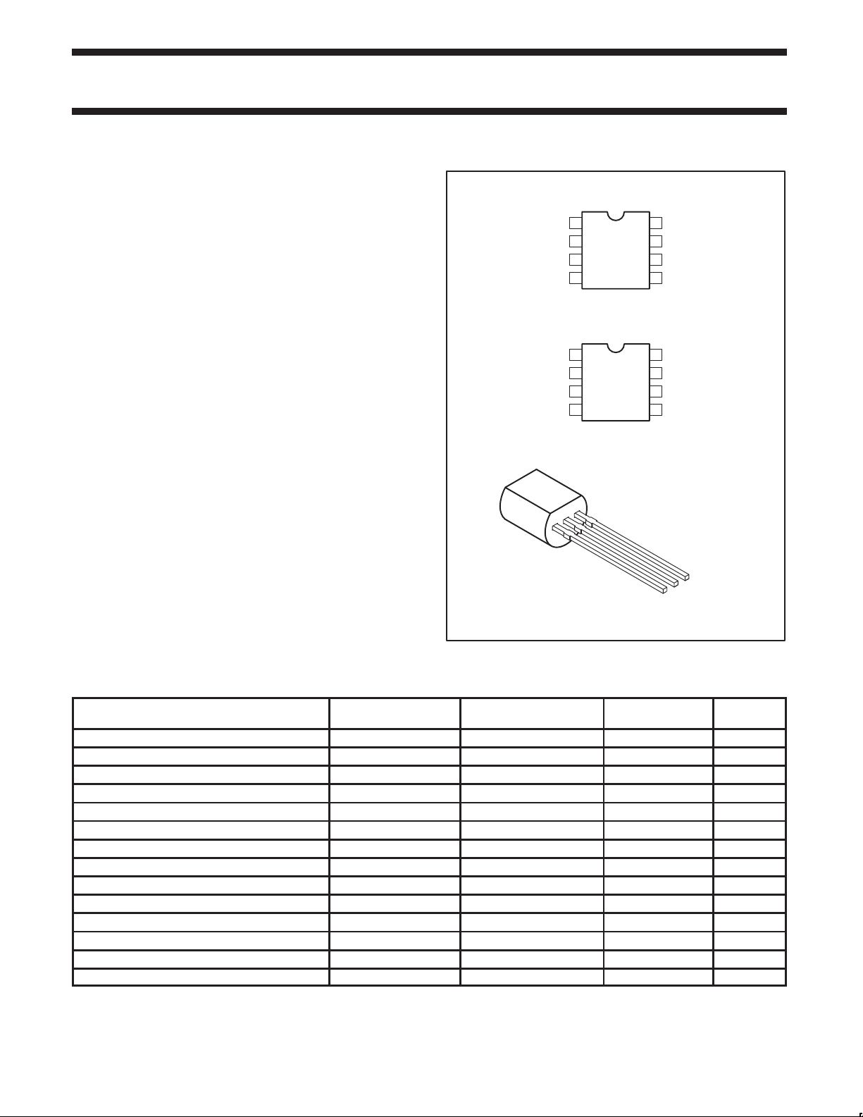
PIN CONFIGURATIONS
M, D Package
1
2
ANODE
3
ANODE
45
NC
N, P Package
1
2
NC
3
NC
45
NC
Z, LP, U Package
TL431AI, LM431AC
TOP VIEW
REF
8CATHODE
ANODE
7
ANODE
6
NC
SOT96-1
TOP VIEW
REF
8CATHODE
NC
7
ANODE
6
NC
SOT97-1
CATHODE
ANODE
SOT54
REF
SL01167
Figure 1. Pin Configuration
ORDERING INFORMATION
DESCRIPTION
3-Pin Plastic TO92
3-Pin Plastic TO92
3-Pin Plastic TO92
3-Pin Plastic TO92
3-Pin Plastic TO92
2
2
2
2
2
TEMPERATURE
RANGE
0°C to +70°C TL431CLP TL431CLPU SOT54
0°C to +70°C TL431ACLP TL431ACLPU SOT54
–40°C to +85°C TL431ILP TL431ILPU SOT54
–40°C to +85°C TL431AILP TL431AILPU SOT54
0°C to +70°C LM431ACZ LM431ACZU SOT54
8-Pin Plastic Small Outline (SO) package 0°C to +70°C TL431CD TL431CD SOT96-1
8-Pin Plastic Small Outline (SO) package –40°C to +85°C TL431ID TL431ID SOT96-1
8-Pin Plastic Small Outline (SO) package 0°C to +70°C TL431ACD TL431ACD SOT96-1
8-Pin Plastic Small Outline (SO) package –40°C to +85°C TL431AID TL431AID SOT96-1
8-Pin Plastic Small Outline (SO) package 0°C to +70°C LM431ACM LM431ACMD SOT96-1
8-Pin Plastic Dual In-Line package (DIP) 0°C to +70°C TL431CP TL431CPN SOT97-1
8-Pin Plastic Dual In-Line package (DIP) –40°C to +85°C TL431IP TL431IPN SOT97-1
8-Pin Plastic Dual In-Line package (DIP) 0°C to +70°C TL431ACP TL431ACPN SOT97-1
8-Pin Plastic Dual In-Line package (DIP) –40°C to +85°C TL431AIP TL431AIPN SOT97-1
NOTE:
1. SYMBOL INFORMATION: Parts will be marked with product name including temperature and electrical grade desginators, but not the
package identifier.
2. TO92 is normally shipped in bulk, i.e., in plastic bags (containing 1,000 parts), 5 bags per box. Tape and reel (or ammo box) is an option.
See page 15 for information.
INDUSTRY STANDARD
PART NUMBER
ORDER CODE DWG #
1997 Feb 25 853–1927 17795
2
Page 3
Philips Semiconductors Product specification
Adjustable precision shunt regulators
TL431C, TL431AC, TL431I,
TL431AI, LM431AC
ABSOLUTE MAXIMUM RATINGS
SYMBOL PARAMETER RATING UNITS
V
KA
T
amb
T
STG
NOTE:
1. Voltage values are with respect to the anode terminal unless otherwise noted.
RECOMMENDED OPERATING CONDITIONS
SYMBOL PARAMETER MIN MAX UNITS
V
KA
I
K
Cathode voltage (see Note 1) 37 V
Continuous cathode current range –100 to +150 mA
Reference input current range 0.05 to 10 mA
Operating free-air temperature range
C suffix 0 to +70 °C
I suffix –40 to +85 °C
Temperature storage range –65 to 150 °C
Lead temperature 1.6mm (1/16 in.) from case for 10 sec: D or P pkgs 260 °C
Lead temperature 1.6mm (1/16 in.) from case for 60 sec: LP pkg 300 °C
Cathode voltage V
REF
36 V
Cathode current 1 100 mA
Table 1. Dissipation Rating Table – Free-Air Temperature
Package
Derating Factor Above T
= 25°C
amb
D 5.8mW/°C 725mW 464mW 429mW
LP 6.2mW/°C 775mW 496mW 403mW
P 8.0mW/°C 1000mW 640mW 520mW
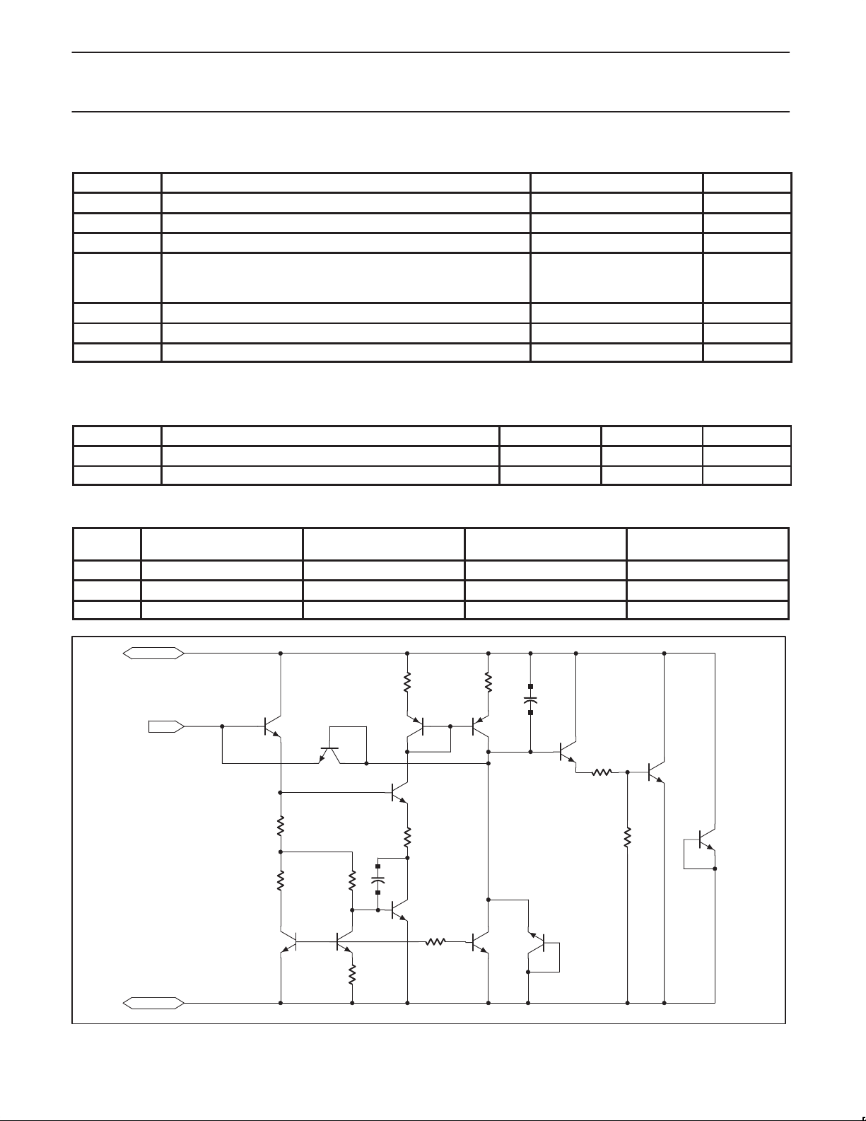
CATHODE
3.28K
R11
2.4K
Q5
R5
REF
T
Power Rating
QD6
R10
7.2K
amb
= 25°C
Q4
C2
20p
Q7
Q9
R4
800
R7
320
T
amb
Power Rating
R3
800
Q3
= 70°C
C1
20p
Q2
R2
150
R1
10K
T
= 85°C
amb
Power Rating
Q1
Qq1
1997 Feb 25
ANODE
Q11
Q10
R8
1000
800
R9
Figure 2. Equivalent Schematic
3
Q8
QD2
SL01188
Page 4
Philips Semiconductors Product specification
CKT
REF
in ut voltage to the change
Fig. 4
I
10mA
mV/V
CKT
REF
in ut voltage to the change
Fig. 4
I
10mA
mV/V
Adjustable precision shunt regulators
TL431C, TL431AC, TL431I,
TL431AI, LM431AC
DC ELECTRICAL CHARACTERISTICS
25°C free-air temperature, unless otherwise stated.
V
REF(dev)
LIMITS
LIMITS
, is defined as:
REF
SYMBOL PARAMETER
TEST
TEST CONDITIONS
TL431AC TL431C/LM431AC
MIN TYP MAX MIN TYP MAX
V
V
REF(dev)
V
V
I
REF
I
REF(dev)
I
MIN
I
OFF
| ZKA | Dynamic impedance
Reference input voltage Fig. 3 VKA = V
REF
Deviation of reference input
voltage over full
temperature range
Ratio of change in reference
REF
p
in cathode voltage
KA
3
Fig. 3
VKA = V
T
amb
=
K
, IK = 10mA 2470 2495 2520 2440 2495 2550 mV
REF
, IK = 10mA,
REF
= full range
∆VKA = 10V – V
2
REF
4 15 4 17 mV
–1.4 –2.7 –1.4 –2.7
∆VKA = 36V – 10V –1 –2 –1 –2
Reference input current Fig. 4 IK = 10mA, R1 = 10kΩ, R2 = ∞ 2 4 2 4 µA
Deviation of reference input
current over full temperature
3
range
Minimum cathode current
for regulation
Off-state cathode current Fig. 5 VKA = 36V, V
4
IK = 10mA, R1 = 10kΩ, R2 = ∞,
Fig. 4
Fig. 3 VKA = V
Fig. 3
= full range
T
amb
VKA = V
f ≤ 1kHz
REF
, IK = 1mA to 100mA,
REF
2
0.8 1.2 0.4 1.2 µA
0.4 0.6 0.4 1 mA
= 0 0.1 0.5 0.1 1 µA
REF
0.2 0.5 0.2 0.5 Ω
25°C free-air temperature, unless otherwise stated.
SYMBOL PARAMETER
TEST
TEST CONDITIONS
TL431AI TL431I
MIN TYP MAX MIN TYP MAX
V
V
REF(dev)
V
V
I
REF
I
REF(dev)
I
MIN
I
OFF
| ZKA | Dynamic impedance
Reference input voltage Fig. 3 VKA = V
REF
Deviation of reference input
voltage over full
temperature range
Ratio of change in reference
REF
p
in cathode voltage
KA
3
Fig. 3
VKA = V
T
amb
=
K
, IK = 10mA 2470 2495 2520 2440 2495 2550 mV
REF
, IK = 10mA,
REF
= full range
∆VKA = 10V – V
2
REF
5 25 5 30 mV
–1.4 –2.7 –1.4 –2.7
∆VKA = 36V – 10V –1 –2 –1 –2
Reference input current Fig. 4 IK = 10mA, R1 = 10kΩ, R2 = ∞ 2 4 2 4 µA
Deviation of reference input
current over full temperature
3
range
Minimum cathode current
for regulation
Off-state cathode current Fig. 5 VKA = 36V, V
4
IK = 10mA, R1 = 10kΩ, R2 = ∞,
Fig. 4
Fig. 3 VKA = V
Fig. 3
= full range
T
amb
VKA = V
f ≤ 1kHz
REF
, IK = 1mA to 100mA,
REF
2
0.8 2.5 0.8 2.5 µA
0.4 0.7 0.4 1 µA
= 0 0.1 0.5 0.1 1 µA
REF
0.2 0.5 0.2 0.5 Ω
NOTES:
2. Full temperature range is –40°C to +85°C for the TL431I and TL431AI, and 0°C to +70°C for the TL431C and TL431AC.
3. The deviation parameters V
the rated termperature range. The average full-range temperature coefficient of the reference input voltage, αV
V
V
| V
REF
|
ppm
degC
REF
REF(dev)
REF(dev)
at 25oC
T
amb
and I
10
are defined as the differences between the maximum and minimum values obtained over
REF(dev)
Max V
Min V
REF
REF
6
UNIT
UNIT
where ∆T
1997 Feb 25
is the rated operating free-air temperature range of the device.
amb
∆T
amb
4
Page 5
Philips Semiconductors Product specification
Adjustable precision shunt regulators
TL431C, TL431AC, TL431I,
TL431AI, LM431AC
can be positive or negative depending on whether minimum V
αV
REF
Example: Max V
REF
| +
| V
Because minimum V
4. The dynamic impedance is defined as:
= 2496mV at 30°C, Min V
REF
4mV
ǒ
2495mV
70oC
6
Ǔ
@ 10
+ 23ppmńoC
occurs at the lower temperature, the coefficient is positive.
REF
|Z
= 2492mV at 0°C, V
REF
V
| +
KA
I
KA
When the device is operating with two external resistors, (see Figure xx), the total dynamic impedance of the circuit is given by:
|ZȀ|+
V
[|ZKA|ǒ1 )
I
R1
R2
Ǔ
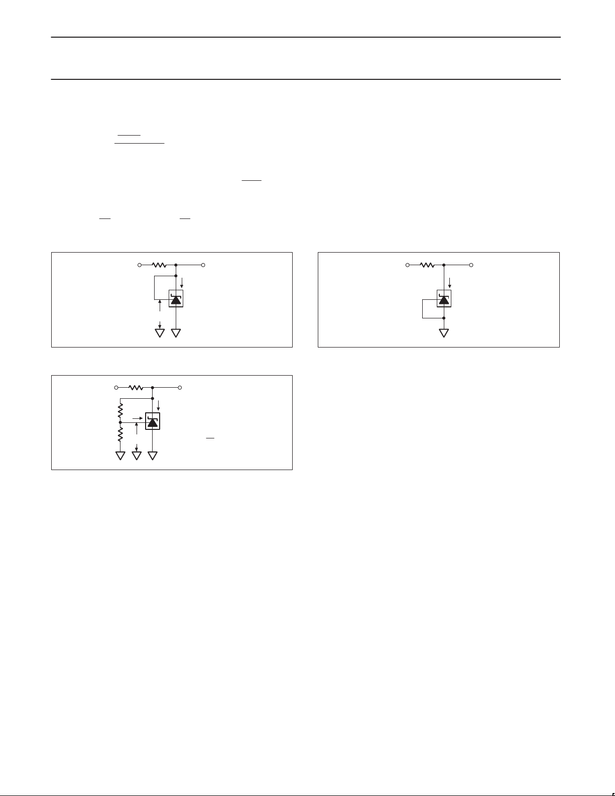
P ARAMETER MEASUREMENT INFORMATION
INPUT
V
ref
Figure 3. Test Circuit for VKA = V
V
KA
I
K
SL01177
ref
of maximum V
REF
= 2495mV at 25°C, DTA = 70°C for TL431C.
REF
, respectively, occurs at the lower temperature.
REF
INPUT V
Figure 5. Test Circuit for I
I
off
KA
SL01179
OFF
INPUT
R1
I
ref
R2
V
ref
I
K
VKA+ V
V
KA
ǒ
1 )
ref
Figure 4. Test Circuit for VKA > V
R1
Ǔ
) I
R1
ref
R2
SL01178
ref
1997 Feb 25
5
Page 6

Philips Semiconductors Product specification
Adjustable precision shunt regulators
2600
VKA = V
2580
2560
2540
2520
2500
2480
2460
2440
REFERENCE INPUT VOLTAGE – (mV)
2420
–
2400
ref
–50 –25 0 25 50 75 100 125
V
Figure 6. Reference Input Voltage vs. Temperature
150
125
100
75
50
25
0
–25
–50
CATHODE CURRENT – (mA)
–75
–100
Figure 7. Cathode Current vs. Cathode Voltage
ref
IK = 10mA
T
– TEMPERATURE – (°C)
amb
VKA = V
ref
T
= 25°C
amb
–2–10123
CATHODE VOLTAGE – (V)
V
= 2550mV
ref
V
= 2495mV
ref
V
= 2440mV
ref
SL01170
SL01171
TL431C, TL431AC, TL431I,
TL431AI, LM431AC
3.0
R1 = 10kΩ
R2 = ∞
2.5
= 10mA
I
K
2.0
1.5
1.0
0.5
REFERENCE INPUT CURRENT – ( A)µ
–
0
–75 –50 –25 0 25 50 75 100 125
ref
I
Figure 9. Reference Input Current vs. Temperature
90
VKA = 36V
80
= 0V
V
ref
70
60
50
40
30
20
10
OFF-STATE CATHODE CURRENT – (nA)
–
0
–75 –50 –25 0 25 50 75 100 125
off
I
Figure 10. Off-State Cathode Current vs. Temperature
– TEMPERATURE – (°C)
T
amb
– TEMPERATURE – (°C)
T
amb
SL01168
SL01169
800
VKA = V
ref
T
= 25°C
amb
600
400
200
CATHODE CURRENT – ( A)µ
0
–
K
I
–200
–10123
– CATHODE VOLTAGE – (V)
V
KA
Figure 8. Cathode Current vs. Cathode Voltage
1997 Feb 25
0
VKA = 3V TO 36V
–0.1
I
min
SL01172
–0.2
–0.3
–0.4
–0.5
–0.6
–0.7
d(Vref)/d(Vka) – (mV/V)
–0.8
–0.9
–1
–75 –50 –25 0 25 50 75 100 125
T
– TEMPERATURE – (°C)
amb
SL01173
Figure 11. Ratio of Delta Reference Voltage to
Delta Cathode Voltage over Temperature
6
Page 7

Philips Semiconductors Product specification
Adjustable precision shunt regulators
4
3
2
1
0
–1
–2
–3
Vn – INPUT NOISE VOLTAGE – Vµ
–4
012345678910
Equivalent Input Noise Voltage Over a 10-Second Period
19.1V
1kΩ
TL431C, TL431AC, TL431I,
TL431AI, LM431AC
t – TIME – (SECONDS)
500µF
√
910Ω
TL431
(DUT)
2000µF
400
350
300
250
820Ω
16Ω
0.1µF
IK = 10mA
= 25°C
T
amb
160kΩ
V
CC
TLE2027
A
V
EE
= 10V/mV
V
Test Circuit
16kΩ
Figure 12.
16kΩ
1µF
1µF
33kΩ
33kΩ
V
CC
V
EE
TLE2027
= 2V/V
A
V
22µF
1MΩ
CRO
SL01174
1997 Feb 25
200
Vn – NOISE VOLTAGE – nV/ Hz
150
100
10 100 1K 10K 100K
f–FREQUENCY–Hz
Figure 13. Equivalent Input Noise Voltage vs. Frequency
7
SL01180
Page 8

Philips Semiconductors Product specification
Adjustable precision shunt regulators
TYPICAL CHARACTERISTICS
7
6
5
4
3
2
1
INPUT AND OUTPUT VOLTAGE – V
0
100
90
80
01234567
T
= 25°C
amb
= V
AV
KA
KA
KA
= 10V
= 15V
ref
BVKA = 5V
CV
DV
t – TIME – µs
Pulse Response
UNSTABLE
< 5
V
KA
Figure 14. Pulse Response
TL431C, TL431AC, TL431I,
TL431AI, LM431AC
220Ω
PULSE
GENERATOR
f = 100kHz
50Ω
Test Circuit
B
C
OUTPUT
GND
SL01182
150Ω
I
K
V
L
BATT
70
60
50
40
CATHODE CURRENT – (mA)
–
K
I
30
20
10
0
0.001 0.01 0.1 1 10
STABLE STABLE
A
C
– LOAD CAPACITANCE – (µF)
L
UNSTABLE
V
< 10
KA
UNSTABLE VKA < 15V
D
UNSTABLE V
A
C
KA
Figure 15. Stability Boundary Conditions
Test Circuit for Curve A
I
R1 = 10kΩ
C
L
R2
K
150Ω
V
BATT
Test Circuit for Curves B, C, and D
SL01176
1997 Feb 25
8
Page 9

Philips Semiconductors Product specification
Adjustable precision shunt regulators
100
IK = 10mA
= 25°C
T
amb
10
1
KA
|Z | – REFERENCE IMPEDANCE – Ω
0.1
1K 10K 100K 1M 10M
f – FREQUENCY – Hz
Figure 16. Reference Impedance vs. Frequency
TL431C, TL431AC, TL431I,
TL431AI, LM431AC
1kΩ
50Ω
Test Circuit for Reference Impedance
OUTPUT
I
K
GND
SL01175
70
IK = 10mA
= 25°C
T
amb
60
50
40
30
20
Av – VOLTAGE AMPLIFICATION – dB
10
0
1K 10K 100K 1M 10M
FREQUENCY IN Hz
Figure 17. Small-Signal Voltage Amplification vs. Frequency
I
15kΩ
9µF
8.25kΩ
K
230Ω
Test Circuit for Voltage Amplification
OUTPUT
GND
SL01181
1997 Feb 25
9
Page 10

Philips Semiconductors Product specification
Adjustable precision shunt regulators
TYPICAL APPLICATIONS
V+
R1
R2
R1
OUT
ǒ
+
V
1 )
R2
Ǔ
Figure 18. Shunt Regulator
V+
V
OUT
V
IN
VTH = V
ref
Figure 19. Single-Supply Comparator with
Temperature-Compensated Threshold
V
OUT
V
ref
SL01183
V
< V
> V
V
IN
OUT
V+
ref
≈2.0V
ref
SL01184
TL431C, TL431AC, TL431I,
TL431AI, LM431AC
Ǔ
+ V
ref
CL
V
OUT
R1
R2
V
ref
be
R
CL
OUT
V+
R1
V
OUT
OUT
ǒ
+
1 )
Min = V
R2
ref
V
Figure 21. Series Pass Regulator
V+ I
V
I
+
OUT
R
Figure 22. Constant Current Source
SL01186
SL01187
V+
R1
OUT
ǒ
+
V
1 )
R2
Ǔ
V
OUT
R1
R2
V
ref
Figure 20. High Current Shunt Regulator
SL01185
V+ I
SINK
V
+
ref
R
S
I
SINK
R
S
Figure 23. Constant Current Sink
SL01189
1997 Feb 25
10
Page 11

Philips Semiconductors Product specification
Adjustable precision shunt regulators
TL431C, TL431AC, TL431I,
TL431AI, LM431AC
SO8: plastic small outline package; 8 leads; body width 3.9mm SOT96-1
1997 Feb 25
11
Page 12

Philips Semiconductors Product specification
Adjustable precision shunt regulators
TL431C, TL431AC, TL431I,
TL431AI, LM431AC
DIP8: plastic dual in-line package; 8 leads (300 mil) SOT97-1
1997 Feb 25
12
Page 13

Philips Semiconductors Product specification
Adjustable precision shunt regulators
4.2 max.
5.2 max.
4.8
max.
2.54
1.6
1
2
3
TL431C, TL431AC, TL431I,
TL431AI, LM431AC
SOT54
0.40
min.
12.7 min.
0.48
0.40
0.66
0.56
2.0 max.
(1)
Dimensions in mm.
(1) Terminal dimensions within this zone are uncontrolled to allow for flow of plastic and terminal irregularities.
SL01191
1997 Feb 25
13
Page 14

Philips Semiconductors Product specification
SYMBOL
DIMENSION
REMARKS
Adjustable precision shunt regulators
TL431C, TL431AC, TL431I,
TL431AI, LM431AC
TO-92 transistors on tape TO-92
P
A
1
A
H
2
H
1
H
0
L
F
1
P
F
2
F
2
P
0
D
0
(p)
W
2
W
0
W
1
W
T
∆h ∆h
t
1
t
SL01192
Table 2. Tape specification (TO-92 leaded types)
SPECIFICATIONS
MIN. NOM. MAX. TOL. UNIT
A
1
A Body height 4.8 5.2 – mm
T Body thickness 3.5 3.9 – mm
P Pitch of component – 12.7 – ±1 mm
P
0
P
2
F Distance between outer leads – 5.08 – +0.6/–0.2 mm
∆h Component alignment – 0 1 – mm
W Tape width – 18 – ±0.5 mm
W
0
W
1
W
2
H
0
H
1
L Length of snipped leads – – 11 – mm
D
0
t Total tape thickness – – 1.2 – mm
F1, F
H
2
(p) Pull-out force 6 – – – N
NOTE:
1. Measured over 20 devices.
Body width 4 – 4.8 – mm
Feed hole pitch – 12.7 – ±0.3 mm
Cumulative pitch error – – – ±0.1 mm Note 1
Feed hole center to component center – 6.35 – ±0.4 mm to be measured at bottom of clinch
Hold-down tape width – 6 – ±0.2 mm
Hole position – 9 – +0.7/–0.5 mm
Hold-down tape position – 0.5 – ±0.2 mm
Lead wire clinch height – 16.5 – ±0.5 mm
Component height – – 23.25 – mm
Feed hole diameter – 4 – ±0.2 mm
Lead-to-lead distance – – – +0.4/–0.2 mm
2
Clinch height – – – – mm
1997 Feb 25
14
Page 15

Philips Semiconductors Product specification
Adjustable precision shunt regulators
Tape splicing
Splice the carrier tape on the back and/or front so that the feed hole
pitch (P
) is maintained.
0
FEED
LABEL
FLAT SIDE OF TRANSISTOR AND ADHESIVE TAPE VISIBLE
CARRIER STRIP
FLAT SIDE
ADHESIVE TAPE
Figure 24. TO-92 Reel Styles
CATHODE
PIN
TL431C, TL431AC, TL431I,
TL431AI, LM431AC
Bulk packing
In addition to TO-92 on tape, TO-92 can also be delivered in bulk.
Products are packed in boxes in foil and plastic bags with 1,000
pieces to a bag and 5 bags to a box.
LABEL
CARRIER STRIP
ROUNDED
ADHESIVE TAPE
FEED
ROUNDED SIDE OF TRANSISTOR AND ADHESIVE TAPE VISIBLE
SPC F (Note 1)SPC T (Note 1)
SIDE
V
REF
PIN
SL01193
ADHESIVE TAPE ON TOP SIDE
FLAT SIDE
LABEL
In Ammo Pack, the parts are put on the tape
the same as in SPC T. However, depending
on which end of the Ammo Pack is opened,
the V
opened from the end marked with a “+”, the
OR Cathode pin may come first. If
REF
Cathode comes first.
Figure 25. TO-92 Ammo Pack Styles
NOTE:
1. Order SPC F, T or A depending on what is required.
FLAT SIDE OF TRANSISTOR
AND ADHESIVE TAPE VISIBLE
SPC A (Note 1)
CARRIER STRIP
SL01194
1997 Feb 25
15
Page 16

Philips Semiconductors Product specification
Adjustable precision shunt regulators
DEFINITIONS
TL431C, TL431AC, TL431I,
TL431AI, LM431AC
Data Sheet Identification Product Status Definition
Objective Specification
Preliminary Specification
Product Specification
Philips Semiconductors and Philips Electronics North America Corporation reserve the right to make changes, without notice, in the products,
including circuits, standard cells, and/or software, described or contained herein in order to improve design and/or performance. Philips
Semiconductors assumes no responsibility or liability for the use of any of these products, conveys no license or title under any patent, copyright,
or mask work right to these products, and makes no representations or warranties that these products are free from patent, copyright, or mask
work right infringement, unless otherwise specified. Applications that are described herein for any of these products are for illustrative purposes
only. Philips Semiconductors makes no representation or warranty that such applications will be suitable for the specified use without further testing
or modification.
LIFE SUPPORT APPLICA TIONS
Philips Semiconductors and Philips Electronics North America Corporation Products are not designed for use in life support appliances, devices,
or systems where malfunction of a Philips Semiconductors and Philips Electronics North America Corporation Product can reasonably be expected
to result in a personal injury. Philips Semiconductors and Philips Electronics North America Corporation customers using or selling Philips
Semiconductors and Philips Electronics North America Corporation Products for use in such applications do so at their own risk and agree to fully
indemnify Philips Semiconductors and Philips Electronics North America Corporation for any damages resulting from such improper use or sale.
Philips Semiconductors
811 East Arques Avenue
P.O. Box 3409
Sunnyvale, California 94088–3409
Telephone 800-234-7381
Formative or in Design
Preproduction Product
Full Production
This data sheet contains the design target or goal specifications for product development. Specifications
may change in any manner without notice.
This data sheet contains preliminary data, and supplementary data will be published at a later date. Philips
Semiconductors reserves the right to make changes at any time without notice in order to improve design
and supply the best possible product.
This data sheet contains Final Specifications. Philips Semiconductors reserves the right to make changes
at any time without notice, in order to improve design and supply the best possible product.
Copyright Philips Electronics North America Corporation 1997
All rights reserved. Printed in U.S.A.
1997 Feb 25
16
 Loading...