

Page 1
AIC431/TL431A/TL431
Adjustable Precision Shunt Regulators
Analog Integrations Corporation 4F, 9, Industry E. 9th Rd, Science Based Industrial Park, Hsinchu Taiwan, ROC
www.analog.com.tw
DS-431-06 May 31, 01 TEL: 886-3-5772500 FAX: 886-3-5772510 1
n
FEATURES
l Unconditionally Stable.
l Precision Reference Voltage.
AIC431 :2.495V ±0.5%
TL431A :2.495V ±1.0%
TL431 :2.495V ±1.6%
l Sink Current Capability: 200mA.
l Minimum Cathode Current for Regulation: 250µA.
l Equivalent Full-Range Temperature Coefficient:
50 ppm/°C.
l Fast Turn-On Response.
l Low Dynamic Output Impedance: 0.08Ω.
l Adjustable Output Voltage.
l Low Output Noise.
l Space Saving SOT-89, SOT-23, TO-92 and SO8
packages.
n
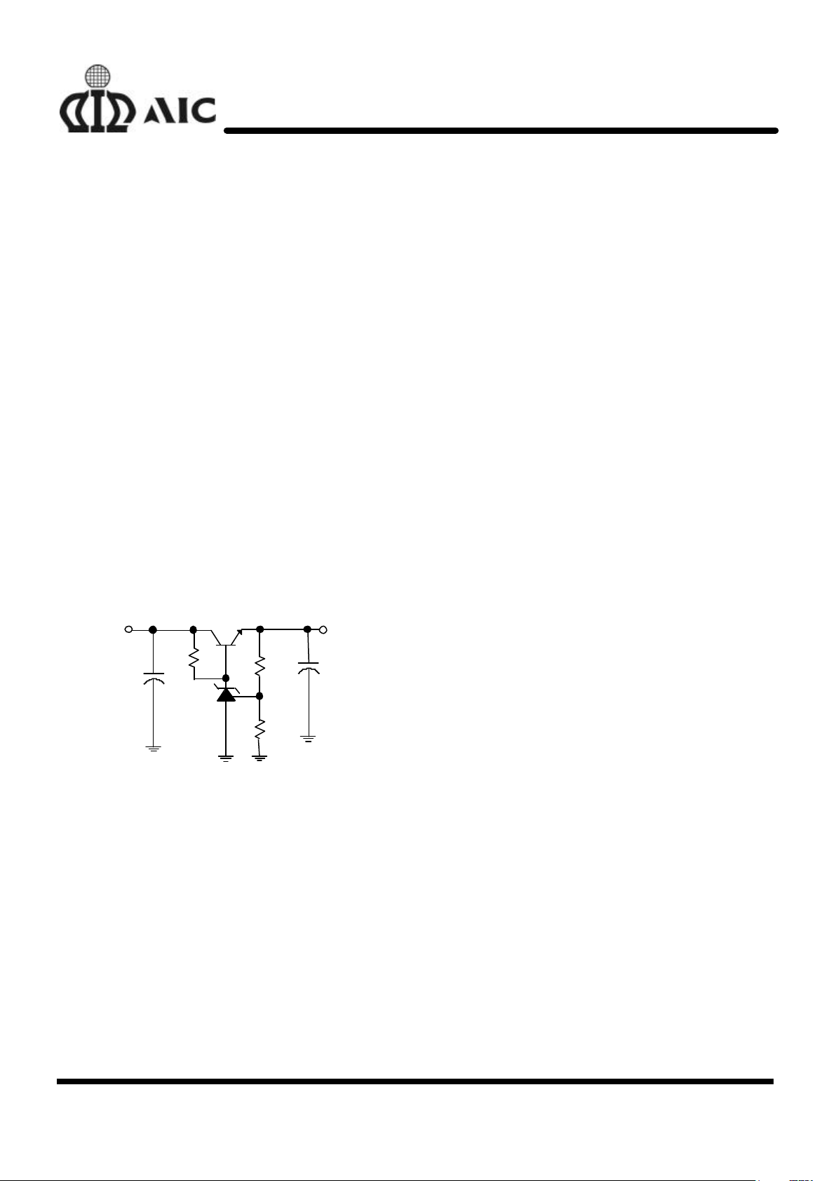
TYPICAL APPLICATION CIRCUIT
V
IN
AIC431
+
V
OUT
R1
R2
+
V
OUT
=(1+R1/R2)V
REF
Precision Regulator
n
DESCRIPTION
The AIC431/TL431A/TL431 are 3-terminal adjustable precision shunt regulators with guaranteed temperature stability over the applicable extended commercial temperature range.
The output voltage may be set at any level
greater than 2.495V (V
REF
) up to 30V merely
by selecting two external resistors that act as
a voltage divider network. These devices have
a typical output impedance of 0.08Ω. Active
output circuitry provides a very sharp turn-on
characteristics, making these devices excellent improved replacements for zener diodes
in many applications.
The precise ±0.5% reference voltage tolerance of the AIC431 makes it possible in
many applications to avoid the use of a variable resistor, consequently saving cost and
eliminating drift and reliability problems associated with it.
Page 2
AIC431/TL431A/TL431
2
n
ORDERING INFORMATION
ORDER NUMBER PIN CONFIGURATION
AIC431 CX
TL431A CX
TL431
CX
PACKAGING TYPE
S: SMALL OUTLINE
U: SOT-23
X: SOT-89
Z: TO-92
AIC431CX
TL431ACX
TL431CX
(SOT-89)
FRONT VIEW
1: VREF
2: ANODE
3: CATHODE
1
2
3
1 2 3
AIC431CZ
TL431ACZ
TL431CZ
(TO-92)
FRONT VIEW
1: VREF
2: ANODE
3: CATHODE
ANODE
REF
ANODE
NC
ANODE
ANODE
NC
CATHOD
1
3
4
2
8
6
5
7
AIC431CS
TL431ACS
TL431CS
(SO-8)
TOP VIEW
AIC431CUN
TL431ACUN
TL431CUN
(SOT-23)
FRONT VIEW
1: CATHODE
2: VREF
3: ANODE
1
3
2
AIC431CUS
TL431ACUS
TL431CUS
(SOT-23)
FRONT VIEW
1: VREF
2: CATHODE
3: ANODE
3
1
2
n
ABSOLUTE MAXIMUM RATINGS
Cathode Voltage ........……………...............……………..………...............................30V
Continuous Cathode Current ...................………….……...................... -10mA ~ 250mA
Reference Input Current Range .......…………........……..........…………………… 10mA
Operating Temperature Range .......………….........……….........……………. -40°C ~ 85°C
Lead Temperature .......…………..................………………..………………………. 260°C
Storage Temperature .......…………..................……………..…………….. -65°C ~ 150°C
Power Dissipation (Notes 1, 2) SOT-89 Package .........…………...... 0.80W
TO-92 Package ….......…………....... 0.78W
Note 1: T
J, max
= 150°C.
Note 2: Ratings apply to ambient temperature at 25°C.
Page 3
AIC431/TL431A/TL431
3
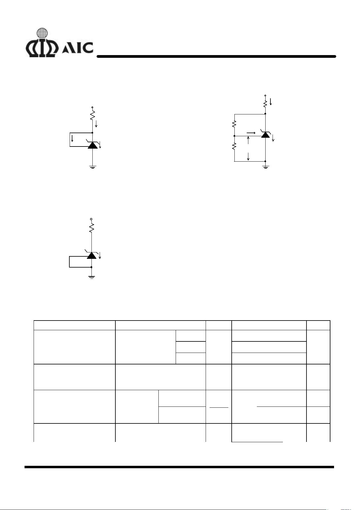
n
TEST CIRCUITS
V
REF
I
REF
I
Z
V
Z
I
L
IN
AIC431
R2
R1
V
REF
I
REFIZVZ
IN
I
L
AIC431
Note: VZ=V
REF
(1+R1/R2)+I
REF
xR1
Fig. 1 Test Circuit for VZ=V
REF
Fig. 2 Test circuit for VZ>V
REF
IN
VZ
IZ(OFF)
AIC431
Fig. 3 Test circuit for off-state Current
n
ELECTRICAL CHARACTERISTICS
(Ta=25°C, unless otherwise spec ified.)
PARAMETER TEST CONDITIONS
SYMBOL
MIN. TYP. MAX. UNIT
VZ=V
REF
, AIC431 2.482 2.495 2.508
IL =10mA (Fig. 1) TL431A 2.470 2.495 2.520
Reference Voltage
TL431
V
REF
2.455 2.495 2.535
V
Deviation of Reference
Input Voltage Over
Temperature (Note 3)
V
Z
= V
REF
, I
L
=10mA,
Ta = 0°C~ +85°C (Fig. 1)
V
DEV
9.0 20 mV
Ratio of the Change in Reference Voltage to
IZ=10mA ∆VZ=10V-V
REF
-0.5 -2.0 mV/V
the Change in Cathode voltage
(Fig. 2) ∆VZ=30V-10V
∆V
REF
∆V
Z
-0.35 -1.5 mV/V
Reference Input Current R1 =10KΩ, R2= ∞,
I
L
=10mA (Fig. 2)
I
REF
0.8 3.5 µA
Page 4

AIC431/TL431A/TL431
4
Deviation of Reference Input
Current over Temperature
R1 =10KΩ, R2= ∞,
I
L
=10mA
Ta =-20°C ~ +85°C (Fig. 2)
αI
REF
0.3 1.2 µA
Page 5

AIC431/TL431A/TL431
5
n
ELECTRICAL CHARACTERISTICS
(Continued)
PARAMETER TEST CONDITIONS
SYMBOL
MIN. TYP. MAX. UNIT
Minimum Cathode current for
Regulation
VZ=V
REF
(Fig. 1) I
Z(MIN)
0.25 0.5 mA
Off-State Current VZ=20V, V
REF
=0V (Fig. 3) I
Z(OFF)
0.1 1.0 µA
Dynamic Output Impedance
(Note 4)
VZ=V
REF
Frequency= 0Hz (Fig. 1)
R
Z
0.08 0.3 Ω
T
2
T
1
V
MAX
VDEV = VMAX-VMIN
V
MIN
TEMPERATURE
Note 3. Deviation of reference input voltage, V
DEV
, is defined as the maximum variation of the reference input
voltage over the full temperature range.
The average temperature coefficient of the reference input voltage, αV
REF
is defined as:
T1T2
10
C)25 (atV
V
T1T2
6
10
C)25 (atV
V-V
C
ppm
V
6
REF
DEV
REF
MINMAX
REF
−
°
±
=
−
°
±
=
°
∆
Where:
T
2−T1
=full temperature change.
αV
REF
can be positive or negative depending on
whether the slope is positive or negative.
Example: V
DEV
= 9.0mV, V
REF
= 2495mV,
T
2−T1
= 70°C, slope is negative.
C50ppm/V
C70
6
10
2495mV
9.0mV
REF °−=
=
°
α
Note 4. The dynamic output impedance, Rz, is de-
fined as:
RZ =
Z
ZV
I∆
∆
When the device is programmed with two external resistors, R1 and R2, (see Fig. 2), the dynamic output
impedance of the overall circuit, is defined as:
[
]
R2
R1
1Rz
Iz
Vz
zr +≅
∆
∆
=
n
TYPICAL PERFORMANCE CHARACTERISTICS
-1.0 -0.5 0.0 0.5 1.0 1.5 2.0 2.5 3.0
-600
-400
-200
0
200
400
600
800
1000
I
Z(MIN)
VZ =V
REF
TA =25°C
Cathode Current vs Cathode Voltage
Cathode Current (µA)
Cathode Voltage (V)
-40 -20 0 20 40 60 80 100 120
2.40
2.42
2.44
2.46
2.48
2.50
2.52
2.54
2.56
2.58
Reference Voltage
vs Temperature
VZ =V
REF
IZ =10mA
Reference
Voltage (V)
Temperature (
°
C)
V
REF
=2.535V
V
REF
=2.495V
V
REF
=2.455V
Page 6

AIC431/TL431A/TL431
6
n
TYPICAL PERFORMANCE CHARACTERISTICS (Continued )
-40
-20020406080100
120
0.70
0.75
0.80
0.85
0.90
0.95
1.00
1.05
1.10
1.15
1.20
Reference Input Current
vs Temperature
Reference
Input Current (
µ
A)
Temperature (
°
C)
R1=10K
Ω
R2=∞
IZ=10mA
-40 -20 0 20 40 60 80 100 120
0.00
0.04
0.08
0.12
0.16
0.20
0.24
0.28
VZ=V
REF
IZ=1mA to100mA
F <1KHz
Dynamic Impedance vs Temperature
Dynamic
Impedance (
Ω)Temperature (
°
C)
0510152025303540
-6-5-4-3-2-10
Change in Reference Voltage
vs Cathode Voltage
Change
in
Reference
Voltage (mV)
Cathode Voltage (V)
IZ =10mA
TA =25°C
-40
-20020406080100
120
0.0
0.5
1.0
1.5
2.0
2.5
Off-State Cathode Current vs Temperature
Off-State Cathode Current (µA)
Temperature (°C)
V
REF
=0V
VZ=30V
10
1001k10k
100k1M10M
-10
01020304050607080
Av
IZ =10mA
TA=25°C
Small Signal Voltage Amplification vs Frequency
Small Signal Voltage Amplification
Frequency (Hz)
R1
10K
R
250
+
V
IN
C
IN
47µF
V1
AIC431
Output
Test Circuit For Frequency Response
Page 7

AIC431/TL431A/TL431
7
n
TYPICAL PERFORMANCE CHARACTERISTICS (Continued )
Pulse Response
Input
Output
RA
50
RB
220
AIC431
OUTPUT
Pulse
Generator
f=100kHz
Test Circuit For Pulse Respnose
1E-4 1E-3 0.01 0.1 1 10
0
20
40
60
80
100
Stability Boundary Conditions
Cathode Current (mA)
Load Capacitance (µF)
VZ=V
REF
Stable
Stable
C
L
VIN
R
150
AIC431
VZ
The areas between the curves represent condition that Test Circuit for Stability Boundary Conditions
may cause the device oscillate
1K10K100K1M
0.1110
Iz=10mA
TA=25°C
Dynamic impedance vs. Frequency
Dynamic
Impedance (
Ω)Frequency
(Hz)
R1
50
+
AC
3V
R2
50
AIC431
GND
Output
+
Page 8

AIC431/TL431A/TL431
8
n
SYMBOL
n
BLOCK DIAGRAM
ANODE (A)
REF (R)
CATHODE (C)
AIC431
ANODE (A)
CATHODE (C)
REF (R)
+
-
2.495V
n
APPLICATION EXAMPLES
V
IN
R1A
R2A
R1B
R2B
AIC431
AIC431
R
ON
OFF
C
V
IN
+
AIC431
LED on when Low Limit<VIN< High Limit
Low Limit ≅ V
REF
(1+R1B/R2B) Delay=R x C x
ln (
V
V V
IN
IN REF−
)
High Limit ≅ V
REF
(1+R1A/R2A)
Fig. 4 Voltage Monitor Fig. 5 Delay Timer
R
CL
I
OUT
V
IN
AIC431
R
V
IN
S
I
OUT
AIC431
I
OUT=VREF
/ R
CL
I
OUT=VREF /RS
Fig. 6 Current Limiter or Current Source Fig. 7 Constant-Current Sink
Page 9

AIC431/TL431A/TL431
9
n
APPLICATION EXAMPLES (Continued)
V
OUT
R1
R2
V
IN
AIC431
V
IN
R1
R2
V
OUT
FUSE
AIC431
V
OUT
≅ (1+R1/R2) x V
REF
V
LIMIT
≅ (1+R1/R2) x V
REF
Fig 8. Higher-Current Shunt Regulator Fig 9. Crow Bar
R1A
R2A
R2B
R1B
V
IN
Output ON when
Low Limit <V
IN
< High Limit
+
V
BE
AIC431
AIC431
Low Limit≅ V
REF
( 1+ R1B/ R2B )+ V
BE
High Limit ≅ V
REF
( 1+ R1A/ R2A )
Fig 10. Over-Voltage/Under-Voltage Protection Circuit
Page 10

AIC431/TL431A/TL431
10
n
PHYSICAL DIMENSIONS
l 8 LEAD PLASTIC SO (unit: mm)
SYMBOL MIN MAX
A 1.35 1.75
A1 0.10 0.25
B 0.33 0.51
C 0.19 0.25
D 4.80 5.00
E 3.80 4.00
e 1.27(TYP)
H 5.80 6.20
L 0.40 1.27
D
H
e
A
B
A1
C
E
L
l SOT-23 (unit: mm)
SYMBOL MIN MAX
A 1.00 1.30
A1 — 0.10
A2 0.70 0.90
b 0.35 0.50
C 0.10 0.25
D 2.70 3.10
E 1.40 1.80
e 1.90 (TYP)
H 2.60 3.00
L 0.37 —
H
A1
AA2b
θ
1
L
C
D
E
e
θ1
1° 9°
l SOT-23 MARKING
Part No. Marking Part No. Marking
AIC431CUN AC1N AIC431CUS AC1S
TL431CUN AC2N TL431CUS AC2S
TL431ACUN AC3N TL431ACUS AC3S
Page 11

AIC431/TL431A/TL431
11
n
PHYSICAL DIMENSIONS (Continued)
l SOT-89 (unit: mm)
SYMBOL MIN MAX
A 1.40 1.60
B 0.36 0.48
C 0.35 0.44
D 4.40 4.60
D1 1.62 1.83
E 2.29 2.60
e 1.50 (TYP.)
e1 3.00 (TYP.)
H 3.94 4.25
B
e
H
e1
D
D1
A
C
L
E
L 0.89 1.20
l SOT-89 MARKING
Part No. Marking
AIC431CX AC01B
TL431CX AC02B
TL431ACX AC03B
l TO-92 (unit: mm)
SYMBOL MIN MAX
A 4.32 5.33
C 0.38 (TYP.)
D 4.40 5.20
E 3.17 4.20
e1 1.27 (TYP.)
A
L
e1
D
C
E
L 12.7 -
 Loading...