

Datasheet TL431IN, TL431ID, TL431CZ, TL431IZ, TL431AIZ Datasheet (SGS Thomson Microelectronics)
...Page 1
PROGRAMMABLE VOLTAGE REFERENCE
.
ADJUSTABLE OUTPUTVOLTAGE :
2.5 to 36V
.
SINK CURRENTCAPABILITY :1 to 100mA
.
TYPICALOUTPUT IMPEDANCE: 0.22Ω
.
1%AND 2% VOLTAGEPRECISION
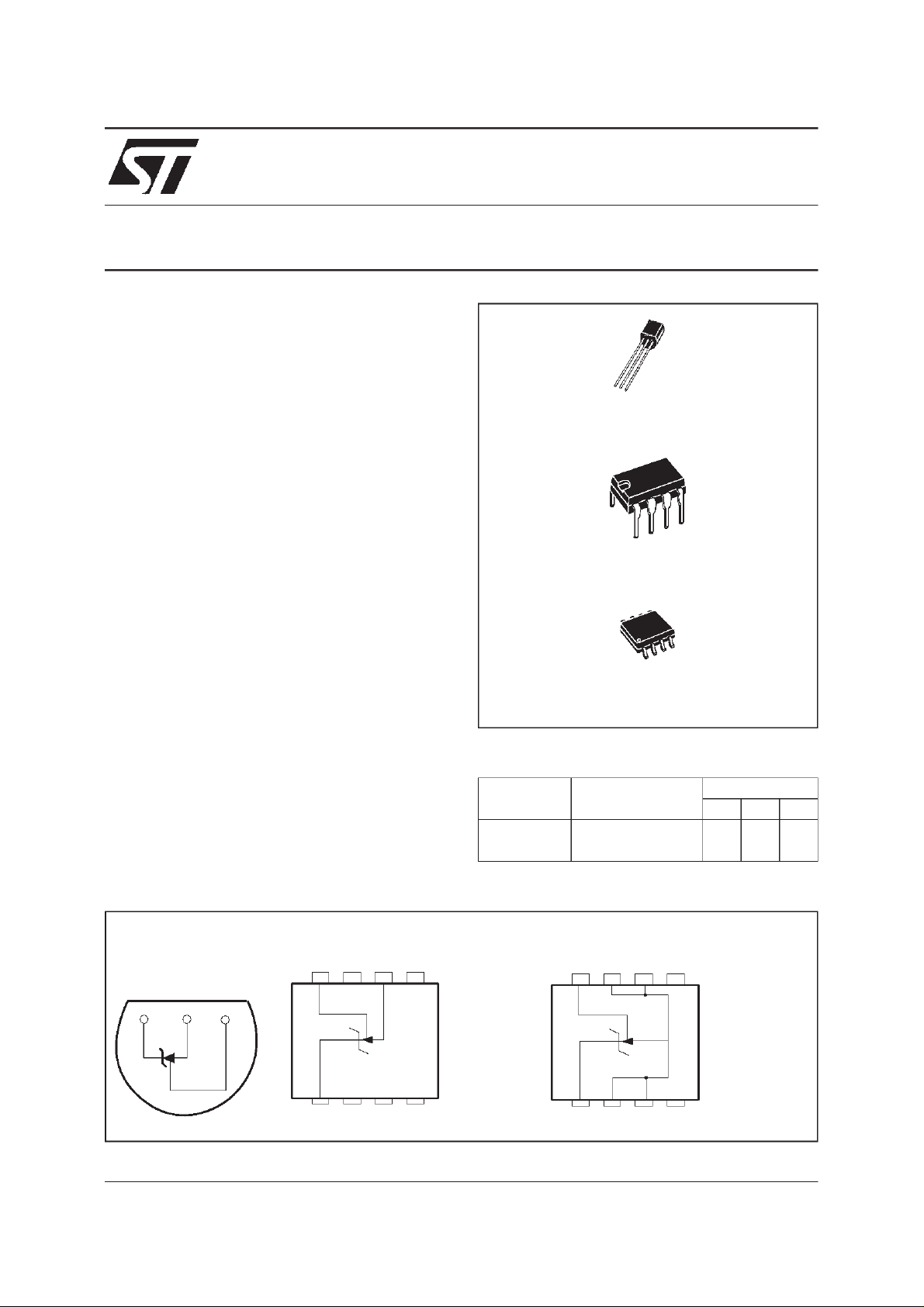
TL431
Z
TO92
(Plastic Package)
N
DIP8
(Plastic Package)
DESCRIPTION
The TL431is a programmableshuntvoltagereference with guaranteed temperature stability over
the entire temperature range of operation.
The output voltage may be set to any value between V
externalresistors.
The TL431operateswithawide currentrangefrom
1 to 100mA with a typical dynamic impedance of
0.22Ω.
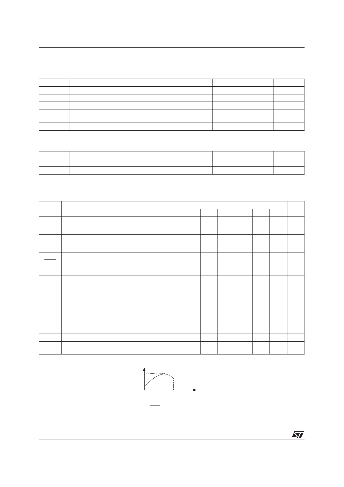
PIN CONNECTIONS
Cathode Anode Reference
(approximately2.5V) and 36Vwith two
ref
TO92
(Topview)
123
DIP8
(Top view)
8765
1234
(Batwing Plastic Micropackage)
ORDER CODES
Part number Temperature Range
o
TL431C/AC 0
TL431I/AI -40
1 - Cathode
2 - N.C.
3 - N.C.
4 - N.C.
5 - N.C.
6 -Anode
7 - N.C.
8 - Reference
C, +70oC •••
o
C, +105oC •••
SO8
(Top view)
8765
1234
D
SO8
Package
ZND
1 - Cathode
2 -Anode
3 -Anode
4 - N.C.
5 - N.C.
6 -Anode
7 -Anode
8 - Reference
November 1998
1/9
Page 2
TL431
ABSOLUTE MAXIMUM RATINGS
Symbol Parameter Value Unit
V
KA
I
K
I
ref
T
oper
T
stg
OPERATING CONDITIONS
Symbol Parameter Value Unit
V
KA
I
K
ELECTRICALCHARACTERISTICS
=25oC (unless otherwisespecified)
T
amb
Symbol Parameter
V
ref
∆V
ref
∆V
ref
∆V
KA
Iref Reference InputCurrent - (figure 2)
∆I
ref
I
min
I
off
| Dynamic Impedance - (figure 1, note 2)
|Z
KA
Cathode to Anode Voltage 37 V
Continuous Cathode Current Range -100 to +150 mA
Reference Input Current Range -0.05 to +10 mA
Operating Free-air Temperature Range TL431C/AC
TL431I/AI
0 to +70
-40 to +105
Storage Temperature Range -65 to +150
Cathode to Anode Voltage V
to 36 V
ref
Cathode Current 1 to 100 mA
TL431C TL431AC
Min. Typ. Max. Min. Typ. Max.
Reference InputVoltage - (figure1)
V
KA=Vref,IK
= 10mA T
≤ T
T
min.
amb
≤ T
max.
amb
=25oC
2.44
2.423
2.495 2.55
2.567
2.47
2.453
2.495 2.52
2.537
Reference InputVoltage Deviation Over
Temperature Range - (figure 1, note1)
V
KA=Vref,IK=
10mA,T
min.
≤ T
amb
≤ T
max.
317 315
Ratio of Change in Reference Input Voltage to
Change in Cathode to Anode Voltage - (figure 2)
=10mA ∆VKA= 10V to V
I
K
= 10mA, R1=10kΩ,R2=∞
I
K
∆VKA= 36V to 10V
=25oC
T
amb
≤ T
T
min.
amb
≤ T
ref
max.
-1.4-1-2.7
-2
1.8 4
5.2
-1.4-1-2.7
-2
1.8 4
5.2
Reference InputCurrent Deviation Over
Temperature Range - (figure 2)
= 10mA, R1=10kΩ,R2=∞
I
K
T
min.
≤ T
amb
≤ T
max.
0.4 1.2 0.4 1.2
Minimum Cathode Current for Regulation - (figure 1)
V
KA=Vref
0.5 1 0.5 0.6
Off-State CathodeCurrent - (figure 3) 2.6 1000 2.6 1000 nA
V
KA=Vref
, ∆IK= 1 to 100mA, f ≤ 1kHz 0.22 0.5 0.22 0.5
o
C
o
C
mV/V
Unit
V
mV
µA
µA
mA
Ω
Notes : 1. ∆V
2. The dynamic Impedance is defined as |ZKA| =
isdefined as the difference between the maximum and minimum values obtained over the full temperature
ref
range.
∆V
ref=Vrefmax.-Vrefmin
2/9
V
V
ref ma x.
re fmin.
T1
∆V
∆I
T2
KA
K
Temp era ture
Page 3
ELECTRICALCHARACTERISTICS
=25oC (unless otherwisespecified)
T
amb
Symbol Parameter
V
∆V
∆V
∆V
Iref Reference InputCurrent - (figure 2)
∆I
I
|Z
Reference InputVoltage - (figure1)
ref
ref
ref
KA
ref
min
I
off
| Dynamic Impedance - (figure 1, note 2)
KA
V
KA=Vref,IK
Reference InputVoltage Deviation Over
Temperature Range - (figure 1, note1)
V
KA=Vref,IK=
Ratio of Change in Reference Input Voltage to
Change in Cathode to Anode Voltage - (figure 2)
=10mA ∆VKA= 10V to V
I
K
= 10mA, R1=10kΩ,R2=∞
I
K
Reference InputCurrent Deviation Over
Temperature Range - (figure 2)
= 10mA, R1=10kΩ,R2=∞
I
K
Minimum Cathode Current for Regulation - (figure 1)
V
KA=Vref
Off-State CathodeCurrent - (figure 3) 2.6 1000 2.6 1000 nA
V
KA=Vref
= 10mA T
≤ T
T
min.
10mA,T
min.
∆VKA= 36V to 10V
=25oC
T
amb
≤ T
T
min.
≤ T
T
min.
, ∆IK= 1 to 100mA, f ≤ 1kHz 0.22 0.5 0.22 0.5
amb
≤ T
amb
amb
≤ T
amb
≤ T
≤ T
max.
≤ T
max.
max.
TL431
TL431I TL431AI
Min. Typ. Max. Min. Typ. Max.
=25oC
amb
max.
ref
2.44
2.41
2.495 2.55
2.58
2.47
2.44
2.495 2.52
730 730
-1.4-1-2.7
-1.4-1-2.7
-2
1.8 4
1.8 4
6.5
0.8 2.5 0.8 1.2
0.5 1 0.5 0.7
Unit
V
2.55
mV
mV/V
-2
µA
6.5
µA
mA
Ω
Notes : 1. ∆V
2. The dynamic Impedance is defined as |ZKA| =
isdefined as the difference between the maximum and minimum values obtained over the full temperature
ref
range.
∆V
=V
refmax.-Vrefmin
ref
V
ref ma x.
V
re fmin.
T1 T2
∆V
Temp era ture
KA
∆I
K
3/9
Page 4

TL431
2,58
2,56
2,54
2,52
2,5
2,48
Referencevoltage (V)
2,46
2,44
2,42
-40 -30 -20 -10 0 10 20 30 40 50 60 70 80 90 100
Temperature(°C)
Cathode current vs Cathode voltage
100
90
Reference voltagevs Temperature
80
70
60
50
40
30
20
10
0
Ika Cathodecurrent(mA)
-10
-20
-30
-40
-50
-2 -1 0 1 2 3
Vka=Vref
Ta=25°C
VkaCathodevoltage (V)
Average
2%range
1%range
Vka=Vref
Ik=10mA
Test circuit for Vka=Vref
Input
Ik=10mA
Vref
Cathode current vs Cathode voltage
2
1,5
1
0,5
0
-0,5
Ika CathodeCurrent (mA)
-1
-1,5
-2
-10123
VkaCathodevoltage(V)
Vka=Vref
Ta=25°C
Output
Vka
Reference inputcurrent vs temperature
1,2
1,1
1
0,9
0,8
Iref Referenceinputcurrent(µA)
0,7
0,6
-40 -30 -20 -10 0 10 20 30 40 50 60 70 80 90 100
Temperature(°C)
Ika=10mA
R1=10K
R2=inf
4/9
Rka (Ohms)
0,24
0,235
0,23
0,225
0,22
0,215
Rka - Static impedance vs Temperature
Vka=Vref
Ika =1 to 100mA
-40 -30 -20 -10 0 10 20 30 40 50 60 70 80 90 100
Temperature(°C)
Page 5

TL431
Off State cathode currentvs temperature
1,4
1,2
1
0,8
0,6
0,4
Ioff OffStatecathode current(µA)
0,2
0
-40-30-20-10 0 102030405060708090100
Gain(dB) Phase(°)
60
50
40
30
20
10
0
1 2 5 10 20 50 100 200 500 1,000
Vka=36V
Vref=0V
Temperature(°C)
Phase & Gain vs Frequency
Frequency(KHz)
Gain
Phase
Test circuit for Off-state current measurement
Input Vka=36V
Ioff
180
160
140
120
100
80
60
40
20
Test circuit for Phase & Gain measurements
10µF
Ik=10mA
Input
10µF
6.8K
4.3K
Vref
Output
6
Pulse response for Ik=1mA
5
4
3
2
1
Input& Output voltage(V)
0
-1
012345678910
Input
Output
Time(µs)
Vka=Vref
Ik=1mA
Ta=25°C
Test circuit for pulse response at Ik=1mA
ΩΩ
2.5K
Ik=1mA
Pulse
Generator
Intput
50ΩΩ
Output
5/9
Page 6

TL431
6
5
4
3
2
1
Input & Output voltage(V)
0
-1
012345678910
Input
Output
Time (µs)
Vka=Vref
Ik=10mA
Ta=25°C
Stabilityconditionsvs Capacitive loads
110
Pulse responsefor Ik=10mA
100
90
80
Stable
70
area
60
50
40
Cathodecurrent(µA)
30
20
10
0
1E-10 1E-9 1E-8 1E-7 0,000001 0,00001
Vka=Vref
Vka=5V
Vka=12V
Vka=24V
Capacitiveload(F)
Unstable
area
Stable
area
Test circuit for pulse response at Ik=10mA
250ΩΩ
Ik=10mA
Pulse
Generator
Intput
50ΩΩ
Testcircuit for Vka > Vref
Input
R1
R2
Ik
Iref
Vref
Vka
Vka =Vref . (1+R1/R2) + Iref . R1
Output
6/9
Page 7

PACKAGE MECHANICAL DATA
8 PINS - PLASTIC DIP
TL431
Dim.
A 3.32 0.131
a1 0.51 0.020
B 1.15 1.65 0.045 0.065
b 0.356 0.55 0.014 0.022
b1 0.204 0.304 0.008 0.012
D 10.92 0.430
E 7.95 9.75 0.313 0.384
e 2.54 0.100
e3 7.62 0.300
e4 7.62 0.300
F 6.6 0260
i 5.08 0.200
L 3.18 3.81 0.125 0.150
Z 1.52 0.060
Min. Typ. Max. Min. Typ. Max.
Millimeters Inches
7/9
Page 8

TL431
PACKAGE MECHANICAL DATA
8 PINS - BATWING PLASTIC MICROPACKAGE(SO)
Dimensions
A 1.75 0.069
a1 0.1 0.25 0.004 0.010
a2 1.65 0.065
a3 0.65 0.85 0.026 0.033
b 0.35 0.48 0.014 0.019
b1 0.19 0.25 0.007 0.010
C 0.25 0.5 0.010 0.020
c1 45
D 4.8 5.0 0.189 0.197
E 5.8 6.2 0.228 0.244
e 1.27 0.050
e3 3.81 0.150
F 3.8 4.0 0.150 0.157
L 0.4 1.27 0.016 0.050
M 0.6 0.024
S8
Min. Typ. Max. Min. Typ. Max.
Millimeters Inches
o
(typ.)
o
(max.)
8/9
Page 9

PACKAGE MECHANICAL DATA
3 PINS - PLASTIC PACKAGETO92
TL431
Dimensions
Min. Typ. Max. Min. Typ. Max.
Millimeters Inches
L 1.27 0.05
B 3.2 3.7 4.2 0.126 0.1457 0.1654
O1 4.45 5.00 5.2 0.1752 0.1969 0.2047
C 4.58 5.03 5.33 0.1803 0.198 0.2098
K 12.7 0.5
O2 0.407 0.5 0.508 0.016 0.0197 0.02
a 0.35 0.0138
Information furnished is believed to be accurate and reliable. However, STMicroelectronics assumes no responsibility for the
consequences of use of such information nor for any infringement of patents or otherrights of third parties which may result from
its use. No license is granted by implication or otherwise under any patent or patent rights of STMicroelectronics. Specifications
mentioned in this publi cation are subject to change without notice. This publication supersedes and replaces all information
previously supplied.STMicroelectronics products arenotauthorized for useas critical components inlife support devicesor systems
without express writtenapprovalof STMicroelectronics.
Australia - Brazil - Canada - China - France - Germany - Italy - Japan - Korea- Malaysia - Malta - Mexico- Morocco
The Netherlands- Singapore - Spain - Sweden - Switzerland - Taiwan - Thailand - United Kingdom - U.S.A.
The STlogo is a trademark of STMicroelectronics
1998 STMicroelectronics – Printed in Italy – All Rights Reserved
STMicroelectronicsGROUP OF COMPANIES
http://www.st.com
9/9
 Loading...