

Page 1
BIDIRECTIONAL THYRISTOR OVERVOLTAGE PROTECTORS
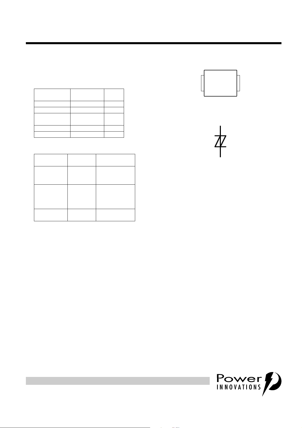
device symbol
OVERVOLTAGE PROTECTOR FOR ADSL MODEMS & SPLITTERS
●
Matched to POTS + ADSL Voltages
- W orking Voltage, V
- Protection Voltage, V
●
High FCC, Bellcore & ITU Surge Ratings
WAV E SHAP E STANDARD
2/10 µs GR-1089-CORE 500
10/160 µs FCC Part 68 250
10/700 µs
10/560 µs FCC Part 68 160
10/1000 µs GR-1089-CORE 100
●
High UL 1950, Bellcore & ITU AC Capability
STANDARD
UL 1950
(ANNEX NAC)
GR-1089-CORE
ITU-T K20/21
ITU-T K20/21
FCC Part 68
APPLIED AC
A RMS
40
7
2.2
60
30
15
2.2
23
1
. . . . . . . . . . . . .290 V
DRM
. . . . . . . . . . . .360 V
(BO)
I
TSP
A
200
‘4360 I
T(OV)M
s
0.04
4.2
SURVIVES
0.015
0.08
0.48
SURVIVES
0.15
SURVIVES
LIMIT
TISP4360H3BJ
SMBJ PACKAGE
(TOP VIEW)
12
T
R
Terminals T and R correspond to the
alternative line designators of A and B
●
Large creepage distance . . . . . . . . . 2.54 mm
●
Low Capacitance . . . . . . . . . . . . 24 pF @ 50 V
. . . . . . . . . . . . . .70 pF @ 0
T(A)R(B)
MDXXBG
SD4XAA
JUNE 1999Copyright © 1999, Power Innovations Limited, UK
description
The TISP4360H3BJ is d esigned to li mit overvoltages on eq uipment use d for telephone lines carr ying POTS
(Plain Old Telephone System) and ADSL (Asymmetrical Digital Subscriber Line) signals. TISP4360H3BJ a.c.
overload limits are specified for designers to select the correct overcurrent protectors to meet safety
requirements, e.g. UL 1950.
The protector consists of a symmetrical voltage-triggered bidirectional thyristor. Overvoltages are initially
clipped by breakdown clamping. If suffi cien t curre nt is available from the overvoltage, the breakdown voltage
will rise to the breakover level, which causes t he device to switch into a low-voltage on-stat e conditio n. This
switching action removes the high voltage str ess f rom th e following circuitry and caus es the cur rent res ultin g
from the overvoltage to be safely diverted through the protector. The high holding (switch off) current prevents
d.c. latchup as the diverted current subsides.
The TISP4360H3BJ is gu aranteed to voltage limit and withstand the listed inter national lightning surges i n
both polaritie s. This high (H ) curre nt prote ction device is in a plas tic SM BJ package (JE DEC DO-214 AA wit h
J-bend leads) and supplied in embossed carrier reel pack. For alternative voltage and holding current values,
consult the factory.
PRODUCT INFORMATION
Information is current as of publication date. Produc ts conform to specifications in accordance
with the terms of Power Innovations standard warranty. Production processing does not
necessarily include testing of all parameters.
1
Page 2

TISP4360H3BJ
BIDIRECTIONAL THYRISTOR OVERVOLTAGE PROTECTORS
JUNE 1999
T
absolute maximum ratings,
Repetitive peak off-state voltage, (see Note 1) V
Non-repetitive peak on-state pulse current (see Notes 2, 3 and 4)
2/10 µs (GR-1089-CORE, 2/10 µs voltage wave shape) 500
8/20 µs (IEC 61000-4-5, 1.2/50 µs voltage, 8/20 current combination wave generator) 300
10/160 µs (FCC Part 68, 10/160 µs voltage wave shape) 250
5/200 µs (VDE 0433, 10/700 µs voltage wave shape) 220
0.2/310 µs (I3124, 0.5/700 µs voltage wave shape) 200
5/310 µs (ITU-T K20/21, 10/700 µs voltage wave shape) 200
5/310 µs (FTZ R12, 10/700 µs voltage wave shape) 200
10/560 µs (FCC Part 68, 10/560 µs voltage wave shape) 160
10/1000 µs (GR-1089-CORE, 10/1000 µs voltage wave shape) 100
Non-repetitive peak on-state current (see Notes 2, 3 and 5)
20 ms (50 Hz) full sine wave
16.7 ms (60 Hz) full sine wave
1000 s 50 Hz/60 Hz a.c.
Maximum overload on-state current without open circuit, 50 Hz/60 Hz a.c.
0.015 s
0.04 s
0.08 s
0.15 s
0.48 s
4.2 s
Initial rate of rise of on-state current, Exponential current ramp, Maximum ramp value < 200 A di
Junction temperature T
Storage temperature range T
= 25°C (unless otherwise noted)
A
RATING SYMBOL VALUE UNIT
DRM
I
TSP
I
TSM
I
T(OV)M
/dt 400 A/µs
T
J
stg
±290 V
55
60
2.2
60
40
30
23
15
7
-40 to +150 °C
-65 to +150 °C
A
A
A rms
NOTES: 1. See Applications Information and Figure 9 for voltage values at lower temperatures.
2. Initially the TISP4360H3BJ must be in thermal equilibrium with T
3. The surge may be repeated after the TISP4360H3BJ returns to its initial conditions.
4. See Applications Information and Figure 10 for current ratings at other temperatures.
5. EIA/JESD51-2 environment and EIA/JESD51-3 PCB with standard footprint dimensions connected with 5 A rated printed wir ing
track widths. See Figure 7 for the current ratings at other durations. Derate current v alues at -0.61%/°C for ambient temperatures
above 25 °C
= 25°C.
J
PRODUCT INFORMATION
2
Page 3

TISP4360H3BJ
BIDIRECTIONAL THYRISTOR OVERVOLTAGE PROTECTORS
electrical characterist ics for the T and R terminals, TA = 25°C (unless otherwise noted)
PARAMETER TEST CONDITIONS MIN TYP MAX UNIT
Repetitive peak off-
I
DRM
state current
V
Breakover voltage dv/dt = ±750 V/ms, R
(BO)
Impulse breakover
V
(BO)
voltage
Breakover current dv/dt = ±750 V/ms, R
I
(BO)
V
On-state voltage IT=±5A, tW= 100 µs ±3 V
T
Holding current IT= ±5 A, di/dt = +/-30 mA/ms ±0.15 ±0.6 A
I
H
Critical rate of rise of
dv/dt
off-state voltage
I
Off-state current VD=±50V TA = 85°C ±10 µA
D
Off-state capacitance
C
off
thermal characteristics
= V
V
D
DRM
Ω
= 300
SOURCE
dv/dt≤±1000 V/µs, Linear voltage ramp,
Maximum ramp value = ±500 V
di/dt = ±20 A/µs, Linear current ramp,
Maximum ramp value = ±10 A
Ω
= 300
SOURCE
Linear voltage ramp, Maximum ramp value < 0.85V
f = 100 kHz, V
f = 100 kHz, V
f = 100 kHz, V
f = 100 kHz, V
f = 100 kHz, V
=1V rms, VD=0,
d
=1V rms, VD=-1V
d
=1V rms, VD=-2V
d
=1V rms, VD=-50V
d
=1V rms, VD= -100 V
d
DRM
TA = 25°C
= 85°C
T
A
±0.15 ±0.6 A
±5 kV/µs
70
60
55
24
22
JUNE 1999
±5
±10
±360 V
±372 V
84
67
62
28
26
µA
pF
PARAMETER
EIA/JESD51-3 PCB, I
= 25 °C, (see Note 6)
T
R
Junction to free air thermal resistance
θ
JA
A
265 mm x 210 mm populated line card,
4-layer PCB, I
TEST CONDITIONS
= I
T
TSM(1000)
= I
T
TSM(1000)
, TA = 25 °C
,
MIN TYP MAX UNIT
113
°C/W
50
NOTE 6: EIA/JESD51-2 environment and PCB has standard footprint dimensions connected with 5 A rated printed wiring track widths.
PRODUCT INFORMATION
3
Page 4
TISP4360H3BJ
BIDIRECTIONAL THYRISTOR OVERVOLTAGE PROTECTORS
JUNE 1999
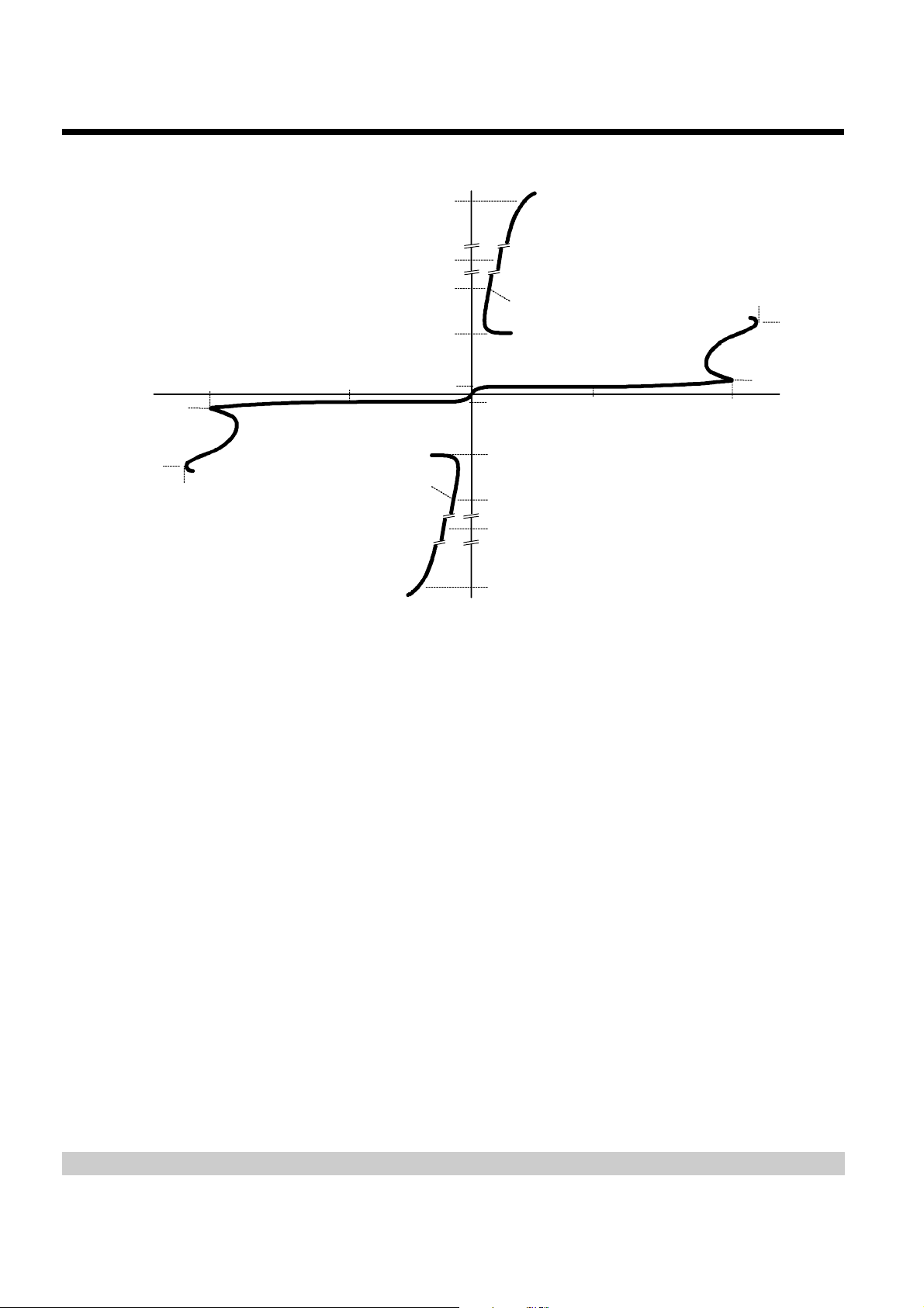
PARAMETER MEASUREMENT INFORMATION
-v
I
DRM
I
(BO)
V
Quadrant III
Switching
Characteristic
(BO)
+i
I
TSP
Characteristic
I
TSM
I
T
V
T
I
H
V
DRM
V
D
I
D
I
D
I
H
V
T
I
T
I
TSM
I
TSP
V
D
-i
Quadrant I
Switching
V
DRM
V
(BO)
I
DRM
PMXXAAB
I
(BO)
+v
Figure 1. VOLTAGE-CURRENT CHARACTERISTIC FOR T AND R TERMINALS
ALL MEASUREMENTS ARE REFERENCED TO THE R TERMINAL
PRODUCT INFORMATION
4
Page 5
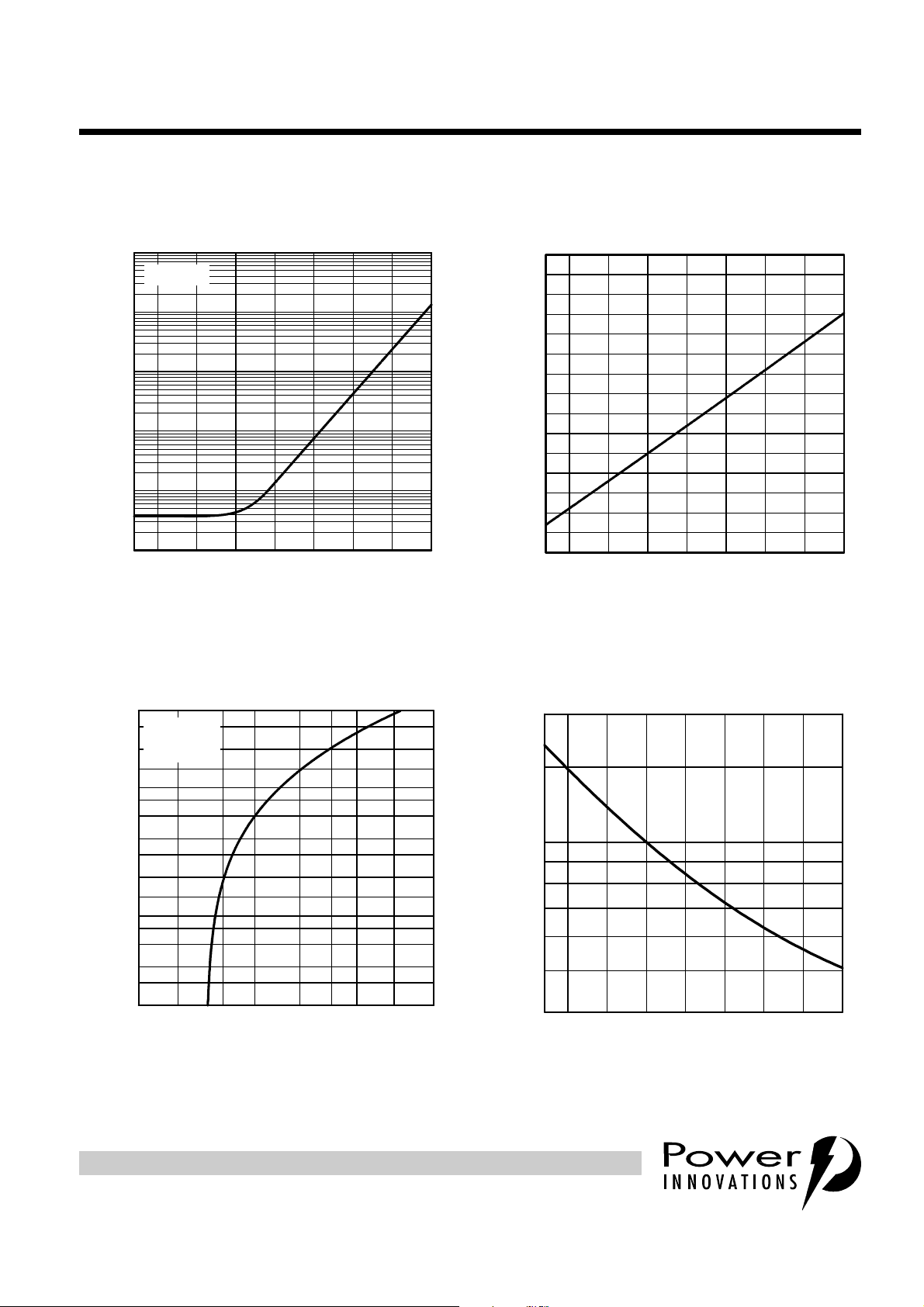
100
NORMALISED BREAKOVER VOLTAGE
vs
JUNCTION TEMPERATURE
TJ - Junction Temperature - °C
-25 0 25 50 75 100 125 150
Normalised Breakover Voltage
0.95
1.00
1.05
1.10
TC4HAF
NORMALISED HOLDING CURRENT
vs
JUNCTION TEMPERATURE
T
- Junction Temperature - °C
-25 0 25 50 75 100 125 150
Normalised Holdi ng Current
0.4
0.5
0.6
0.7
0.8
0.9
1.5
2.0
1.0
TC4HAD
10
0·1
| - Off-State Current - µA
D
|I
0·01
1
OFF-STATE CURRENT
vs
JUNCTION TEMPERATURE
VD = ±50 V
TISP4360H3BJ
BIDIRECTIONAL THYRISTOR OVERVOLTAGE PROTECTORS
JUNE 1999
TYPICAL CHARACTERISTICS
TCHAG
0·001
-25 0 25 50 75 100 125 150
TJ - Junction Temperature - °C
Figure 2. Figure 3.
ON-STATE CURRE NT
ON-STATE VOLTAGE
200
150
TA = 25 °C
100
- On-State Current - A
T
I
= 100 µs
t
W
70
50
40
30
20
15
10
7
5
4
3
2
1.5
1
0.7 1.5 2 3 4 5 7110
VT - On-State Voltage - V
Figure 4. Figure 5.
vs
TC4HACA
PRODUCT INFORMATION
5
Page 6

TISP4360H3BJ
BIDIRECTIONAL THYRISTOR OVERVOLTAGE PROTECTORS
JUNE 1999
TYPICAL CHARACTERISTICS
NORMALISED CAP ACI T ANCE
vs
OFF-STATE VOLTAGE
TJ = 25°C
= 1 Vrms
V
d
= 0
D
Capacitance Normalised to V
1
0.9
0.8
0.7
0.6
0.5
0.4
0.3
TC4HABA
0.2
0.5 1 2 3 5 10 20 30 50 100150
VD - Off-state Voltage - V
Figure 6.
PRODUCT INFORMATION
6
Page 7

BIDIRECTIONAL THYRISTOR OVERVOLTAGE PROTECTORS
MAXIMUM O VE RLOAD ON-STATE CURRENT
vs
CURRENT DURATION
t - Current Duration - s
0·01 0·1 1 10 100 1000
I - RMS Current - A
2
2.5
3
4
5
6
7
8
15
20
25
30
40
50
60
70
10
TI4HAJ
TISP4360H3BJ I
T(OV)M
V
GEN
= 600 Vrms, 50/60 Hz
R
GEN
= V
GEN
/I
T(OV)M
EIA/JESD51-2 ENVIRONMENT
EIA/JESD51-3 PCB
T
A
= 25 °C
UL 1950 600 V rms
TESTS (1, 2 & 5)
IMPULSE RATING
vs
AMBIENT TEMPERATURE
TA - Ambient Temperature - °C
-40-30-20-100 1020304050607080
Impulse Current - A
90
100
120
150
200
250
300
400
500
600
700
IEC 1.2/50, 8/20
ITU-T 10/700
FCC 10/560
BELLCORE 2/10
BELLCORE 10/1000
FCC 10/160
TC4HAA
RATING AND THERMAL INFORMATION
NON-REPETITIVE PEAK ON-STATE CURRENT
vs
30
20
15
10
CURRENT DURATION
V
= 600 Vrms, 50/60 Hz
GEN
R
= 1.4*V
GEN
EIA/JESD51-2 ENVIRONMENT
EIA/JESD51-3 PCB
T
= 25 °C
A
9
8
7
6
5
4
3
GEN
/I
TSM(t)
TI4HAC
TISP4360H3BJ
JUNE 1999
- Non-Repetiti ve Peak On-State Current - A
2
TSM(t)
I
1.5
0·1 1 10 100 1000
t - Current Duration - s
Figure 7. Figure 8.
V
DERATING FA CTOR
DRM
vs
MINIMUM AM BI ENT TEMPERAT U RE
1.00
0.99
0.98
0.97
PRODUCT INFORMATION
0.96
Derating Factor
0.95
0.94
0.93
-35 -25 -15 -5 5 15 25-40 -30 -20 -10 0 10 20
T
- Minimum Ambient Temperature - °C
AMIN
Figure 9. Figure 10.
TI4HADA
7
Page 8

TISP4360H3BJ
Th3
Th2
Th1
BIDIRECTIONAL THYRISTOR OVERVOLTAGE PROTECTORS
JUNE 1999
APPLICATIONS INFORMATION
deployment
These devices are two terminal overvoltage prote ctors. They may be used either singly to limit the voltage
between two conductors (Figure 11) or in multiples to limit the voltage at several points in a circuit (Figure 12).
Th1
Figure 11. TWO POINT PROTECTION Figure 12. MULTI-POINT PROTECTION
In Figure 11, protector Th1 limits the maximum voltage between the two conductors to ±V
configuration is nor mall y used to protect ci rcuits withou t a ground reference, such as modems. In Figure 1 2,
protectors Th2 and Th3 lim it the maximum voltage be tween each cond uctor and ground to the ±V
individual protector. Protector Th1 limits the maximum voltage between the two conductors to its ±V
value. If the equipment being protected has all its vulnerable components connected between the conductors
and ground, then protector Th1 is not required.
impulse testing
To verify the wit hstand capabil ity and safety of the equipment , standards require that the equipm ent is test ed
with various impulse wave forms. The table below shows some common values.
PEAK VOLTAGE
STANDARD
GR-1089-CORE
FCC Part 68
(March 1998)
I3124 1500 0.5/700 37.5 0.2/310 200 0
ITU-T K20/K21
† FCC Part 68 terminology for the waveforms produced by the ITU-T recommendation K21 10/700 impulse generator
SETTING
V
2500 2/10 500 2/10 500
1000 10/1000 100 10/1000 100
1500 10/160 200 10/160 250 0
800 10/560 100 10/560 160 0
1500 9/720 † 37.5 5/320 † 200 0
1000 9/720 † 25 5/320 † 200 0
1500
4000
VOLTAGE
WAVE FORM
µs
10/700
PEAK CURRENT
VALUE
A
37.5
100
CURRENT
WAVE FORM
µs
5/310 200 0
TISP4360H3BJ
25 °C RATING
A
SERIES
RESISTANCE
Ω
0
(BO)
(BO)
. This
of the
(BO)
Series resistance can be added to cover situations where ei ther the TISP4360H3BJ current rating will be
exceeded or excessive wiring currents result or both.
When a prim ary protector is used, the TISP4360 H3BJ may operate before the primar y protector. With the
TISP460H3BJ in a low voltage state, the pr imary prot ector is prevented from working. High curre nts, which
should have been carried by the primary protector, now flow through the wiring to the equipment and through
the TISP4360H3BJ. Interference and network equipm ent damage can occur, particul arly if the currents are
diverted to the l ocal ground. Protecto r co-ordination pr events this problem. A series resi stor can be used to
develop a voltage drop large enough to activate the pri mary protector. If the primary protector was a ga s
discharge tube (GDT) with a max imum d.c. sparkover of 400 V and the typical lightning impuls e decay time
was several hundred microseconds (TISP4360H3BJ ratin g 200 A) , a 2Ω series resistor ( 400 V/200 A) would
PRODUCT INFORMATION
8
Page 9

TISP4360H3BJ
BIDIRECTIONAL THYRISTOR OVERVOLTAGE PROTECTORS
be sufficient to achieve co-ordination. At peak currents of 200 A and above, the resistor would develop at least
400 V and GDT would switch and divert the current.
If the impulse generator current exceeds the protectors current rating then a series resistance can be used to
reduce the current to the protectors rate d value and so prevent possible failure. The required value of series
resistance for a given waveform is given by the following calculations. First, the minimum total circuit
impedance is found by dividing the impulse generators peak voltage by the protectors rated current. The
impulse generators fi ctive impedance (ge nerators peak voltage divided by peak shor t circu it current) is then
subtracted from the mini mum total circu it im pedance to give the req uired value of ser ie s res istance. In s ome
cases the equip ment will req uire verificatio n over a temperature range. By using the rated waveform values
from Figure 10, the appropriate series resistor value can be calculated for ambient temperatures in the range
of -40 °C to 85 °C.
a.c. testing
The protector can withstan d currents applied for times not exceeding thos e shown in Figure 7 . Currents tha t
exceed these times must be terminated or reduced to avoid protector failure. Fuses, PTC (Positive
Temperature Coefficient) resistors and fusible resistors are overcurrent protection devices which can be used
to reduce the current fl ow. Protective fuses may range from a few hundred milliamperes to o ne ampere. In
some cases it may be necessa ry to add some extra seri es resistance to prevent the fuse opening dur ing
impulse testing. The current versus time cha racteristic of the overcurrent protector must be below the line
shown in Figure 7. In some ca ses there may be a further time limit imposed by the test standard ( e.g. UL
1459/1950 wiring simulato r failure).
JUNE 1999
Safety tests require that the equipme nt fails without any hazard to th e user. For the equipment protector, this
condition usually means that the fault mode is short circuit, ensuring that the following circuitry is not exposed
to high voltages. The ratings table and Figure 8 detail the earliest times when a shorted condition could occur.
Figure 8 shows how the protector current levels compare to UL 1950 levels. Only the UL 1950 600 V tests (1,
2 and 3) are shown as these have sufficient voltage to operate the protector. Tests 4 (<285 V peak, 2.2 A) and
5 (120 V rms, 25 A) are too low in voltage to operate the protector.
Figure 8 shows that the TISP436 0H3BJ curve is very close o r better than the UL 1950 test levels. Design
compliance is si mply a m atte r of s elec tin g a n overcurrent pr ote cto r whi ch op erates b efore the UL 1 950 ti mes
up to 1.5 s. Fuses such as the Littelfuse 436 ser ies and 2AG (Surge Withstand type) se ries and Bussman n
TCP series have a 600 V capability for UL 1950. Fuses rated in the range of 0.5 A to 1.5 A will usually meet
the safety test requirements. However, the lower rated current value fuses may open on the type A surges of
FCC Part 68. Opening on a type A surge is not a test failure, but opening on a type B surge (37.5 A 5/320) is;
so the selected fuse must be able to withstand the type B surge.
capacitance
The protector characteristic off-state capacitance values are given for d.c. bias voltage, VD, values of 0, -1 V,
-2 V -50 V and -100 V. Values for other voltages may be calculated by multiplying the V
value by the factor given in Figure 6. Up to 10 MHz the capaci tance is essent ially indep endent of frequency.
Above 10 MHz the effective capacitance is strongly dependent on connection inductance.
= 0 capacitance
D
normal system voltage levels
The protector should not cl ip or limit the voltages that occur in norma l system operation. If the maximum
system voltages are not known, then de signers often used the voltages for the FCC Part 68 “B” rin ger. The
“B” ringer has a d.c. voltage of 56.5 and a maximum a.c. ring voltage of 150 V rms. The resultant waveform is
shown in Figure 13. The maxi mum voltage is -269 V, but, becaus e of possible wir ing reversals, the protector
should have a working voltage of ±269 V minimum. The standard TISP4350H3BJ protector meets this
requirement with a working voltage, V
shows the TISP4350H3BJ voltages relative to the POTS -269 V peak ringing voltage.
, of ±275 V and a protection voltage, V
DRM
, of ±350 V. Figure 14
(BO)
PRODUCT INFORMATION
9
Page 10

TISP4360H3BJ
BIDIRECTIONAL THYRISTOR OVERVOLTAGE PROTECTORS
JUNE 1999
200 V
100 V
0
-100 V
-200 V
-300 V
-56.5 V d.c.
+156 V
-269 V
AI4XAD
-230
-240
-250
-260
-270
-280
-290
-300
-310
-320
-330
-340
-350
-360
-370
-275 V
TISP4350H3BJ
-350 V
-269 V
RINGING PEAK
WORKING VOLTAGE V
PROTECTION VOLTAGE V
Figure 13. Figure 14.
The ADSL signal can b e as high as ±15 V and this adds to th e POTS signal making a peak value of -284 V.
This increased signal value of -284 V would be clipped by the TISP4350H3B J, which only all ows for a -275 V
signal. The TISP4360H3BJ has be en spe cified to overcome this pro blem by having a higher worki ng voltage
of ±290 V. Figure 15 shows the TISP4360H3BJ voltages relative to the -284 V peak ADSL plus POTS ringing
voltage. The ±15 V ADSL signal is shown as a grey band in Figure 15.
DRM
(BO)
AI4HAE
-230
-240
-250
-260
-270
-280
-290
-300
-310
-320
-330
-340
-350
-360
-370
-290 V
TISP4360H3BJ
-360 V
-284 V PEAK
ADSL + RINGING
WORKING VOLTAGE V
PROTECTION VOLTAGE V
DRM
(BO)
AI4HAF
Figure 15.
The recommended PC B pad layout for the TISP4360H3BJ SMB package (see mechanic al section) gives a
creepage distance o f 2.54 mm bet ween the device terminals. This distance value allows comp liance to the
minimum clearance values required by UL 1950 for operational, basic and supplementar y insulation and
creepage values for pollution degree 1.
PRODUCT INFORMATION
10
Page 11

TISP4360H3BJ
BIDIRECTIONAL THYRISTOR OVERVOLTAGE PROTECTORS
JESD51 thermal measurement method
To standardise thermal measurements, the EIA (Electronic Industries Alliance) has created the JESD51
standard. Part 2 of the standard (JESD51-2, 1995) describes the test environment. This is a 0.0283 m
cube which contains the test PCB (Printed Ci rcuit Board) horizontally mou nted at the centre. Part 3 of the
standard (JESD51-3, 199 6) defines two test PCB s for surface mount components; one for packages smaller
than 27 mm on a side and th e other for packages up to 48 mm. The SMBJ measureme nts used the sm aller
76.2 mm x 114.3 mm (3.0 “ x 4.5 “) PCB. The JESD51-3 PCBs are design ed to have low effective thermal
conductivity (high th er mal resi stance) and represen t a worse case con dition . The PCBs us ed in the ma jority
of applications will a chieve lower values of thermal resis tance and s o can dis sipate higher power levels than
indicated by the JESD51 values.
JUNE 1999
3
(1 ft3)
PRODUCT INFORMATION
11
Page 12

TISP4360H3BJ
BIDIRECTIONAL THYRISTOR OVERVOLTAGE PROTECTORS
JUNE 1999
typical circuits
RING
TIP
FUSE
TISP4360
MODEM
RING DETECTOR
HOOK SWITCH
D.C. SINK
SIGNAL
AI6XBMB
TIP
WIRE
RING
WIRE
R1a
Th1
R1b
Th3
Th2
PROTECTED
EQUIPMENT
E.G. LINE CARD
Figure 16. MODEM INTER-WIRE PROTECTION Figure 17. PROTECTION MODULE
R1a
Th3
Th1
Th2
R1b
D.C.
SIGNAL
AI6XBL
Figure 18. ISDN PROTECTION
AI6XBK
TIP
WIRE
RING
WIRE
OVER-
CURRENT
PROTECTION
R1a
R1b
RING/TEST
PROTECTION
Th3
Th1
Th2
TEST
RELAY
S1a
S1b
TEST
EQUIP-
MENT
RING
RELAY
S2a
S2b
RING
GENERATOR
Figure 19. LINE CARD RING/TEST PROTECTION
SLIC
RELAY
S3a
S3b
SLIC
PROTECTION
Th4
Th5
TISP6xxxx,
TISPPBLx,
½TISP6NTP2
C1
220 nF
SLIC
V
BAT
AI6XBJ
PRODUCT INFORMATION
12
Page 13

TISP4360H3BJ
BIDIRECTIONAL THYRISTOR OVERVOLTAGE PROTECTORS
MECHANICAL DATA
SMBJ (DO-214AA)
plastic surface mount diode package
This surface mount package consist s of a circ uit moun ted on a lea d frame and en caps ulated within a pl astic
compound. The compound will withstand soldering temperature with no deformation, and circuit performance
characteristics will remain stable when operated in high humidity conditions. Leads require no additional
cleaning or processing when used in soldered assembly.
SMB
4,57
4,06
JUNE 1999
3,94
3,30
2,40
2,00
1,52
0,76
Index
Mark
(if needed)
2,10
1,90
5,59
5,21
2
0,20
0,10
2,32
1,96
ALL LINEAR DIMENSIONS IN MILLIMETERS
PRODUCT INFORMATION
MDXXBHA
13
Page 14

TISP4360H3BJ
BIDIRECTIONAL THYRISTOR OVERVOLTAGE PROTECTORS
JUNE 1999
MECHANICAL DATA
recommended printed wiring footprint.
SMB Pad Size
2.54
2.40
2.16
ALL LINEAR DIMENSIONS IN MILLIMETERS
MDXXBI
device symbolization code
Devices will be coded as below. As the device parameters are symmetrical, terminal 1 is not identified.
DEVICE
TISP4360H3BJ 4360H3
SYMOBLIZATION
CODE
carrier info r m a tion
Devices are shipped in on e of the carriers be low. Unless a specific method of shipment is s pecified by the
customer, devices will be shipped in the most practical carrier. For production quantities the carr ier will be
embossed tape reel pack. Evaluation quantities may be shipped in bulk pack or embossed tape.
CARRIER ORDER #
Embossed Tape Reel Pack TISP4360H3BJR
Bulk Pack TISP4360H3BJ
PRODUCT INFORMATION
14
Page 15

tape dimensions
SMB Package Single-Sprocket Tape
TISP4360H3BJ
BIDIRECTIONAL THYRISTOR OVERVOLTAGE PROTECTORS
JUNE 1999
MECHANICAL DATA
8,10
7,90
Direction of Feed
4,10
3,90
2,05
1,95
ø 1,5 MIN.
Carrier Tape
Embossment
Index
Mark
(if needed)
1,65
1,55
20°
1,85
1,65
5,55
5,45
0 MIN.
Maximium com ponent
rotation
Typical compon ent
cavity centre line
Typical compon ent
centre line
12,30
11,70
Cover
Tape
0,40 MAX.
8,20
MAX.
4,5 MAX.
ALL LINEAR DIMENSIONS IN MILLIMETERS
NOTES: A. The clearance between the component and the cavity must be within 0,05 mm MIN. to 0,65 mm MAX. so that the
component cannot rotate more than 20° within the determined cavity.
B. Taped devices are supplied on a reel of the following dimensions:-
Reel diam et e r: 330 ±3,0 mm
Reel hub diameter 75 mm MIN.
Reel axial hole: 13,0 ±0,5 mm
C. 3000 devices are on a reel.
PRODUCT INFORMATION
MDXXBJ
15
Page 16

TISP4360H3BJ
BIDIRECTIONAL THYRISTOR OVERVOLTAGE PROTECTORS
JUNE 1999
IMPORTANT NOTICE
Power Innovations Limited (PI) re se rves the r ig ht t o make chan g es t o it s pr od uc ts o r t o di sc ont inu e any s em ic o nduc t or p r o duct
or service without notice, and advises its customers to verify, before placing orders, that the information being relied on is
current.
PI warrants performance of its semiconductor products to the specifications applicable at the time of sale in accordance with
PI's standard w arr anty. Testing and other quality cont rol tec hn iqu es are uti li z ed to the exten t PI deems necessary to support this
warranty. Specific testing of all parameters of each device is not necessarily performed, except those mandated by government
requirements.
PI assumes no liability for applications assistance, customer product design, software performance, or infringement of patents
or services described herein. Nor is any license, either express or implied, granted under any patent right, copyright, design
right, or other intellectual property right of PI covering or relating to any combination, machine, or process in which such
semiconductor products or services might be or are used.
PI SEMICONDUCTOR PRODUCTS ARE NOT DESIGNED, INTENDED, AUTHORISED, OR WARRANTED TO BE SUITABLE
FOR USE IN LIFE-SUPPORT APPLICATIONS, DEVICES OR SYSTEMS.
Copyright © 1999, Power Innovations Limited
PRODUCT INFORMATION
16
 Loading...