

Page 1
BIDIRECTIONAL THYRISTOR OVERVOLTAGE PROTECTORS
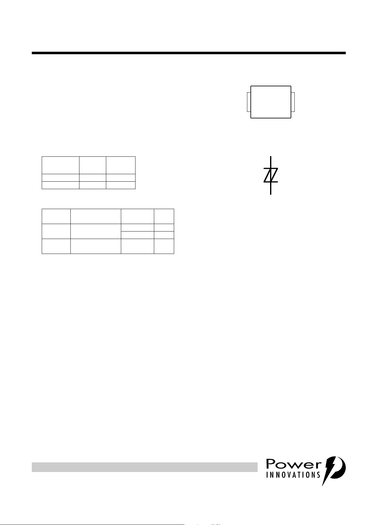
device symbol
FCC PART 68 AND UL 1950 OVERVOLTAGE PROTECTORS
●
MODEM Protection against:
— FCC Part 68 Type A & B surge
— UL 1950, Clause 6. powe r cross
— CSA 22.2 No. 950, Clause 6. power cross
●
Ring-Tip Protection...............TISP4350L3BJ
●
Electronics Protection ..........TISP4070L3BJ
●
Ion-Implanted Breakdown Region
Precise and Stable Voltage
Low Voltage Overshoot under Surge
V
DEVICE
‘4070 58 70
‘4350 275 350
●
Rated for UL 1950 and Part 68 Wave Shapes
SURGE
TYPE
A FCC Part 68
B
DRM
V
STANDARD
FCC Part 68
UL 1950 / ITU-T K21
V
(BO)
V
WAVE
SHAPE
10/160 µs 50
10/560 µs 30
9/720 µs
10/700 µs
I
TSP
40
TISP4070L3BJ, TISP4350L3BJ
AUGUST 1999 — REVISED NOVEMBER 1999Copyright © 1999, Power Innovations Limited, UK
SMBJ PACKAGE
(TOP VIEW)
12
T
R
erminals T and R cor respond to the
T
A
alternative line designators of A and B
T(A)R(B)
MDXXBG
SD4XAA
description
These devices are designed to limit overvoltages on the telephone line. Overvoltages are normally caused by
a.c. power system or lightning flash disturbances whic h ar e ind uc ed or co ndu cte d on to the telephone li ne. A
single device provides 2-point protection and is typically u sed for the protec tion of 2 -wire tel ecommunicatio n
equipment (e.g. between the Ri ng and Tip wires for telephones a nd modems ). Combinati ons of devices ca n
be used for multi-point protection (e.g. 3-point protection between Ring, Tip and Ground).
The protector consists of a symmetrical voltage-triggered bidirectional thyristor. Overvoltages are initially
clipped by breakdown clamping until the voltage rises to the breakover level, which causes the device to
crowbar into a low-voltage on state. This low-voltage on state causes the current resulting from the
overvoltage to be safely diverted through the device. The high crowbar holding cu rrent prevents d.c. latchup
as the diverted c urrent subsides.These protectors are guaranteed t o voltage limit and wi thstand the listed
lightning surges in both polarities.
After a Type A surge the equipment can be faulty, provided that the fault mode causes the equ ipment to be
unusable. The high current Type A surges (10/160, 200 A an d 10/560, 100 A), will cause the TISP 4xxxL3 BJ
to fail short circuit, giving a non-operational equipment pass to Type A surges.
After a Type B surge the equi pment must be operational . As the TISP4x xxL3 BJ h as a c urrent rating o f 40 A,
will survive both Type B surges, metallic (differential mode 25 A, 9/720) and longitudinal (common mode
37.5 A, 9/720), giving an operational pass to Type B surges.
For metallic protection, the TISP4350L3BJ is connected between the Ring and Tip conductors. For
longitudinal protection two TISP43 50L3BJ protectors are used; one between the Rin g conductor to ground
and the other between the Tip conduc tor to ground. The B type r inger has voltages of 56. 5 V d.c. and up to
PRODUCT INFORMATION
Information is current as of publication date. Produc ts conform to specifications in accordance
with the terms of Power Innovations standard warranty. Production processing does not
necessarily include testing of all parameters.
1
Page 2

TISP4070L3BJ, TISP4350L3BJ
BIDIRECTIONAL THYRISTOR OVERVOLTAGE PROTECTORS
AUGUST 1999 — REVISED NOVEMBER 1999
150 V rms a.c., giving a peak voltage of 269 V. The TISP4350L3BJ will not clip the B type ringing voltage as it
has a high impedance up to 275 V.
The TISP4070L3BJ should be connected after the hook switch to protect the following electronics. As the
TISP4070L3BJ has a high imp edance up to 58 V, it will switch off after a surge and not be triggered by the
normal exchange battery voltage
These low (L) current protection devices are in a plastic package SMBJ (JEDEC DO-214AA with J-bend
leads) and supplied in embossed tape reel pack. For alternative voltage and holding current values, consu lt
the factory. For higher rated impuls e curr ents i n the S MB package, the 100 A 10/1000 TI SP4xxx H3BJ ser ies
is available.
T
absolute maximum ratings,
Repetitive peak off-state voltage,
Non-repetitive peak on-state pulse current (see Notes 1, and 2)
10/160 µs (FCC Part 68, 10/160 µs voltage wave shape, Type A) 50
5/310 µs (ITU-T K21, 10/700 µs voltage wave shape) 40
5/320 µs (FCC Part 68, 9/720 µs voltage wave shape, Type B) 40
10/560 µs (FCC Part 68, 10/560 µs voltage wave shape, Type A) 30
Non-repetitive peak on-state current (see Notes 1, 2 and 3)
20 ms (50 Hz) full sine wave
16.7 ms (60 Hz) full sine wave
1000 s 50 Hz/60 Hz a.c.
Initial rate of rise of on-state current, Exponential current ramp, Maximum ramp value < 100 A di
Junction temperature T
Storage temperature range T
= 25 °C (unless otherwise noted)
A
RATING SYMBOL VALUE UNIT
‘4070
‘4350
V
DRM
I
TSP
I
TSM
/dt 120 A/µs
T
J
stg
± 58
±275
12
13
2
-40 to +150 °C
-65 to +150 °C
V
A
A
NOTES: 1. Initially the TISP4xxxL3BJ must be in thermal equilibrium with T
2. The surge may be repeated after the TISP4xxxL3BJ returns to its initial conditions.
3. EIA/JESD51-2 environment and EIA/JESD51-3 PCB with standard footprint dimensions connected with 5 A rated printed wiring
track widths. Derate current values at -0.61 %/°C for ambient temperatures above 25°C
T
overload ratings,
Peak ov erload on-state current, Type A impulse (see Note 4)
10/160 µs
10/560 µs
Peak overload on-state current, a.c. power cross tests UL 1950 (see Note 4) I
NOTE 4: These electrical stress levels may damage the TIS4xxxL3BJ silicon chip. After test, the pass criterion is either that the device is
functional or, if it is faulty, that it has a short circuit fault mode. In the short circuit fault mode, the following equipment is protected
as the device is a permanent short across the line. The equipment would be unprotected if an open circuit fault mode developed.
= 25 °C (unless otherwise noted)
A
RATING SYMBOL VALUE UNIT
=25°C.
J
I
T(OV)M
T(OV)M
300
150
See Figure 2
for cu rrent
versus time
A
A
PRODUCT INFORMATION
2
Page 3
TISP4070L3BJ, TISP4350L3BJ
BIDIRECTIONAL THYRISTOR OVERVOLTAGE PROTECTORS
AUGUST 1999 — REVISED NOVEMBER 1999
electrical characterist ics for the T and R terminals, TA = 25 °C (unless otherwise noted)
PARAMETER TEST CONDITIONS MIN TYP MAX UNIT
I
DRM
V
(BO)
V
(BO)
I
(BO)
V
T
I
H
dv/dt
I
D
C
off
Repetitive peak offstate current
Breakover voltage dv/dt = ±250 V/ms , R
= V
V
D
DRM
Ω
= 300
SOURCE
dv/dt≤±1000 V/µs, Linear voltage ramp,
Impulse breakover
voltage
Maximum ramp value = ±500 V
di/dt = ±20 A/µs, Linear current ramp,
Maximum ramp value = ±10 A
Breakover current dv/dt = ±250 V/ms, R
SOURCE
= 300
Ω
On-state voltage IT=±5A, tW= 100 µs ±3 V
Holding current IT= ±5 A, di/dt = +/-30mA/ms ±120 ±350 mA
Critical rate of rise of
off-state voltage
Linear voltage ramp, Maximum ramp value < 0.85V
Off-state current VD=±50V TA = 85 °C ±10 µA
Off-state capacitance
f = 100 kHz , V
f = 100 kHz, V
=1V rms, VD=0
d
V
D
V
D
=1V rms, VD=0
d
V
D
V
D
=1V
=5V
=1V
=5V
DRM
TA = 25 °C
= 85 °C
T
A
‘4070
‘4350
‘4070
‘4350
‘4070
‘4350
±40 ±250 mA
±5 kV/µs
40
38
31
26
24
20
±5
±10
±70
±350
±78
±359
50
48
39
33
30
25
µA
V
V
pF
thermal characteristics
PARAMETER
EIA/JESD51-3 PCB, I
T
= 25 °C, (see Note 5)
R
Junction to free air thermal resistance
θ
JA
A
265 mm x 210 mm populated line card,
4-layer PCB, I
TEST CONDITIONS
= I
T
TSM(1000)
= I
T
TSM(1000)
, TA = 25 °C
,
NOTE 5: EIA/JESD51-2 environment and PCB has standard footprint dimensions connected with 5 A rated printed wiring track widths.
MIN TYP MAX UNIT
115
°C/W
52
PRODUCT INFORMATION
3
Page 4
TISP4070L3BJ, TISP4350L3BJ
BIDIRECTIONAL THYRISTOR OVERVOLTAGE PROTECTORS
AUGUST 1999 — REVISED NOVEMBER 1999
PARAMETER MEASUREMENT INFORMATION
-v
I
DRM
I
(BO)
V
Quadrant III
Switching
Characteristic
(BO)
+i
I
TSP
Characteristic
I
TSM
I
T
V
T
I
H
V
DRM
V
D
I
D
I
D
I
H
V
T
I
T
I
TSM
I
TSP
V
D
-i
Quadrant I
Switching
V
DRM
V
(BO)
I
DRM
PMXXAAB
I
(BO)
+v
Figure 1. VOLTAGE-CURRENT CHARACTERISTIC FOR T AND R TERMINALS
ALL MEASUREMENTS ARE REFERENCED TO THE R TERMINAL
PRODUCT INFORMATION
4
Page 5
BIDIRECTIONAL THYRISTOR OVERVOLTAGE PROTECTORS
THERMAL INFORMATION
PEAK OVERLOAD O N-STATE CURRENT
vs
40
35
30
25
40 A
20
15
10
9
8
7
6
5
4
3.5
3
— Peak Overload On-State Current — A rms
2.5
T(OV)M
I
2
0·01 0·1 1 10 100 1000
CURRENT DURATION
TISP4xxxL3BJ WILL
CARRY CURRENT
100 A2s
WIRING
SIMULATOR
t - Current Duration - s
OF TESTS 1 THRU 5
CLAUSE 6.6, UL 1950,
FOR FULL TEST TIME
7 A
TISP4070L3BJ, TISP4350L3BJ
AUGUST 1999 — REVISED NOVEMBER 1999
TI4LAA
2.2 A
Figure 2. PEAK OVERLOAD ON-STATE CURRENT AGAINST DURATION
APPLICATIONS INFORMATION
UL 1950, CSA C22.2 No. 950 and EN 60950
These electrical safety standar ds for IT (Informatio n Technology) equipment at the cus to mer pr em is e use the
IEC (International Electro-technical Commission) 60950 standard as the core document. The IEC 60950
covers fundamental safety criter ia such as creepage an d isolation. The connec tion to a telecommunicatio n
network voltage (TNV) is covered in clause 6.
Europe is harmonised by CENELEC (Comité Européen de Normalization Electro-technique) under EN 60950
(included in the L ow Voltage Directive, CE mark). US has UL (Underwr iters Laborator ies) 1 950 and Ca nada
CSA (Canadian Standards Authority) C22.2 No. 950. The US and Canadian standards include regional
changes and additions to the IEC 60950. A major addition is the inclusion of clause 6.6, power cross
withstand and ann ex NAC covering t esting. Remar ks made for UL 1950 will generally be true for CSA 22.2
No. 950.
UL 1950, clause 6.6 — power cross
Figure 3 shows the cr iterion flow for UL 1950 power cross. (This is a modified version of UL1950 , Figure
18b — Overvoltage flowchart) There are many routes for achieving a pass result. For discussion, each
criterion has been given a letter reference. Brief details of any electr ical testing is given as a cr iterion note.
Test pass criteria are given in the bottom table of Figure 3.
PRODUCT INFORMATION
5
Page 6

TISP4070L3BJ, TISP4350L3BJ
BIDIRECTIONAL THYRISTOR OVERVOLTAGE PROTECTORS
AUGUST 1999 — REVISED NOVEMBER 1999
IT Equipment
parame ters
Connects
to outs ide
cable
Yes
Has
≤
100 A2s
@ 600 V
† )
Yes
Has
≤
1.3 A
d.c.
limiting ‡ )
Yes
UL 1950 Third Edition
Telecommunication network connection
Clause 6 .6 — P rotection a gain st overvo ltage from p ow e r line crosses
Figu re 18b — Overvoltage flow ch art
Annex NAC (normative) — Power line crosses
A
No
Test 1.
600 V, 40 A,
1.5 s
B
No
C
Test 2.
¶ )
600 V, 7 A, 5 s
Test 3.
# )
600 V, 2.2 A,
30 min or open circuit (3A)
Test 3A. # )
600 V, < 2.2 A, 30 min, no
open circuit
# )
Test 4.
< Limiting voltage, < 2.2 A,
30 min, no open circuit, no
overvoltage protector
voltage limiting
Has min.
26 AWG
supplied
cord
Yes
Pass 6.3.3
ground/line
separation
§ )
Yes
Has fire
enclosure
and
spacings
No
E
No
Pass Test 1
Yes
F
NoNo
Pass test 5
Yes
I
Test 5
120 V, 25 A,
30 min or
open circuit
J
No
G
No
No overvoltage
testing
No
.
Fail
Yes
Has
fire
enclos u r e
NOTES
† )
Overcurrent protector I2t must must be lower than any other equipment element which carries the same current.
‡ )
UL accepts that a fuse with a 1 A or less rating meets the 1.3 A criterion.
§ )
Pass for 1 20 V a.c. bet ween telecommunication line a nd ground cur rent < 10 mA.
Test 2 not required if the equipment d.c. breaking is 1.3 A or less, see comment ‡ ).
¶ )
# )
Tests 3 and 4 not requ ir e d for equipment with less t h an 1000 m of ou tside cable.
Pass c r ite ria
No cheesecloth charring
Insu la t io n O K
wirin g s imula to r (f u se ) OK
August 1999 V2.3
I
D
No
2
t < 100 A2s @ 600 V a.c.
Test 1
✔
✔
✔
✔
Pass test 2
pass tests
Figure 3. UL 1950 POWER CROSS FLOW CHART
PRODUCT INFORMATION
6
3, 4
Yes
Test 2
✔
✔
H
Test 3
✔
✔
Yes
Test 3A
✔
✔
Test 4
✔
✔
Test 5
✔
✔
✔
Pass
Users must verify
requirements against
latest issue of UL 1950
Page 7

power cross pass routes
This discussion covers typical modem flo ws.
FLOW COMMENT
A
N
Y
No tests
B
A
Y
N
B
Y
E
C
TISP4070L3BJ, TISP4350L3BJ
BIDIRECTIONAL THYRISTOR OVERVOLTAGE PROTECTORS
AUGUST 1999 — REVISED NOVEMBER 1999
box A
The criter ion for box A is if the m odem connects to an outside TNV
line.
The majority of modems will be connected to an outside line, so the
answer is
yes
box B
The criter ion for box B is if the equipmen t has a limit of ≤ 100 A2s at
600 V rms for Te st 1. Many interpret this as a fuse with I
and often miss the 600 V a.c. breaking requirement. However, the
current loop is completed by the fuse and other equipment
components. To ensure that the fuse I
performance, the other current loop components, such as t he printed
wiring (PW), must have a higher I
2
fuse I
example IC packaging, may impose a hazard-free limit of 10 A
conflicts with FCC Part 68 Type A surge pass requirement of 8 A
t needs to be lower than 100 A2s but other components, for
. The
yes
path goes to box B.
2
2
t≤100 A2s
2
t sets the equipment
t values than the fuse. Certainly t he
2
s. (This
2
s.)
N N
E
Y Y
F
yes
leads to box C and a no to box E.
A
boxes E and I
I
Fail
The criterion for box E is for a minimum telecommunications line cord
of No. 26 AWG to be supplied or specified.
yes
leads to box F and a no to box I.
A
The criterion for box I is to pass Test 1.
yes
If all the four pass criter ia of Test 1 are met, this is a
and the flow
goes to box F.
no
result fails the equipment.
A
PRODUCT INFORMATION
7
Page 8

TISP4070L3BJ, TISP4350L3BJ
BIDIRECTIONAL THYRISTOR OVERVOLTAGE PROTECTORS
AUGUST 1999 — REVISED NOVEMBER 1999
FLOW COMMENT
boxes C and D
A
B
C
Y
Y
N
Y
F
The criterion for box C is overcurrent protection that reduces cu rrents
above 1.3 A. This requirement is met by a 1 A fuse (a 1 A current
fusing rating, not an IEC 1 A current carrying rating).
Modems which pass FCC Part 68 Type B surges and nonoperationally pass Type A surge s ca n us e a fu se of 1 A or less, so the
yes
path to box D can be followed. High performan ce modems which
operationally pass both Type A and B surges would need a fuse of
greater than 1 A and so follow the
no
path to box F.
D
N
Y
H
Pass
The criterion for box D is a fire enclosure.
Few modems can afford fire enclosures. However, for an internal
modem in a known comput er case, the case may be evaluated as a
yes
fire enclosure. A successful case evaluation will give a
equipment pass.
More likely the modem will not have a fire enclosure. The
to box H.
and an
no
flow goes
boxes F and J
F
G
N
Y
N
J
Y
Fail
The criterion for box F is a pass to clause 6.3.3 requirements.
yes
A
goes to box G and a no goes to box J.
The criterion for box J is to pass Test 5.
If all the three pass cr i teria of Test 5 are met, this is a
goes to box G.
no
A
result fails the equipment.
yes
and the flow
PRODUCT INFORMATION
8
Page 9

BIDIRECTIONAL THYRISTOR OVERVOLTAGE PROTECTORS
FLOW COMMENT
boxes G and H
The criteri on for box G is a fire enclos ure and spacings (See box D
comments).
yes
result passes the equipment and a no result leads to box H.
A
G
Fail
Y
N
TISP4070L3BJ, TISP4350L3BJ
AUGUST 1999 — REVISED NOVEMBER 1999
H
Y
N
Pass
The criterion for box H is to pass Tests 2, 3 and 4. Test 2 is not required
if there is overcurrent protection that reduces currents above 1.3 A
(See box C).
High performance modem s, using fuses and without fire enclosures,
must pass tests 2, 3, possibly 3A if the fuse opens, and 4. For standard
modems, using fuses o f 1 A or less and without fire encl osures, tests
3, 3A and 4 must be passed.
If the two pass criteria of each of the tests performed are met, this is a
yes
and the equipment passes.
no
result fails the equipment.
A
fuse values
There are two areas of fuse criteria; surge capability (FCC Part 68 impulse) and power cross capability
(UL1950 clause 6.6 and annex NAC).
2
To s ur vive an impuls e, a fuse mus t have a melting I
should be specified for the impuls e waveshape current as the normal d.c. rating may not result in adiabatic
conditions. Alternatively, the fuse may be specified for a rated current under the impulse waveshape
conditions.
An exponentially decaying imp ulse with a cu rren t amp litude I
2
I
t value of 0.72I
2
tD. Test wavef orms have tolerences and the formula can be approximated to I
PP
about an 40 % allowance to cover tolerences e.g. +5 % on I
formula, the I
2
t values for typical waveforms are shown in the table below.
t rating greater than the impulse I2t. The fuse I2t rating
and 50 % amplitude decay time of tD has an
PP
and +30 % on tD. Using the approximate
PP
2
tD, giving
PP
SPECIFICATION
FCC Part 68, Type A
FCC Part 68, Type B 37.5 5/320 0.45
UL 1950 / ITU-T K21 37.5 5/310 0.45
TELCORDIA (FORMALLY BELLCORE)
GR-1089
AMPLITUDE I
A
200 10/160 6.4
100 10/560 5.6
500 2/10 2.5
100 10/1000 10
CURRENT WAVESHAPE
PP
tR/tD (µs)
MELTING I
2
t
2
s
A
Fuse power cross current capability can be determined from it’s time-current curve. The fuse must be rated to
break the current at the applied power cross a.c. voltage level.
fuse values for FCC Part 68
Fuses must not blow on the Type B surge. To s urvive a 37.5 A Type B surge, the fuse needs t o have an I2t of
greater than 0.45 A
lead 2AG Surge Withstand 230.500 (both from the Littelfuse) will meet this criteria.
2
s. Fuses, such as the 1 A surface mount SMTe lecom™ 0436001 .PR or the 0.5 A axial
PRODUCT INFORMATION
9
Page 10

TISP4070L3BJ, TISP4350L3BJ
BIDIRECTIONAL THYRISTOR OVERVOLTAGE PROTECTORS
AUGUST 1999 — REVISED NOVEMBER 1999
To survive the Ty pe A surg es a fus e I2t value of 6.4 A2s is needed. Fuses, such as the 1.6 A 043601.6PR will
meet this criteria.
fuse values for UL 1950
Fuses for the UL 1950 power cross need to break the specified currents at 600 V a.c. - ordinary fuses will not
do! Fuse specification terms like
600 V a.c.
The requirement of Figure 3, box B, limits the fuse I
Box C, with its 1.3 A limit gives a flow division. Mod ems passing the FCC Part 68 Type A surge in a non-
operational mode, could u se a 1 A fuse and sati sfy the 1.3 A limit and move to box D. Modems operationally
passing the Type A surge will tend to use a 1.6 A fuse a fuse and move to box F. Fuses with ratings of 2 A and
above may not operate before the wiring simulator fails.
ensure that the 600 V breaking is met.
TISP4xxxL3BJ and UL 1950 power cross
The TISP4xxxL3BJ conduct s current for periods greater than the power cross test times, Figure 2, so the
TISP4xxxL3BJ is not a major factor in UL 1950 c ompliance. The ma in design task for UL 1950 power cros s
is about enclosure design and the selection of the other compo nents that are subject to power cross. A UL
specified fuse togethe r with a TISP4xxxL3BJ gives a simple design approach to mee ting the power cross
requirements.
short ci rcuit capabilities to UL 1459 and UL 1950 , 40 A, 7 A and 2.2 A at
2
t to less than 100 A2s.
PRODUCT INFORMATION
10
Page 11

TISP4070L3BJ, TISP4350L3BJ
BIDIRECTIONAL THYRISTOR OVERVOLTAGE PROTECTORS
AUGUST 1999 — REVISED NOVEMBER 1999
MECHANICAL DATA
SMBJ (DO-214AA)
plastic surface mount diode package
This surface mount package consist s of a circ uit moun ted on a lea d frame and en caps ulated within a pl astic
compound. The compound will withstand soldering temperature with no deformation, and circuit performance
characteristics will remain stable when operated in high humidity conditions. Leads require no additional
cleaning or processing when used in soldered assembly.
SMB
4,57
4,06
3,94
3,30
2,40
2,00
1,52
0,76
Index
Mark
(if needed)
2,10
1,90
5,59
5,21
2
0,20
0,10
2,32
1,96
ALL LINEAR DIMENSIONS IN MILLIMETERS
PRODUCT INFORMATION
MDXXBHA
11
Page 12

TISP4070L3BJ, TISP4350L3BJ
BIDIRECTIONAL THYRISTOR OVERVOLTAGE PROTECTORS
AUGUST 1999 — REVISED NOVEMBER 1999
MECHANICAL DATA
recommended printed wiring footprint.
SMB Pad Size
2.54
2.40
2.16
ALL LINEAR DIMENSIONS IN MILLIMETERS
MDXXBI
device symbolization code
Devices will be coded as below. As the device parameters are symmetrical, terminal 1 is not identified.
PRODUCTION
DEVICE
TISP4070L3BJ 4070L3 TX4070
TISP4350L3BJ 4350L3 TX4350
SYMBOLIZATION
CODE
DEVELOPMENT
SYMBOLIZATION
CODE
carrier info r m a tion
Devices are shipped in on e of the carriers be low. Unless a specific method of shipment is s pecified by the
customer, devices will be shipped in the most practical carrier. For production quantities the carr ier will be
embossed tape reel pack. Evaluation quantities may be shipped in bulk pack or embossed tape.
AVAILABLE OPTIONS
PACKAGE TYPE
SMBJ (DO-214AA) TISP4xxxL3BJ TISP4xxxL3BJR
BULK PACK TAPE AND REEL
CARRIER
PRODUCT INFORMATION
12
Page 13

tape dimensions
SMB Package Single-Sprocket Tape
TISP4070L3BJ, TISP4350L3BJ
BIDIRECTIONAL THYRISTOR OVERVOLTAGE PROTECTORS
AUGUST 1999 — REVISED NOVEMBER 1999
MECHANICAL DATA
8,10
7,90
Direction of Feed
4,10
3,90
2,05
1,95
ø 1,5 MIN.
Carrier Tape
Embossment
Index
Mark
(if needed)
1,65
1,55
20°
1,85
1,65
5,55
5,45
0 MIN.
Maximium com ponent
rotation
Typical compon ent
cavity centre line
Typical compon ent
centre line
12,30
11,70
Cover
Tape
0,40 MAX.
8,20
MAX.
4,5 MAX.
ALL LINEAR DIMENSIONS IN MILLIMETERS
NOTES: A. The clearance between the component and the cavity must be within 0,05 mm MIN. to 0,65 mm MAX. so that the
component cannot rotate more than 20° within the determined cavity.
B. Taped devices are supplied on a reel of the following dimensions:-
Reel diam et e r: 330 ±3,0 mm
Reel hub diameter 75 mm MIN.
Reel axial hole: 13,0 ±0,5 mm
C.
3000 devices are on a reel.
PRODUCT INFORMATION
MDXXBJ
13
Page 14

TISP4070L3BJ, TISP4350L3BJ
BIDIRECTIONAL THYRISTOR OVERVOLTAGE PROTECTORS
AUGUST 1999 — REVISED NOVEMBER 1999
IMPORTANT NOTICE
Power Innovations Limited (PI) re se rves the r ig ht t o make chan g es t o it s pr od uc ts o r t o di sc ont inu e any s em ic o nduc t or p r o duct
or service without notice, and advises its customers to verify, before placing orders, that the information being relied on is
current.
PI warrants performance of its semiconductor products to the specifications applicable at the time of sale in accordance with
PI's standard w arr anty. Testing and other quality cont rol tec hn iqu es are uti li z ed to the exten t PI deems necessary to support this
warranty. Specific testing of all parameters of each device is not necessarily performed, except those mandated by government
requirements.
PI assumes no liability for applications assistance, customer product design, software performance, or infringement of patents
or services described herein. Nor is any license, either express or implied, granted under any patent right, copyright, design
right, or other intellectual property right of PI covering or relating to any combination, machine, or process in which such
semiconductor products or services might be or are used.
PI SEMICONDUCTOR PRODUCTS ARE NOT DESIGNED, INTENDED, AUTHORISED, OR WARRANTED TO BE SUITABLE
FOR USE IN LIFE-SUPPORT APPLICATIONS, DEVICES OR SYSTEMS.
Copyright © 1999, Power Innovations Limited
PRODUCT INFORMATION
14
 Loading...