

Datasheet TISP4265H4BJ, TISP4360H4BJ, TISP4300H4BJ, TISP4165H4BJ, TISP4200H4BJ Datasheet (Power Innovations)
...Page 1
TISP4165H4BJ THRU TISP4200H4BJ, TISP4265H4BJ THRU TISP4360H4BJ
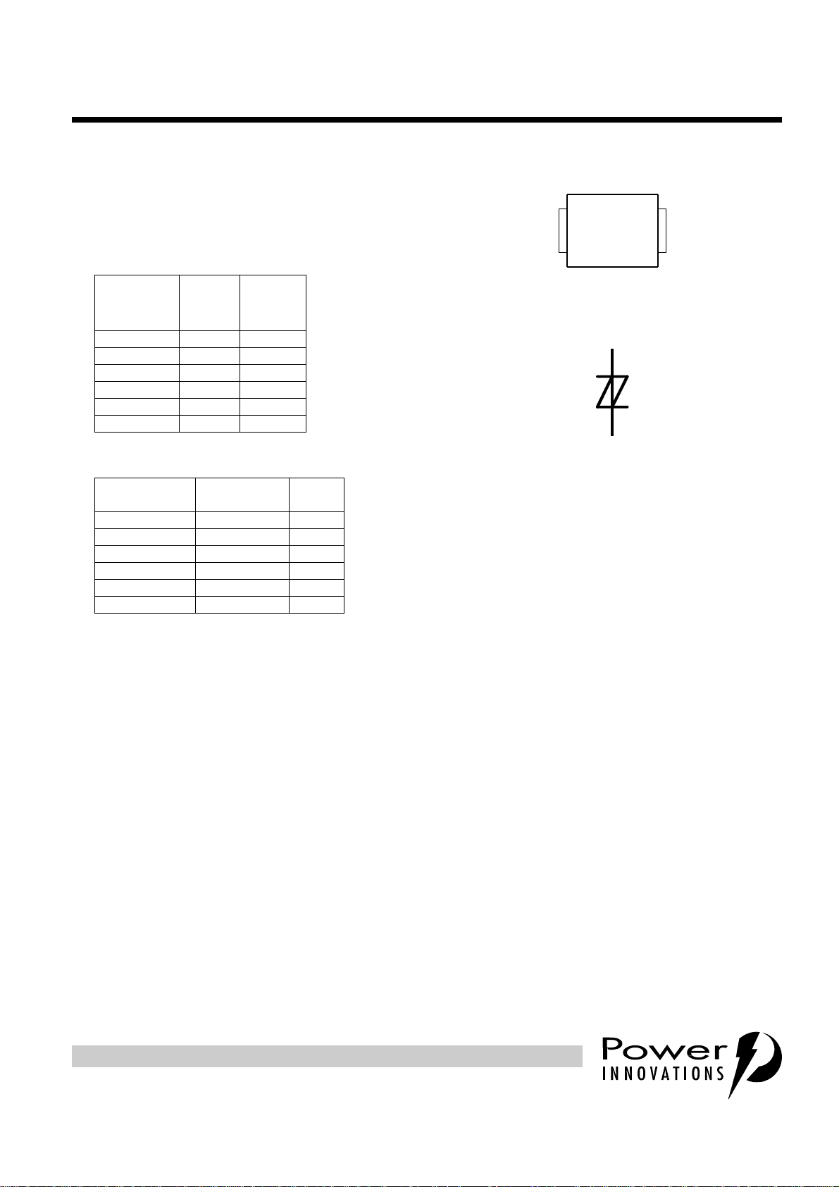
device symbol
BIDIRECTIONAL THYRISTOR OVERVOLTAGE PROTECTORS
HIGH HOLDING CURRENT 100 A 10/1000 OVERVOLTAGE PROTECTORS
●
8 kV 10/700, 200 A 5/310 ITU-T K20/21 rating
●
High Holding Current . . . . . . . . . 225 mA min.
●
Ion-Implanted Breakdown Region
Precise and Stable Voltage
Low Voltage Overshoot under Surge
V
DRM
DEVICE
‘4165 135 165
‘4180 145 180
‘4200 155 200
‘4265 200 265
‘4300 230 300
‘4360 270 360
●
Rated for International Surge Wave Shapes
WAV E SHAP E STANDARD
2/10 µs GR-1089-CORE 500
8/20 µs IEC 61000-4-5 300
10/160 µs FCC Part 68 250
10/700 µs ITU-T K20/21 200
10/560 µs FCC Part 68 160
10/1000 µs GR-1089-CORE 100
MINIMUM
V
V
(BO)
MAXIMUM
V
I
TSP
A
NOVEMBER 1997 - REVISED MARCH 1999Copyright © 1999, Power Innovations Limited, UK
SMBJ PACKAGE
(TOP VIEW)
12
T
R
Terminals T and R correspond to the
alternative line designators of A and B
T(A)R(B)
MDXXBG
SD4XAA
●
description
Low Differential Capacitance . . . 39 pF max.
These devices are designed to limit overvoltages on the telephone line. Overvoltages are normally caused by
a.c. power system or lightning flash disturbances whic h ar e ind uc ed or co ndu cte d on to the telephone li ne. A
single device provides 2-point protection and is typically u sed for the protec tion of 2 -wire tel ecommunicatio n
equipment (e.g. between the Ri ng and Tip wires for telephones a nd modems ). Combinati ons of devices ca n
be used for multi-point protection (e.g. 3-point protection between Ring, Tip and Ground).
The protector consists of a symmetrical voltage-triggered bidirectional thyristor. Overvoltages are initially
clipped by breakdown clamping until the voltage rises to the breakover level, which causes the device to
crowbar into a low-voltage on state. This low-voltage on state causes the current resulting from the
overvoltage to be safely diverted through the device. The high crowbar holding cu rrent prevents d.c. latchup
as the diverted current subsides.
This TISP4xxxH4BJ range consists of six voltage variants to meet various maxi mum system voltage levels
(135 V to 270 V). They are guaranteed to voltage li mit and withs tand the li sted inter nat ional li ghtning sur ges
in both polar ities. These high (H) current p rotection d evices are in a plastic package SMBJ (JEDEC DO214AA with J-bend l eads) and supplied i n embossed carrier reel pack. For alternative voltage and holdin g
current values, consult the factory. For lower rated impulse curren ts in the SMB package, the 50 A 10/1000
TISP4xxxM3BJ series is available.
PRODUCT INFORMATION
Information is current as of publication date. Produc ts conform to specifications in accordance
with the terms of Power Innovations standard warranty. Production processing does not
necessarily include testing of all parameters.
1
Page 2

TISP4165H4BJ THRU TISP4200H4BJ, TISP4265H4BJ THRU TISP4360H4BJ
BIDIRECTIONAL THYRISTOR OVERVOLTAGE PROTECTORS
NOVEMBER 1997 - REVISED MARCH 1999
T
absolute maximum ratings,
Repetitive peak off-state voltage, (see Note 1)
Non-repetitive peak on-state pulse current (see Notes 2, 3 and 4)
2/10 µs (GR-1089-CORE, 2/10 µs voltage wave shape) 500
8/20 µs (IEC 61000-4-5, 1.2/50 µs voltage, 8/20 current combination wave generator) 300
10/160 µs (FCC Part 68, 10/160 µs voltage wave shape) 250
5/200 µs (VDE 0433, 10/700 µs voltage wave shape) 220
0.2/310 µs (I3124, 0.5/700 µs voltage wave shape) 200
5/310 µs (ITU-T K20/21, 10/700 µs voltage wave shape) 200
5/310 µs (FTZ R12, 10/700 µs voltage wave shape) 200
10/560 µs (FCC Part 68, 10/560 µs voltage wave shape) 160
10/1000 µs (GR-1089-CORE, 10/1000 µs voltage wave shape) 100
Non-repetitive peak on-state current (see Notes 2, 3 and 5)
20 ms (50 Hz) full sine wave
16.7 ms (60 Hz) full sine wave
1000 s 50 Hz/60 Hz a.c.
Initial rate of rise of on-state current, Exponential current ramp, Maximum ramp value < 200 A di
Junction temperature T
Storage temperature range T
= 25°C (unless otherwise noted)
A
RATING SYMBOL VALUE UNIT
‘4165
‘4180
‘4200
‘4265
‘4300
‘4360
V
DRM
I
TSP
I
TSM
/dt 400 A/µs
T
J
stg
±135
±145
±155
±200
±230
±270
55
60
2.1
-40 to +150 °C
-65 to +150 °C
V
A
A
NOTES: 1. See Applications Information and Figure 10 for voltage values at lower temperatures.
2. Initially the TISP4xxxH4BJ must be in thermal equilibrium with T
3. The surge may be repeated after the TISP4xxxH4BJ returns to its initial conditions.
4. See Applications Information and Figure 11 for current ratings at other temperatures.
5. EIA/JESD51-2 environment and EIA/JESD51-3 PCB with standard footprint dimensions connected with 5 A rated printed wiring
track widths. See Figure 8 for the current ratings at other durations. Derate current v alues at -0.61%/°C for ambient temperatures
above 25 °C
=25°C.
J
PRODUCT INFORMATION
2
Page 3

TISP4165H4BJ THRU TISP4200H4BJ, TISP4265H4BJ THRU TISP4360H4BJ
BIDIRECTIONAL THYRISTOR OVERVOLTAGE PROTECTORS
NOVEMBER 1997 - REVISED MARCH 1999
electrical characterist ics for the T and R terminals, TA = 25°C (unless otherwise noted)
PARAMETER TEST CONDITIONS MIN TYP MAX UNIT
I
DRM
V
(BO)
V
(BO)
I
(BO)
V
T
I
H
dv/dt
I
D
C
off
Repetitive peak offstate current
Breakover voltage dv/dt = ±750 V/ms, R
V
= ±V
D
DRM
SOURCE
= 300
Ω
dv/dt≤±1000 V/µs, Linear voltage ramp,
Impulse breakover
voltage
Maximum ramp value = ±500 V
di/dt = ±20 A/µs, Linear current ramp,
Maximum ramp value = ±10 A
Breakover current dv/dt = ±750 V/ms, R
SOURCE
= 300
Ω
On-state voltage IT=±5A, tW= 100 µs ±3 V
Holding current IT= ±5 A, di/dt = +/-30 mA/ms ±0.225 ±0.8 A
Critical rate of rise of
off-state voltage
Linear voltage ramp, Maximum ramp value < 0.85V
DRM
Off-state current VD=±50V TA = 85°C ±10 µA
Off-state capacitance
f = 100 kHz, V
f = 100 kHz, V
f = 100 kHz, V
f = 100 kHz, V
f = 100 kHz, V
=1V rms, VD=0,
d
=1V rms, VD=-1V
d
=1V rms, VD=-2V
d
=1V rms, VD=-50V
d
=1V rms, VD= -100 V
d
TA = 25°C
= 85°C
T
A
‘4165
‘4180
‘4200
‘4265
‘4300
‘4360
‘4165
‘4180
‘4200
‘4265
‘4300
‘4360
‘4165 thru ‘4200
‘4265 thru ‘4360
‘4165 thru ‘4200
‘4265 thru ‘4360
‘4165 thru ‘4200
‘4265 thru ‘4360
‘4165 thru ‘4200
‘4265 thru ‘4360
‘4165 thru ‘4200
‘4265 thru ‘4360
±0.15 ±0.8 A
±5 kV/µs
80
70
71
60
65
55
30
24
28
22
±5
±10
±165
±180
±200
±265
±300
±360
±174
±189
±210
±276
±311
±373
90
84
79
67
74
62
35
28
33
26
µA
V
V
pF
thermal characteristics
PARAMETER
EIA/JESD51-3 PCB, I
= 25 °C, (see Note 6)
T
R
Junction to free air thermal resistance
θ
JA
A
265 mm x 210 mm populated line card,
4-layer PCB, I
TEST CONDITIONS
= I
T
TSM(1000)
= I
T
TSM(1000)
, TA = 25 °C
,
NOTE 6: EIA/JESD51-2 environment and PCB has standard footprint dimensions connected with 5 A rated printed wiring track widths.
MIN TYP MAX UNIT
113
°C/W
50
PRODUCT INFORMATION
3
Page 4
TISP4165H4BJ THRU TISP4200H4BJ, TISP4265H4BJ THRU TISP4360H4BJ
BIDIRECTIONAL THYRISTOR OVERVOLTAGE PROTECTORS
NOVEMBER 1997 - REVISED MARCH 1999
PARAMETER MEASUREMENT INFORMATION
-v
I
DRM
I
(BO)
V
Quadrant III
Switching
Characteristic
(BO)
+i
I
TSP
Characteristic
I
TSM
I
T
V
T
I
H
V
DRM
V
D
I
D
I
D
I
H
V
T
I
T
I
TSM
I
TSP
V
D
-i
Quadrant I
Switching
V
DRM
V
(BO)
I
DRM
PMXXAAB
I
(BO)
+v
Figure 1. VOLTAGE-CURRENT CHARACTERISTIC FOR T AND R TERMINALS
ALL MEASUREMENTS ARE REFERENCED TO THE R TERMINAL
PRODUCT INFORMATION
4
Page 5
100
NORMALISED BREAKOVER VOLTAGE
vs
JUNCTION TEMPERATURE
TJ - Junction Temperature - °C
-25 0 25 50 75 100 125 150
Normalised Breakover Voltage
0.95
1.00
1.05
1.10
TC4HAF
NORMALISED HOLDING CURRENT
vs
JUNCTION TEMPERATURE
TJ - Junction Temperature - °C
-25 0 25 50 75 100 125 150
Normalised Holdi ng Current
0.4
0.5
0.6
0.7
0.8
0.9
1.5
2.0
1.0
TC4HAK
10
0·1
| - Off-State Current - µA
D
|I
0·01
VD = ±50 V
1
TISP4165H4BJ THRU TISP4200H4BJ, TISP4265H4BJ THRU TISP4360H4BJ
BIDIRECTIONAL THYRISTOR OVERVOLTAGE PROTECTORS
TYPICAL CHARACTERISTICS
OFF-STATE CURRENT
vs
JUNCTION TEMPERATURE
NOVEMBER 1997 - REVISED MARCH 1999
TCHAG
0·001
-25 0 25 50 75 100 125 150
TJ - Junction Temperature - °C
Figure 2. Figure 3.
ON-STATE CURRENT
ON-STATE VOLTAGE
200
150
TA = 25 °C
t
100
- On-State Current - A
T
I
= 100 µs
W
70
50
40
30
20
15
10
7
5
4
3
2
1.5
1
0.7 1.5 2 3 4 5 7110
'4265
THRU
'4360
VT - On-State Voltage - V
Figure 4. Figure 5.
vs
'4165
THRU
'4200
TC4HAH
PRODUCT INFORMATION
5
Page 6

TISP4165H4BJ THRU TISP4200H4BJ, TISP4265H4BJ THRU TISP4360H4BJ
BIDIRECTIONAL THYRISTOR OVERVOLTAGE PROTECTORS
NOVEMBER 1997 - REVISED MARCH 1999
TYPICAL CHARACTERISTICS
NORMALISED CAPACITANCE
vs
OFF-STATE VOLTAGE
1
0.9
0.8
= 0
0.7
D
0.6
0.5
'4265 THRU '4360
0.4
0.3
Capacitance Normalised to V
0.2
0.5 1 2 3 5 10 20 30 50 100150
VD - Off-state Voltage - V
TJ = 25°C
V
= 1 Vrms
d
'4165 THRU '4200
Figure 6. Figure 7.
TC4HAI
DIFFERENTIAL OFF-STATE CAPACITANCE
vs
RATED REPETITIVE PEAK OFF-STATE VOLTAGE
36
35
'4165
'4180
'4200
34
33
∆∆∆∆C = C
32
31
C - Differential Off-State Capacitan ce - pF
∆
∆∆
∆
30
130 150 170 200 230 270 300
V
- Repetitive P eak Off-State Voltage - V
DRM
off(-2 V)
'4265
- C
'4300
off(-50 V)
TCHAJ
'4360
PRODUCT INFORMATION
6
Page 7

TISP4165H4BJ THRU TISP4200H4BJ, TISP4265H4BJ THRU TISP4360H4BJ
THERMAL IMPEDANCE
vs
POWER DURATION
t - Power Duration - s
0·1 1 10 100 1000
Z
θ
θθ
θ
JA(t)
- Transient Thermal Impedance - °C/W
1.5
2
3
4
5
7
15
20
30
40
50
70
150
1
10
100
TI4HAE
I
TSM(t)
APPLIED FOR TIME t
EIA/JESD51-2 ENVIRONMENT
EIA/JESD51-3 PCB
T
A
= 25 °C
IMPULSE RATING
vs
AMBIENT TEMPERATURE
TA - Ambient Temperature - °C
-40-30-20-100 1020304050607080
Impulse Current - A
90
100
120
150
200
250
300
400
500
600
700
IEC 1.2/50, 8/20
ITU-T 10/700
FCC 10/560
BELLCORE 2/10
BELLCORE 10/1000
FCC 10/160
TC4HAA
BIDIRECTIONAL THYRISTOR OVERVOLTAGE PROTECTORS
RATING AND THERMAL INFORMATION
NON-REPETITIVE PEAK ON-STATE CURRENT
vs
30
20
15
10
CURRENT DURATION
V
= 600 Vrms, 50/60 Hz
GEN
= 1.4*V
R
GEN
EIA/JESD51-2 ENVIRONMENT
EIA/JESD51-3 PCB
T
= 25 °C
A
9
8
7
6
5
4
3
GEN
/I
TSM(t)
TI4HAC
NOVEMBER 1997 - REVISED MARCH 1999
- Non-Repetitive P eak On-State Current - A
2
TSM(t)
I
1.5
0·1 1 10 100 1000
t - Current Duration - s
Figure 8. Figure 9.
V
DERATING FACTOR
DRM
vs
MINIMUM AMBIENT TEMPERATURE
1.00
0.99
0.98
0.97
'4165 THRU '4200
0.96
Derating Factor
0.95
0.94
0.93
PRODUCT INFORMATION
'4265 THRU '4360
-35 -25 -15 -5 5 15 25-40 -30 -20 -10 0 10 20
T
- Minimum Ambient Temperature - °C
AMIN
Figure 10. Figure 11.
TI4HAF
7
Page 8

TISP4165H4BJ THRU TISP4200H4BJ, TISP4265H4BJ THRU TISP4360H4BJ
Th3
Th2
Th1
BIDIRECTIONAL THYRISTOR OVERVOLTAGE PROTECTORS
NOVEMBER 1997 - REVISED MARCH 1999
APPLICATIONS INFORMATION
deployment
These devices are two terminal overvoltage prote ctors. They may be used either singly to limit the voltage
between two conductors (Figure 12) or in multiples to limit the voltage at several points in a circuit (Figure 13).
Th1
Figure 12. TWO POINT PROTECTION Figure 13. MULTI-POINT PROTECTION
In Figure 12, protector Th1 limits the maximum voltage between the two conductors to ±V
configuration is nor mall y used to protect ci rcuits withou t a ground reference, such as modems. In Figure 1 3,
protectors Th2 and Th3 lim it the maximum voltage be tween each cond uctor and ground to the ±V
individual protector. Protector Th1 limits the maximum voltage between the two conductors to its ±V
value. If the equipment being protected has all its vulnerable components connected between the conductors
and ground, then protector Th1 is not required.
impulse testing
To verify the wit hstand capabil ity and safety of the equipment , standards require that the equipm ent is test ed
with various impulse wave forms. The table below shows some common values.
PEAK VOLTAGE
STANDARD
GR-1089-CORE
FCC Part 68
(March 1998)
I3124 1500 0.5/700 37.5 0.2/310 200 0
ITU-T K20/K21
† FCC Part 68 terminology for the waveforms produced by the ITU-T recommendation K21 10/700 impulse generator
SETTING
V
2500 2/10 500 2/10 500
1000 10/1000 100 10/1000 100
1500 10/160 200 10/160 250 0
800 10/560 100 10/560 160 0
1500 9/720 † 37.5 5/320 † 200 0
1000 9/720 † 25 5/320 † 200 0
1500
4000
VOLTAGE
WAVE FORM
µs
10/700
PEAK CURRENT
VALUE
A
37.5
100
CURRENT
WAVE FORM
µs
5/310 200 0
TISP4xxxH4
25 °C RATING
A
SERIES
RESISTANCE
Ω
0
(BO)
(BO)
. This
of the
(BO)
If the impulse generator current exceeds the protectors current rating then a series resistance can be used to
reduce the curren t to the prot ectors rat ed value and so prevent possible failure. The required value of se rie s
resistance for a given waveform is given by the following calculations. First, the minimum total circuit
impedance is found by dividing the impulse generators peak voltage by the protectors rated current. The
impulse generators fictive impedance (generators pea k voltage divided by peak shor t circuit current) is then
subtracted from the m inimum total circ uit impe dance to give the requi red value of s eri es res istance. In so me
cases the equipme nt will require verifi cation over a temperature range. By usin g the rated waveform values
from Figure 11, the appropriate series resistor value can be calculated for ambient temperatures in the range
of -40 °C to 85 °C.
PRODUCT INFORMATION
8
Page 9

TISP4165H4BJ THRU TISP4200H4BJ, TISP4265H4BJ THRU TISP4360H4BJ
BIDIRECTIONAL THYRISTOR OVERVOLTAGE PROTECTORS
NOVEMBER 1997 - REVISED MARCH 1999
a.c. power testing
The protector can withstan d currents applied for times not exceeding thos e shown in Figure 8 . Currents tha t
exceed these times must be terminated or reduced to avoid protector failure. Fuses, PTC (Positive
Temperature Coefficient) resistors and fusible resistors are overcurrent protection devices which can be used
to reduce the current fl ow. Protective fuses may range from a few hundred milliamperes to o ne ampere. In
some cases it may be necessa ry to add some extra seri es resistance to prevent the fuse opening dur ing
impulse testing. The current versus time cha racteristic of the overcurrent protector must be below the line
shown in Figure 8. In some ca ses there may be a further time limit imposed by the test standard ( e.g. UL
1459 wiring simulator failure).
capacitance
The protector characteristic off-state capacitance values are given for d.c. bias voltage, VD, values of 0, -1 V,
-2 V and - 50 V. Where possible values are also given for -100 V. Values for other voltages may be calculate d
by multiplying the V
essentially independent of frequency. Above 10 MHz the effective capacitance is strongly dependent on
connection inducta nce. In many applications, such as Figur e 15 and Figure 17, the typic al conductor bias
voltages will be about -2 V a nd -5 0 V. Figure 7 shows the di fferential (lin e u nbalance) capacitanc e c aus ed by
biasing one protector at -2 V and the other at -50 V.
= 0 ca pacit ance value by the factor given in Figure 6. Up to 10 MHz the capac itance is
D
normal system voltage levels
The protector should not clip or limit the voltages that occur in normal system operation. For unusual
conditions, such as r inging without the line connected , some degree of clipping is per missible. Under this
condition about 10 V of clipping is normally possible without activating the ring trip circuit.
Figure 10 allows the calculation of the protector V
value should not be less than the maximum nor mal system voltages. The TISP4265H4BJ, with a V
200 V, can be used for the protection of ring generators producing 100 V rms of ring on a battery voltage of
-58 V (Th2 and Th3 in Figure 17). The peak ring voltage will be 58 + 1.414*100 = 199.4 V. Howe v er, this is the
open circuit voltage and the connec tion of the line and its equipment will reduce the pe ak voltage. In the
extreme case of an unconnected line, clipping the peak voltage to 190 V should not activate the ring trip. This
level of clipping would occur at the temperature when the V
value. Figure 10 shows that this condition will occur at an ambient temperature of -22 °C. In this example, the
TISP4265H4BJ will allow normal equipment operation provided that the minimum expected ambient
temperature does not fall below -22 °C.
value at temperatures below 25 °C. The calculated
DRM
has reduced to 190/2 00 = 0.95 of its 25 °C
DRM
JESD51 thermal measurement method
To standardise thermal measurements, the EIA (Electronic Industries Alliance) has created the JESD51
standard. Part 2 of the standard (JESD51-2, 1995) describes the test environment. This is a 0.0283 m
cube which contains the test PCB (Printed Ci rcuit Board) horizontally mou nted at the centre. Part 3 of the
standard (JESD51-3, 199 6) defines two test PCB s for surface mount components; one for packages smaller
than 27 mm on a side and the o ther for packages up to 48 mm. The SMBJ me asureme nts used th e small er
76.2 mm x 114.3 mm (3.0 “ x 4.5 “) PCB. The JESD51-3 PCBs are d esigned to have low effective thermal
conductivity (high th er mal resi stance) and represen t a worse case con dition . The PCBs us ed in the ma jority
of applications will a chieve lower values of thermal resis tance and s o can dis sipate higher power levels than
indicated by the JESD51 values.
DRM
3
(1 ft3)
of
PRODUCT INFORMATION
9
Page 10

TISP4165H4BJ THRU TISP4200H4BJ, TISP4265H4BJ THRU TISP4360H4BJ
BIDIRECTIONAL THYRISTOR OVERVOLTAGE PROTECTORS
NOVEMBER 1997 - REVISED MARCH 1999
typical circuits
RING
TIP
FUSE
TISP4360H4
MODEM
RING DETECTOR
HOOK SWITCH
D.C. SINK
SIGNAL
AI6XBP
TIP
WIRE
RING
WIRE
R1a
Th1
R1b
Th3
Th2
PROTECTED
EQUIPMENT
E.G. LINE CARD
Figure 14. MODEM INTER-WIRE PROTECTION Figure 15. PROTECTION MODULE
R1a
Th3
Th1
Th2
R1b
D.C.
SIGNAL
AI6XBL
Figure 16. ISDN PROTECTION
AI6XBK
TIP
WIRE
RING
WIRE
OVER-
CURRENT
PROTECTION
R1a
R1b
RING/TEST
PROTECTION
Th3
Th1
Th2
TEST
RELAY
S1a
S1b
TEST
EQUIP-
MENT
RING
RELAY
S2a
S2b
RING
GENERATOR
Figure 17. LINE CARD RING/TEST PROTECTION
SLIC
RELAY
S3a
S3b
SLIC
PROTECTION
Th4
Th5
TISP6xxxx,
TISPPBLx,
½TISP6NTP2
C1
220 nF
SLIC
V
BAT
AI6XBJ
PRODUCT INFORMATION
10
Page 11

TISP4165H4BJ THRU TISP4200H4BJ, TISP4265H4BJ THRU TISP4360H4BJ
BIDIRECTIONAL THYRISTOR OVERVOLTAGE PROTECTORS
NOVEMBER 1997 - REVISED MARCH 1999
MECHANICAL DATA
SMBJ (DO-214AA)
plastic surface mount diode package
This surface mount package consist s of a circ uit moun ted on a lea d frame and en caps ulated within a pl astic
compound. The compound will withstand soldering temperature with no deformation, and circuit performance
characteristics will remain stable when operated in high humidity conditions. Leads require no additional
cleaning or processing when used in soldered assembly.
SMB
4,57
4,06
3,94
3,30
2,40
2,00
1,52
0,76
Index
Mark
(if needed)
2,10
1,90
5,59
5,21
2
0,20
0,10
2,32
1,96
ALL LINEAR DIMENSIONS IN MILLIMETERS
PRODUCT INFORMATION
MDXXBHA
11
Page 12

TISP4165H4BJ THRU TISP4200H4BJ, TISP4265H4BJ THRU TISP4360H4BJ
BIDIRECTIONAL THYRISTOR OVERVOLTAGE PROTECTORS
NOVEMBER 1997 - REVISED MARCH 1999
MECHANICAL DATA
recommended printed wiring footprint.
SMB Pad Size
2.54
2.40
2.16
ALL LINEAR DIMENSIONS IN MILLIMETERS
MDXXBI
device symbolization code
Devices will be coded as below. As the device parameters are symmetrical, terminal 1 is not identified.
DEVICE
TISP4165H4BJ 4165H4
TISP4180H4BJ 4180H4
TISP4200H4BJ 4200H4
TISP4265H4BJ 4265H4
TISP4300H4BJ 4300H4
TISP4360H4BJ 4360H4
SYMOBLIZATION
CODE
carrier info r m a tion
Devices are shipped in on e of the carriers be low. Unless a specific method of shipment is s pecified by the
customer, devices will be shipped in the most practical carrier. For production quantities the carr ier will be
embossed tape reel pack. Evaluation quantities may be shipped in bulk pack or embossed tape.
CARRIER ORDER #
Embossed Tape Reel Pack TISP 4xx xH4BJ R
Bulk Pack TISP4xxxH4BJ
PRODUCT INFORMATION
12
Page 13

TISP4165H4BJ THRU TISP4200H4BJ, TISP4265H4BJ THRU TISP4360H4BJ
tape dimensions
SMB Package Single-Sprocket Tape
BIDIRECTIONAL THYRISTOR OVERVOLTAGE PROTECTORS
NOVEMBER 1997 - REVISED MARCH 1999
MECHANICAL DATA
8,10
7,90
Direction of Feed
4,10
3,90
2,05
1,95
ø 1,5 MIN.
Carrier Tape
Embossment
Index
Mark
(if needed)
1,65
1,55
20°
1,85
1,65
5,55
5,45
0 MIN.
Maximium com ponent
rotation
Typical compon ent
cavity centre line
Typical compon ent
centre line
0,40 MAX.
12,30
11,70
Cover
Tape
8,20
MAX.
4,5 MAX.
ALL LINEAR DIMENSIONS IN MILLIMETERS
NOTES: A. The clearance between the component and the cavity must be within 0,05 mm MIN. to 0,65 mm MAX. so that the
component cannot rotate more than 20° within the determined cavity.
B. Taped devices are supplied on a reel of the following dimensions:-
R e el di am et e r: 330 ±3,0 mm
Reel hub diameter 75 mm MIN.
Reel axial hole: 13,0 ±0,5 mm
C.
3000 devices are on a reel.
PRODUCT INFORMATION
MDXXBJ
13
Page 14

TISP4165H4BJ THRU TISP4200H4BJ, TISP4265H4BJ THRU TISP4360H4BJ
BIDIRECTIONAL THYRISTOR OVERVOLTAGE PROTECTORS
NOVEMBER 1997 - REVISED MARCH 1999
IMPORTANT NOTICE
Power Innovations Limited (PI) re se rves the r ig ht t o make chan g es t o it s pr od uc ts o r t o di sc ont inu e any s em ic o nduc t or p r o duct
or service without notice, and advises its customers to verify, before placing orders, that the information being relied on is
current.
PI warrants performance of its semiconductor products to the specifications applicable at the time of sale in accordance with
PI's standard w arr anty. Testing and other quality cont rol tec hn iqu es are uti li z ed to the exten t PI deems necessary to support this
warranty. Specific testing of all parameters of each device is not necessarily performed, except those mandated by government
requirements.
PI assumes no liability for applications assistance, customer product design, software performance, or infringement of patents
or services described herein. Nor is any license, either express or implied, granted under any patent right, copyright, design
right, or other intellectual property right of PI covering or relating to any combination, machine, or process in which such
semiconductor products or services might be or are used.
PI SEMICONDUCTOR PRODUCTS ARE NOT DESIGNED, INTENDED, AUTHORISED, OR WARRANTED TO BE SUITABLE
FOR USE IN LIFE-SUPPORT APPLICATIONS, DEVICES OR SYSTEMS.
Copyright © 1999, Power Innovations Limited
PRODUCT INFORMATION
14
 Loading...