

Datasheet TISP4260F3LM, TISP4380F3LM, TISP4290F3LM, TISP4320F3LM, TISP4082F3LM Datasheet (Power Innovations)
...Page 1
TISP4072F3LM, TISP4082F3LM, TISP4125F3LM, TISP4150F3LM, TISP4180F3LM
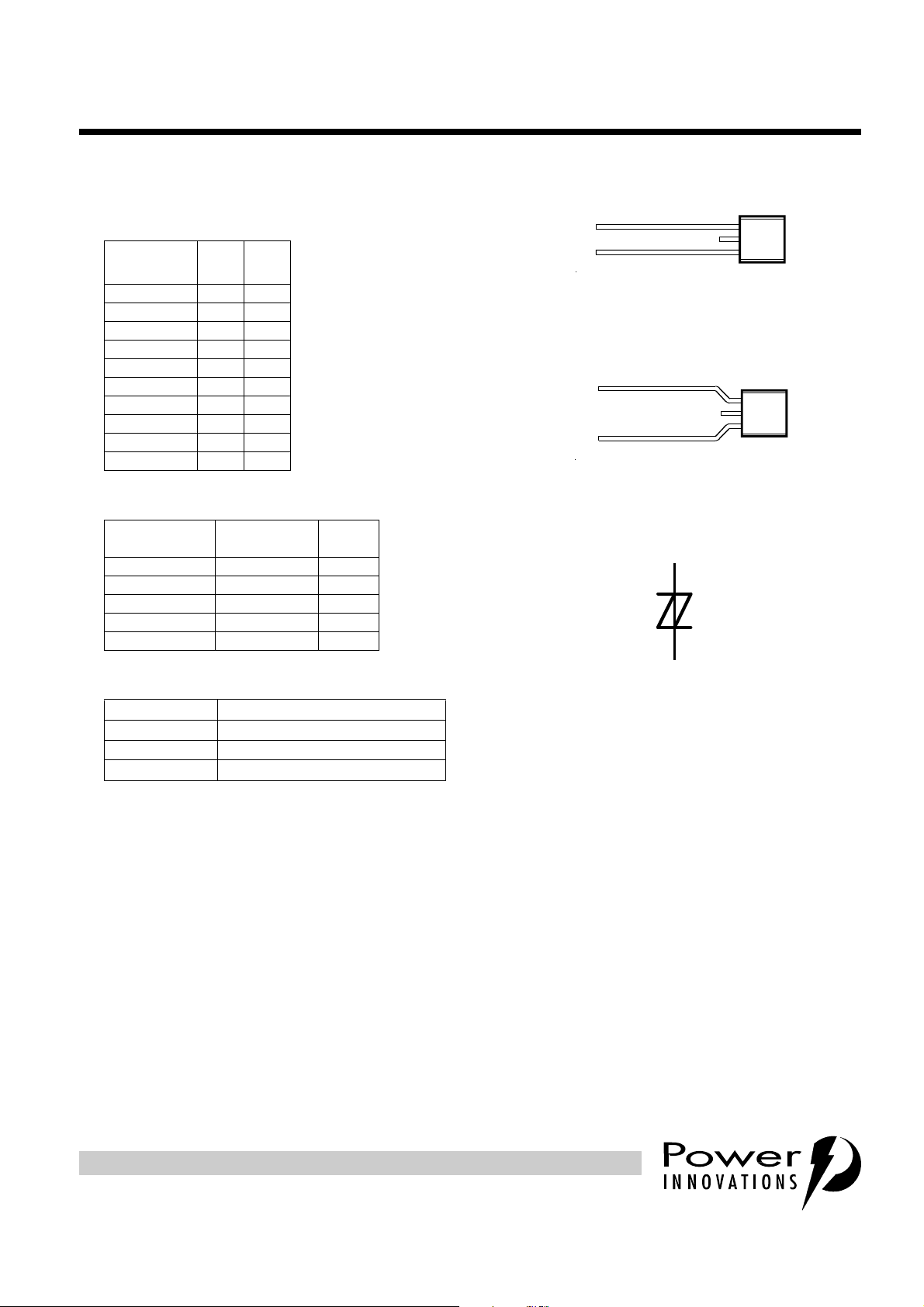
device symbol
LMF PACKAGE
(LM PACKAGE WITH FORMED LEADS)
(TOP VIEW)
NC - No internal connection on pin 2
NC
T(A)
R(B)
MD4XAKB
1
2
3
LM PACKAGE
(TOP VIEW)
NC - No internal connection on pin 2
NC
T(A)
R(B)
MD4XAT
1
2
3
TISP4240F3LM, TISP4260F3LM, TISP4290F3LM, TISP4320F3LM, TISP4380F3LM
TELECOMMUNICATION SYSTEM SECONDARY PROTECTION
●
Ion-Implanted Breakdown Region
Precise and Stable Voltage
Low Voltage Overshoot under Surge
BIDIRECTIONAL THYRISTOR OVERVOLTAGE PROTECTORS
DECEMBER 1998 - REVISED APRIL 1999Copyright © 1999, Power Innovations Limited, UK
DRM
V
V
(BO)
V
I
TSP
A
DEVICE
‘4072 58 72
‘4082 66 82
‘4125 100 125
‘4150 120 150
‘4180 145 180
‘4240 180 240
‘4260 200 260
‘4290 220 290
‘4320 240 320
‘4380 270 380
●
Rated for International Surge Wave Shapes
WAV E SHAP E STANDARD
10/160 µs FCC Part 68 60
0.5/700 µs I3124 38
10/700 µs ITU-T K20/21 50
10/560 µs FCC Part 68 45
10/1000 µs REA PE-60 35
●
Ordering Information
DEVICE TYPE PACKAGE TYPE
TISP4xxxF3LM Straight Lead DO-92 Bulk Pack
TISP4xxxF3LMR Straight Lead DO-92 Tape and Reeled
TISP4xxxF3LMFR Formed Lead DO-92 Tape and Reeled
V
T
R
Terminals T and R correspond to the
alternative line designators of A and B
SD4XAA
description
PRODUCT INFORMATION
Information is current as of publication date. Produc ts conform to specifications in accordance
with the terms of Power Innovations standard warranty. Production processing does not
necessarily include testing of all parameters.
These devices are designed to limit overvoltages on the telephone line. Overvoltages are normally caused by
a.c. power system or lightning flash disturbances whic h ar e ind uc ed or co ndu cte d on to the telephone li ne. A
single device provides 2-point protection and is typically u sed for the protec tion of 2 -wire tel ecommunicatio n
equipment (e.g. between the Ring to Tip wires for telephones and modems). Combinations of devices can be
used for multi-point protection (e.g. 3-point protection between Ring, Tip and Ground).
The protector consists of a symmetrical voltage-triggered bidirectional thyristor. Overvoltages are initially
clipped by breakdown clamping until the voltage rises to the breakover level, which causes the device to
crowbar into a low-voltage on state. This low-voltage on state causes the current resulting from the
overvoltage to be safely diverted through the device. The high crowbar holding cu rrent prevents d.c. latchup
as the diverted current subsides.
This TISP4xxxF3LM range consists of te n voltage variants to meet various maximum s ystem voltage levels
(58 V to 270 V). They are guaranteed to voltage limit and withstand the listed international lightning surges in
both polarities. These protection devices are supplied in a DO-92 (LM) cylindrical plastic package. The
1
Page 2

TISP4072F3LM, TISP4082F3LM, TISP4125F3LM, TISP4150F3LM, TISP4180F3LM
)
TISP4240F3LM, TISP4260F3LM, TISP4290F3LM, TISP4320F3LM, TISP4380F3LM
BIDIRECTIONAL THYRISTOR OVERVOLTAGE PROTECTORS
DECEMBER 1998 - REVISED APRIL 1999
description (continued
TISP4xxxF3LM is a straigh t lead DO- 92 sup plied in bulk pack and on ta pe and r eeled . The TISP4xx xF3LMF
is a formed lead DO-92 supplied only on tape and reeled.
absolute maximum ratings
RATING SYMBOL VALUE UNIT
‘4072
‘4082
‘4125
‘4150
Repetitive peak off-state voltage (0 °C < T
Non-repetitive peak on-state pulse current (see Notes 1, 2 and 3)
2/10 µs (FCC Part 68, 2/10 µs voltage wave shape) excluding ‘4072 - ‘4082 175
8/20 µs (ANSI C62.41, 1.2/50 µs voltage wave shape) excluding ‘4072 - ‘4082 120
10/160 µs (FCC Part 68, 10/160 µs voltage wave shape) 60
5/200 µs (VDE 0433, 2 kV, 10/700 µs voltage wave shape) 50
0.2/310 µs (I3124, 1.5 kV, 0.5/700 µs voltage wave shape) 38
5/310 µs (ITU-T K20/21, 1.5 kV, 10/700 µs voltage wave shape) 38
5/310 µs (FTZ R12, 2 kV, 10/700 µs voltage wave shape) 50
10/560 µs (FCC Part 68, 10/560 µs voltage wave shape) 45
10/1000 µs (REA PE-60, 10/1000 µs voltage wave shape) 35
2/10 µs (FCC Part 68, 2/10 µs voltage wave shape) ‘4072 - ‘4082 only 80
8/20 µs (ANSI C62.41, 1.2/50 µs voltage wave shape) ‘4072 - ‘4082 only 70
Non-repetitive peak on-state current (see Notes 2 and 3)
50/60 Hz, 1 s
Initial rate of rise of on-state current, Linear current ramp, Maximum ramp value < 38 A di
Junction temperature T
Storage temperature range T
< 70 °C)
J
‘4180
‘4240
‘4260
‘4290
‘4320
‘4380
V
DRM
I
TSP
I
TSM
/dt 250 A/µs
T
J
stg
± 58
± 66
± 100
± 120
± 145
± 180
± 200
± 220
± 240
± 270
4A
-40 to +150 °C
-55 to +150 °C
V
A
NOTES: 1. Initially the TISP must be in thermal equilibrium with 0 °C < TJ<70°C.
2. The surge may be repeated after the TISP returns to its initial conditions.
3. Above 70 °C, derate linearly to zero at 150 °C lead temperature.
PRODUCT INFORMATION
2
Page 3

TISP4072F3LM, TISP4082F3LM, TISP4125F3LM, TISP4150F3LM, TISP4180F3LM
TISP4240F3LM, TISP4260F3LM, TISP4290F3LM, TISP4320F3LM, TISP4380F3LM
BIDIRECTIONAL THYRISTOR OVERVOLTAGE PROTECTORS
DECEMBER 1998 - REVISED APRIL 1999
electrical characterist ics for the T and R terminals, TJ = 25 °C (unless otherwise noted)
PARAMETER TEST CONDITIONS MIN TYP MAX UNIT
I
V
V
I
V
I
dv/dt
I
C
Repetitive peak off-
DRM
state current
Breakover voltage dv/dt = ±250 V/ms, R
(BO)
Impulse breakover
(BO)
voltage
Breakover current dv/dt = ±250 V/ms, R
(BO)
On-state voltage IT=±5A, tW= 100 µs ±3 V
T
Holding current IT= ±5 A, di/dt = +/-30 mA/ms ±0.15 A
H
Critical rate of rise of
off-state voltage
Off-state current VD=±50V ±10 µA
D
Off-state capacitance
off
= ±V
V
D
dv/dt = ±1000 V/µs, R
di/dt < 20 A/µs
Linear voltage ramp, Maximum ramp value < 0.85V
f = 100 kHz, V
f = 100 kHz, V
, 0 °C < TJ < 70 °C ±10 µA
DRM
Ω
= 300
SOURCE
Ω,
=50
SOURCE
Ω
= 300
SOURCE
= 1 Vrms, VD=0,
d
= 1 Vrms, VD=-50V
d
DRM
‘4072
‘4082
‘4125
‘4150
‘4180
‘4240
‘4260
‘4290
‘4320
‘4380
‘4072
‘4082
‘4125
‘4150
‘4180
‘4240
‘4260
‘4290
‘4320
‘4380
‘4072 - ‘4082
‘4125 - ‘4180
‘4240 - ‘4380
‘4072 - ‘4082
‘4125 - ‘4180
‘4240 - ‘4380
±0.15 ±0.6 A
±5 kV/µs
63
43
44
25
15
11
±72
±82
±125
±150
±180
±240
±260
±290
±320
±380
±86
±96
±143
±168
±198
±267
±287
±317
±347
±407
108
74
74
40
25
20
V
V
pF
thermal characteristics
PARAMETER
R
Junction to free air thermal resistance
θ
JA
EIA/JESD51-3 PCB mounted in an EIA/
JESD51-2 enclosure
PRODUCT INFORMATION
TEST CONDITIONS
MIN TYP MAX UNIT
120 °C/W
3
Page 4
TISP4072F3LM, TISP4082F3LM, TISP4125F3LM, TISP4150F3LM, TISP4180F3LM
TISP4240F3LM, TISP4260F3LM, TISP4290F3LM, TISP4320F3LM, TISP4380F3LM
BIDIRECTIONAL THYRISTOR OVERVOLTAGE PROTECTORS
DECEMBER 1998 - REVISED APRIL 1999
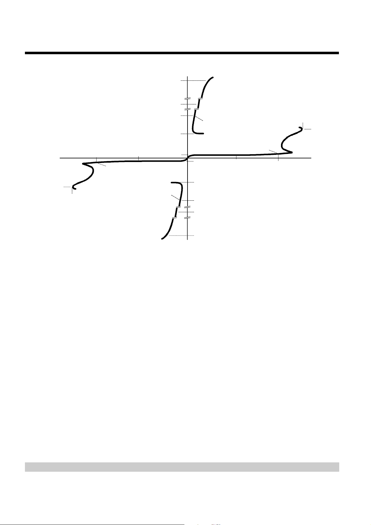
PARAMETER MEASUREMENT INFORMATION
-v
I
(BO)
V
Quadrant III
Switching
Characteristic
(BO)
+i
I
TSP
Characteristic
I
TSM
I
T
V
T
I
H
I
V
DRM
I
DRM
V
D
I
D
I
D
I
H
V
T
I
T
I
TSM
I
TSP
V
D
DRM
-i
Quadrant I
Switching
V
DRM
V
(BO)
PMXXAAB
I
(BO)
+v
Figure 1. VOLTAGE-CURRENT CHARACTERISTIC FOR R AND T TERMINALS
ALL MEASUREMENTS ARE REFERENCED TO THE T TERMINAL
PRODUCT INFORMATION
4
Page 5

100
V
DRM
DERATING FACTOR
vs
MINIMUM AMBIENT T EM P ERATURE
T
AMIN
- Minimum Ambient Temperature - °C
-40 -35 -30 -25 -20 -15 -10 -5 0
Derating Factor
0.95
0.96
0.97
0.98
0.99
1.00
TC4XAB
'4125
THRU
'4180
'4072
AND
'4082
'4240
THRU
'4380
NORMALISED HOLDING CURRENT
vs
JUNCTION TEMPERATURE
TJ - Junction Temperature - °C
-25 0 25 50 75 100 125 150
Normalised Holding Current
0.4
0.5
0.6
0.7
0.8
0.9
1.5
2.0
1.0
TC4XAD
10
TISP4072F3LM, TISP4082F3LM, TISP4125F3LM, TISP4150F3LM, TISP4180F3LM
TISP4240F3LM, TISP4260F3LM, TISP4290F3LM, TISP4320F3LM, TISP4380F3LM
BIDIRECTIONAL THYRISTOR OVERVOLTAGE PROTECTORS
DECEMBER 1998 - REVISED APRIL 1999
TYPICAL CHARACTERISTICS
OFF-STATE CURRENT
vs
JUNCTION TEMPERATURE
TC4XAA
1
0·1
- Off-State Current - µA
D
I
0·01
0·001
-25 0 25 50 75 10 0 125 150
TJ - Junction Temperature - °C
VD = 50 V
Figure 2. Figure 3.
NORMALISED V
ON-STATE CURRENT
vs
vs
ON-STATE VOLTAGE
100
1.1
10
1.0
PRODUCT INFORMATION
- On-State Current - A
Normalised to 25°C Value
T
I
(BO)
V
1
0.9
AMBIENT TEMPERATURE
'4240
THRU
'4380
'4072
150°C
AND
'4082
-25 0 25 50 75 100 125 150
23456789110
VT - On-State Voltage - V
TA - Ambient Temperature - °C
25°C
-40°C
Figure 4. Figure 5.
(BO)
'4125
THRU
'4180
VD = -50 V
TC3MAL
TC4XAC
'4072
AND
'4082
'4240
THRU
'4380
5
Page 6

TISP4072F3LM, TISP4082F3LM, TISP4125F3LM, TISP4150F3LM, TISP4180F3LM
TISP4240F3LM, TISP4260F3LM, TISP4290F3LM, TISP4320F3LM, TISP4380F3LM
BIDIRECTIONAL THYRISTOR OVERVOLTAGE PROTECTORS
DECEMBER 1998 - REVISED APRIL 1999
TYPICAL CHARACTERISTICS
NORMALISED BREAKOVE R V O LTAGE
vs
RATE OF RIS E OF PRINCIPAL CURRENT
1.3
POSITIVE POLARITY
1.2
'4240
THRU
'4380
1.1
Normalised Breakover Voltage
1.0
0·001 0·01 0·1 1 10 100
di/dt - Rate of Rise of Principal Current - A/µ s
TC4XAE
'4072
AND
'4082
'4125
THRU
'4180
Figure 6. Figure 7.
NORMALISED BREAKOVER VOLTAGE
vs
RATE OF RI SE O F PRINCIPAL CURRE NT
1.3
NEGATIVE POLARITY
'4125
1.2
1.1
Normalised Breakover Voltage
1.0
0·001 0·01 0·1 1 10 100
di/dt - Rate of Rise of Principal Current - A/µs
THRU
'4180
'4240
THRU
'4380
TC4XAF
'4072
AND
'4082
OFF-ST ATE CAPACITANCE
vs
TERMINAL VOLTAGE
100
90
80
70
60
50
40
30
20
Off-State Capa c i tance - pF
10
0·1 1 10
Terminal Voltage - V
POSITIVE PO LARITY
Figure 8. Figure 9.
'4125
THRU
'4180
TC4XAG
'4072
AND
'4082
'4240
THRU
'4380
50
OFF-S TATE CAPACI T ANCE
vs
TERMINAL VOLTAG E
100
90
80
70
60
50
40
30
20
Off-State Capacitance - pF
10
0·1 1 10
Terminal Voltage - V
NEGATIVE PO LARITY
'4125
THRU
'4180
TC4XAH
'4072
AND
'4082
'4240
THRU
'4380
50
PRODUCT INFORMATION
6
Page 7

TISP4072F3LM, TISP4082F3LM, TISP4125F3LM, TISP4150F3LM, TISP4180F3LM
TISP4240F3LM, TISP4260F3LM, TISP4290F3LM, TISP4320F3LM, TISP4380F3LM
BIDIRECTIONAL THYRISTOR OVERVOLTAGE PROTECTORS
DECEMBER 1998 - REVISED APRIL 1999
THERMAL INFORMATION
NON-REPETITIVE PEAK ON-STATE CURRENT
vs
10
CURRENT DURATION
9
8
7
6
5
4
3
2
V
= 600 Vrms, 50/60 Hz
GEN
= 1.4*V
R
GEN(t)
GEN
/ I
TI4LAAA
TSM(t)
device symbolization code
Devices will be coded as below.
- Non-Repetitive Peak On-State Current - A
TSM(t)
I
1
0·1 1 10 100 1000
t - Current Duration - s
Figure 10.
MECHANICAL DATA
DEVICE
TISP4072F3 4072F3
TISP4082F3 4082F3
TISP4125F3 4125F3
TISP4150F3 4150F3
TISP4180F3 4180F3
TISP4240F3 4240F3
TISP4260F3 4260F3
TISP4290F3 4290F3
TISP4320F3 4320F3
TISP4380F3 4380F3
SYMOBLIZATION
CODE
carrier information
Devices are shipped in one of the carriers below. A reel contains 2 000 devices.
PACKAGE TYPE CARRIER ORDER #
Straight Lead DO-92 Bulk Pack TISP4xxxF3LM
Straight Lead DO-92 Tape and Reeled TISP4xxxF3LMR
Formed Lead DO-92 Tape and Reeled TISP4xxxF3LMFR
PRODUCT INFORMATION
7
Page 8

TISP4072F3LM, TISP4082F3LM, TISP4125F3LM, TISP4150F3LM, TISP4180F3LM
TISP4240F3LM, TISP4260F3LM, TISP4290F3LM, TISP4320F3LM, TISP4380F3LM
BIDIRECTIONAL THYRISTOR OVERVOLTAGE PROTECTORS
DECEMBER 1998 - REVISED APRIL 1999
MECHANICAL DATA
LM002 (DO-92)
2-pin cylindrical plastic package
This single-in-lin e package consists of a circui t mounted on a lead frame an d encapsulated with in a plastic
compound. The compound will withstand soldering temperature with no deformation, and circuit performance
characteristics will remain stable when operated in high humidity conditions. Leads require no additional
cleaning or processing when used in soldered assembly. .
LM002 Package (DO- 92)
5,21
4,44
3,43 MIN.
2,67
2,03
2,20 MAX.
0,56
0,40
1,40
1,14
2
1 3
5,34
4,32
12,7 MIN.
4,19
3,17
2,67
2,03
A
0,41
0,35
2
3 1
VIEW A
2,67
2,41
ALL LINEAR DIMENSIONS IN MILLIMETERS
PRODUCT INFORMATION
8
MD4XARA
Page 9

TISP4072F3LM, TISP4082F3LM, TISP4125F3LM, TISP4150F3LM, TISP4180F3LM
TISP4240F3LM, TISP4260F3LM, TISP4290F3LM, TISP4320F3LM, TISP4380F3LM
BIDIRECTIONAL THYRISTOR OVERVOLTAGE PROTECTORS
DECEMBER 1998 - REVISED APRIL 1999
MECHANICAL DATA
LM002 (DO-92) - Formed Leads V ersion
2-pin cylindrical plastic package
This single-in-line package c onsists of a circuit mounted on a lead frame and encapsulated withi n a plastic
compound. The compound will withstand soldering temperature with no deformation, and circuit performance
characteristics will remain stable when operated in high humidity conditions. Leads require no additional
cleaning or processing when used in soldered assembly.
LMF002 (DO-92) - Formed Leads Version of LM002
5,21
4,44
3,43 MIN.
2,67
2,03
2,20 MAX.
0,56
0,40
2,90
2,40
2
1 3
5,34
4,32
4,00 MAX.
2,90
2,40
4,19
3,17
2,67
2,03
A
3 1
0,41
0,35
2
VIEW A
ALL LINEAR DIMENSIONS IN MILLIMETERS
PRODUCT INFORMATION
MD4XASA
9
Page 10

TISP4072F3LM, TISP4082F3LM, TISP4125F3LM, TISP4150F3LM, TISP4180F3LM
TISP4240F3LM, TISP4260F3LM, TISP4290F3LM, TISP4320F3LM, TISP4380F3LM
BIDIRECTIONAL THYRISTOR OVERVOLTAGE PROTECTORS
DECEMBER 1998 - REVISED APRIL 1999
MECHANICAL DATA
tape dimensions
LM002 Package (Straight Lead DO-92) Tape LM002 Tape Dimensions Conform to
13,70
11,70
32,00
23,00
27,68
17,66
11,00
8,50
Adhesive Tape on Reverse
Side - Shown Dashed
2,50 MIN.
3,14
2,14
VIEW A
5,48
4,68
13,00
12,40
the Requirements of EIA-468-B
Body Indent Visible
0,50
0,00
9,75
8,50
19,00
5,50
φφφφ
19,00
17,50
4,30
3,70
Flat of DO-92 Body
Towards Reel Axis
Tape Section
Shown in
View A
Direction of Feed
ALL LINEAR DIMENSIONS IN MILLIMETERS
MD4XAPC
PRODUCT INFORMATION
10
Page 11

TISP4072F3LM, TISP4082F3LM, TISP4125F3LM, TISP4150F3LM, TISP4180F3LM
TISP4240F3LM, TISP4260F3LM, TISP4290F3LM, TISP4320F3LM, TISP4380F3LM
tape dimensions
BIDIRECTIONAL THYRISTOR OVERVOLTAGE PROTECTORS
DECEMBER 1998 - REVISED APRIL 1999
MECHANICAL DATA
LMF002 Package (Formed Lead DO-92) Tape LMF002 Tape Dimensions Conform to
13,70
11,70
32,00
23,00
27,68
17,66
Adhesive Tape on Reverse
16,53
15,50
Side - Shown Dashed
11,00
8,50
2,50 MIN.
5,28
4,88
4,21
3,41
13,00
12,40
the Requirements of EIA-468-B
9,75
8,50
VIEW A
Body Indent Visible
0,50
0,00
19,00
5,50
φφφφ
19,00
17,50
4,30
3,70
Flat of DO-92 Body
Towards Reel Axis
Tape Section
Shown in
View A
Direction of Feed
ALL LINEAR DIMENSIONS IN MILLIMETERS
MD4XAQC
PRODUCT INFORMATION
11
Page 12

TISP4072F3LM, TISP4082F3LM, TISP4125F3LM, TISP4150F3LM, TISP4180F3LM
TISP4240F3LM, TISP4260F3LM, TISP4290F3LM, TISP4320F3LM, TISP4380F3LM
BIDIRECTIONAL THYRISTOR OVERVOLTAGE PROTECTORS
DECEMBER 1998 - REVISED APRIL 1999
IMPORTANT NOTICE
Power Innovations Limited (PI) re se rves the r ig ht t o make chan g es t o it s pr od uc ts o r t o di sc ont inu e any s em ic o nduc t or p r o duct
or service without notice, and advises its customers to verify, before placing orders, that the information being relied on is
current.
PI warrants performance of its semiconductor products to the specifications applicable at the time of sale in accordance with
PI's standard w arr anty. Testing and other quality cont rol tec hn iqu es are uti li z ed to the exten t PI deems necessary to support this
warranty. Specific testing of all parameters of each device is not necessarily performed, except those mandated by government
requirements.
PI assumes no liability for applications assistance, customer product design, software performance, or infringement of patents
or services described herein. Nor is any license, either express or implied, granted under any patent right, copyright, design
right, or other intellectual property right of PI covering or relating to any combination, machine, or process in which such
semiconductor products or services might be or are used.
PI SEMICONDUCTOR PRODUCTS ARE NOT DESIGNED, INTENDED, AUTHORISED, OR WARRANTED TO BE SUITABLE
FOR USE IN LIFE-SUPPORT APPLICATIONS, DEVICES OR SYSTEMS.
Copyright © 1999, Power Innovations Limited
PRODUCT INFORMATION
12
 Loading...