

Page 1

THBT7011D
ApplicationSpecific Discretes
A.S.D.
FEATURES
BIDIRECTIONALCROWBARPROTECTION.
PEAKPULSECURRENT:
=30Afor 10/1000µs surge.
I
PP
HOLDINGCURRENT:
I
= 150mA.
H
BREAKDOWNVOLTAGE:70VMin.
LOW DYNAMICBREAKOVERVOLTAGE.
DESCRIPTION
Dedicated to telecommunication equipment
protection,thisdeviceprovidesa dualbidirectional
protectionfunction.
Dynamic characteristics have been defined for
severaltypesof surges,in order to meet the SLIC
maximumratings.
DUAL OVERVOLTAGE
PROTECTION FOR TELECOM LINE
SO-8
FUNCTIONAL DIAGRAM
T
R
TM: ASD is trademarksof STMicroelectronics.
January 1999 - Ed: 5C
G
PINOUTCONFIGURATION
T
NC
NC
R
G
G
G
G
1/8
Page 2
THBT7011D
COMPLIESWITH THE
FOLLOWING STANDARDS:
Peak Surge
Voltage
(V)
Voltage
Waveform
(µs)
Current
Waveform
(µs)
Admissible
Ipp
(A)
Necessary
Resistor
(Ω)
CCITTK20 4000 10/700 5/310 25 VDE0433 4000 10/700 5/310 40 10
VDE0878 4000 1.2/50 1/20 50 IEC-1000-4-5
FCCPart68, lightningsurge
typeA
FCCPart68, lightningsurge
level4
level4
1500
800
10/700
1.2/50
10/160
10/560
5/310
8/20
10/160
10/560
25
50
47
35
100 9/720 5/320 25 -
15.5
typeB
BELLCORETR-NWT-001089
Firstlevel
BELLCORETR-NWT-001089
2500
1000
2/10
10/1000
2/10
10/1000
90
30
5000 2/10 2/10 90 50
Secondlevel
CNETl31-24
ABSOLUTE MAXIMUM RATINGS
4000 0.5/700 0.8/310 25 -
=25°C)
(T
amb
Symbol Parameter Value Unit
-
-
25
23
24
I
PP
I
TSM
Peak pulsecurrent (seenote1) 10/1000µs30 A
Non repetitivesurge peak on-statecurrent
(F=50Hz)
T
stg
T
j
T
L
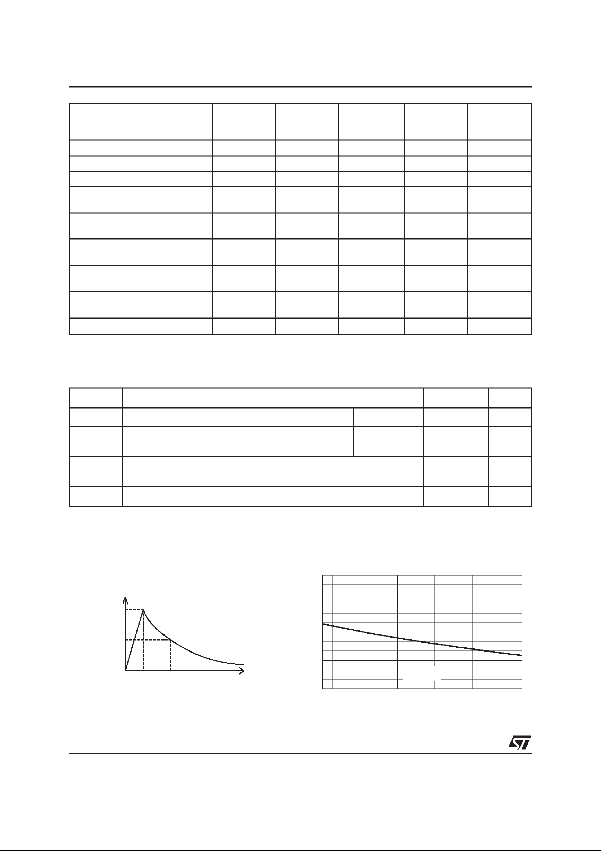
Note 1 : Pulsewaveform :
Storagetemperaturerange
Maximumoperatingjunctiontemperature
Maximumleadtemperature forsolderingduring 10s 260 °C
10/1000µst
%I
100
50
0
=10µst
r
PP
t
r
tp = 100ms
t=1s
=1000µs
p
t
p
t
Itsm ( A )
30
25
20
15
10
5
0
50 100 200 500 1 000 2 000
t ( ms )
15.5
9
- 40 to+ 150
+ 150
A
°C
°C
F=50Hz
Tj initial=+25°C
2/8
Page 3

THBT7011D
TESTCIRCUITS FORI
PP
Transversal mode
See test
circuit 3
TIP or
RING
I
PP
R
P
THBT
GND
THERMAL RESISTANCES
Symbol Parameter Value Unit
R
th (j-a)
ELECTRICALCHARACTERISTICS
Symbol Parameter
V
RM
I
RM
V
R
V
BR
V
BO
I
H
I
BO
I
PP
C Capacitance
Junctionto ambient
=25°C)
(T
amb
Stand-offvoltage
Leakagecurrent at stand-offvoltage
ContinuousReversevoltage
Breakdownvoltage
Breakovervoltage
Holdingcurrent
Breakovercurrent
Peakpulse current
170 °C/W
I
I
PP
I
BO
I
H
I
R
V
VRMV
R
BR
V
V
BO
STATICPARAMETERS BETWEENTIPAND GND,RINGANDGND
Type I
max. max.
@V
RM
AV
µ
RM
IR@V
R
note1
AV VmAmAmApF
µ
VBO@I
max.
note2
BO
I
H
min. max. min
note 3
THBT7011D 5 66 50 70 89 50 400 150 80
C
max
note4
3/8
Page 4

THBT7011D
STATICPARAMETERSBETWEENTIPANDRING
Type I
RM
@V
RM
IR@V
R
max. note6 max. note 6 max
AV
µ
AVpF
µ
THBT7011D 5 132 50 140 40
Note 1: IRmeasured at VRguarantees VBR>V
Note 2: Measured at50 Hz (1cycle) testcircuit 1.
Note 3: See the reference testcircuit 2.
Note 4: V
Note 5: See testcircuit 3for V
Note 6: Ground notconnected or |V
= 1V,F =1MHz.
R
dynamic parameters;Rpis theprotection resistorlocated on the line card.
BO
TIP
|=|V
R
| versusGround
RING
DYNAMICBREAKOVERVOLTAGES(Transversalmode)
Type Symbol Testconditions (seenote5) Maximum Unit
THBT7011D V
BO
10/700µs 1.5kV Rp=10Ω IPP=30A
1.2/50µs 1.5kV R
2/10µs 2.5kV R
=10Ω IPP=30A
p
=62Ω IPP=38A
p
90
95
150
TESTCIRCUIT 1 for IBOandVBOparameters:
C
note4
V
tp
Auto
Transfo rmer
220V/2A
static
relay.
V
out
220V
Transf or m er
220V/800V
5A
measure
TESTPROCEDURE:
PulseTestduration(tp = 20ms):
- For Bidirectionaldevices= SwitchKis closed
- For Unidirectionaldevices= SwitchK isopen.
V
Selection
OUT
- Devicewith V
-V
- DevicewithV
-V
BO
OUT
OUT
< 200Volt
= 250V
≥ 200 Volt
BO
= 480V
RMS,R1
RMS,R2
=140Ω.
= 240 Ω.
=20ms
K
I
BO
R1
140
R2
240
D.U.T
V
BO
measure
4/8
Page 5

TESTCIRCUIT 2 for IHparameter.
V
= - 48 V
BAT
Thisisa GO-NOGOtestwhichallowsto confirmtheholding current(IH) level in a functional
testcircuit.
TESTPROCEDURE :
R
D.U.T .
THBT7011D
-V
P
Surge generator
1) Adjustthecurrentlevel at theI
valuebyshortcircuitingtheAKofthe D.U.T.
H
2) Firethe D.U.Twitha surgeCurrent: Ipp = 10A , 10/1000µs.
3) TheD.U.Twill comebackoff-state within 50msmax.
TESTCIRCUIT 3 for I
(V is defined in no load condition)P
and VBOparameters:
PP
L
R
R
4
TIP
2
RING
R
3
V
CC
P
1
R
1
2
GND
Pulse(µs) V
t
r
t
p
p
(V) (µF) (nF) (µH) (Ω)(Ω)(Ω)(Ω) (A) (Ω)
C
1
C
2
LR
1
R
2
R
3
R
4
IPPR
10 700 1500 20 200 0 50 15 25 25 30 10
1.2 50 1500 1 33 0 76 13 25 25 30 10
2 10 2500 10 0 1.1 1.3 0 3 3 38 62
p
5/8
Page 6

THBT7011D
APPLICATIONCIRCUIT :
1 - Line card protection
RING
GENERA T OR
-V
BAT
LINE A
LINE B
PTC
T
E
S
T
R
E
L
A
Y
S
THBT7011D
PTC
RING
RELAY
LCP1511D
220
SLIC
nF
6/8
Page 7

ORDERCODE
THBT 70 1 1 D RL
BIDIRECTIONAL
TRISIL
BREAKDOWN
VOLTAGE
MARKING
Types Package Marking
THBT7011D SO-8 BT701D
VERSION
THBT7011D
PACKAGING:
RL = tapeandreel.
= tube.
LOW DYNAMIC
CHARACTERISTICS.
PACKAGE:
1=SO8Plastic.
PACKAGEMECHANICAL DATA.
SO-8 Plastic
L
A
a2
b
8
1
e
e3
D
M
5
4
S
F
c1
C
a
1
E
Packaging : Productssupplied in antistatictubes
or tape andreel.
Weight:
0.08g
a3
b
1
MARKING :
Logo, DateCode, PartNumber.
REF. DIMENSIONS
Millimetres Inches
Min. Typ. Max. Min. Typ. Max.
A 1.75 0.069
a1 0.1 0.25 0.004 0.010
a2 1.65 0.065
a3 0.65 0.85 0.025 0.033
b 0.35 0.48 0.014 0.019
b1 0.19 0.25 0.007 0.010
C 0.25 0.50 0.50 0.010 0.020
c1 45°(typ)
D 4.8 5.0 0.189 0.197
E 5.8 6.2 0.228 0.244
e 1.27 0.050
e3 3.81 0.150
F 3.8 4.0 0.15 0.157
L 0.4 1.27 0.016 0.050
M 0.6 0.024
S8°(max)
7/8
Page 8

THBT7011D
Informationfurnished is believedto be accurateand reliable. However, STMicroelectronics assumes no responsIbility for the consequencesof
use ofsuch informationnor forany infringementof patentsor other rights of thirdparties which mayresult from its use.Nolicense isgranted by
implication or otherwise under any patent or patent rights of STMicroelectronics. Specifications mentioned in this publication are subject to
change withoutnotice. This publicationsupersedes and replaces all informationpreviously supplied.
STMicroelectronics products are not authorized for use as critical components in life support devices or systems withoutexpress written approval ofSTMicroelectronics.
The ST logo is a registeredtrademark of STMicroelectronics
1998STMicroelectronics - Printed in Italy - All rightsreserved.
STMicroelectronics GROUP OF COMPANIES
Australia - Brazil - Canada - China - France - Germany - Italy - Japan - Korea - Malaysia - Malta - Mexico - Morocco -
The Netherlands - Singapore - Spain -Sweden - Switzerland - Taiwan - Thailand -United Kingdom - U.S.A.
http://www.st.com
8/8
 Loading...