

Page 1
THBT200S
ApplicationSpecific Discretes
A.S.D.
FEATURES
DUALBIDIRECTION ALCROWBARPROTECTION.
PEAK PULSECURRENT :
-I
= 75 A, 10/1000 µs.
PP
HOLDINGCURRENT = 150 mA min
BREAKDOWNVOLTAGE=200Vmin.
BREAKOVERVOLTAGE= 290V max.
MONOLITHICDEVICE.
DESCRIPTION
This monolithic protection device has been especiallydesignedto protectsubscriberline cards.The
THBT200 device is particularly suitable to protect
ring generator relay against transient overvoltages.
TRANSIENT VOLTAGE SUPPRESSOR
FOR SLIC PROTECTION
SIP3
COMPLIESWITHTHE FOLLOWINGSTANDARDS:
CCITTK20:
10/700µs 1kV
5/310µs 25A
VDE0433: 10/700µs 2kV
µs 50A
5/310
VDE0878: 1.2/50
µs 1.5kV
1/20 µs 40A
FCCpart68 : 2/10 µs 2.5kV
2/20µs 225A(*)
BELLCORE
TR-NWT-001089: 2/10 µs 2.5kV
2/10µs 225A(*)
10/1000µs 1kV
10/1000µs 75A(*)
(*)with series resistorsor PTC.
TM: ASDis trademarks of SGS-THOMSON Microelectronics.
February 1998 Ed:2
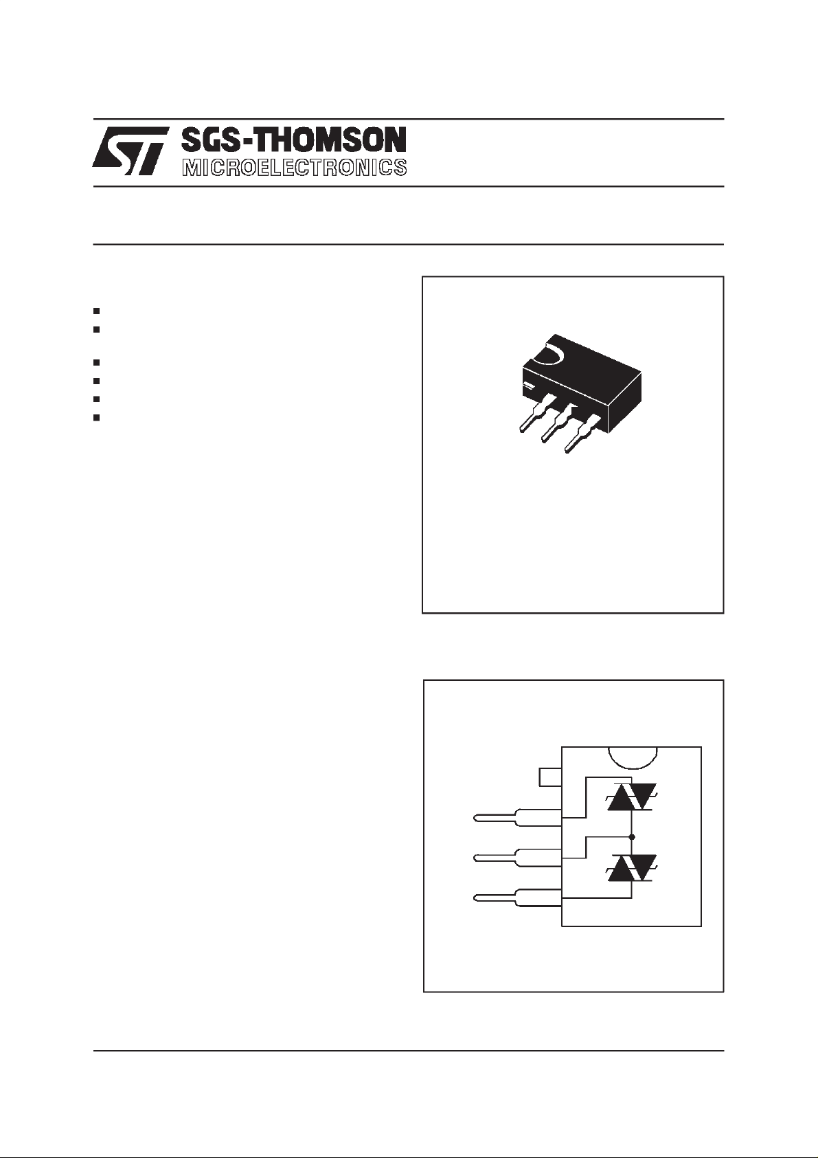
SCHEMATICDIAGRAM
NC
Tip
GND
Ring
1
2
3
4
1/7
Page 2
THBT200S
ABSOLUTE MAXIMUM RATINGS(T
amb
=25°C)
Symbol Parameter Value Unit
I
PP
I
TSM
Peakpulse current(see note 1) 10/1000 µs
µs
5/310
µs
8/20
2/10
µs
Nonrepetitivesurge peak on-statecurrent
tp= 20ms 30 A
75
125
150
225
(F= 50Hz)
T
T
T
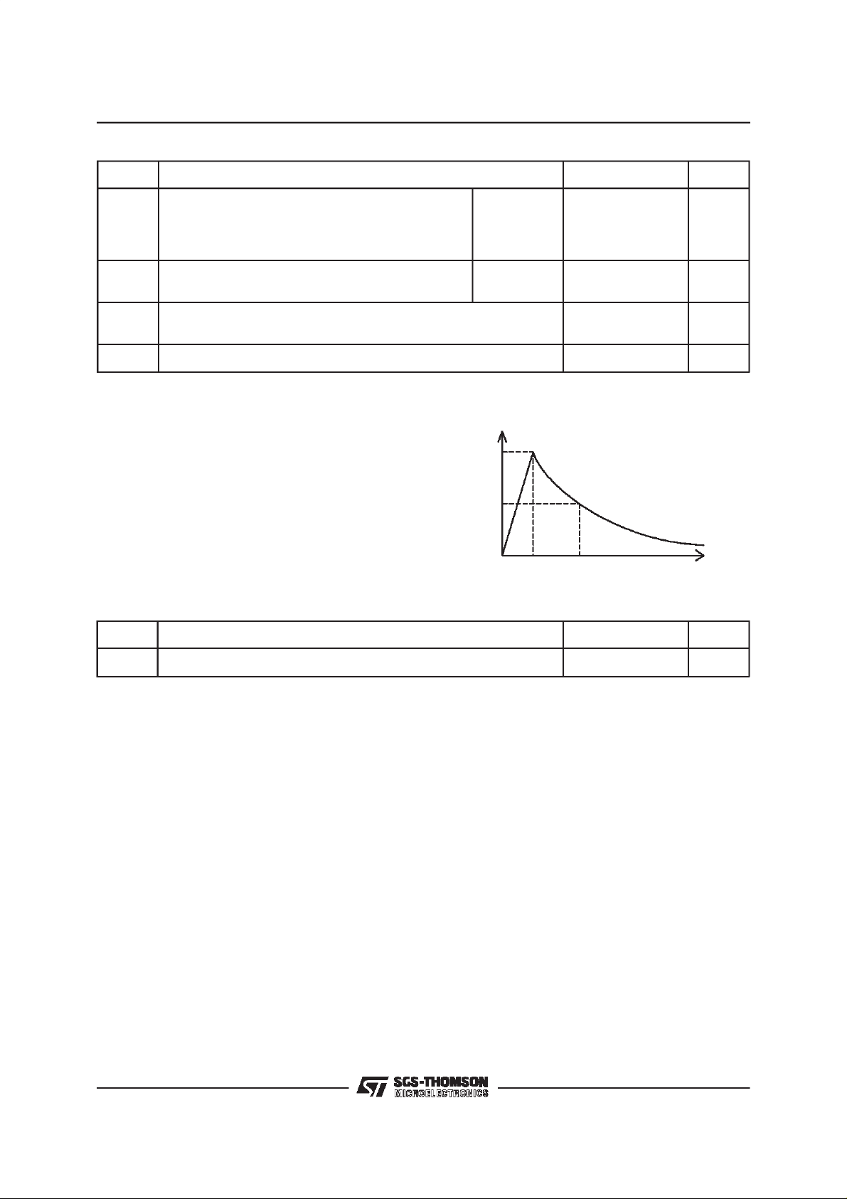
Note 1: Pulse waveform:
Storagetemperaturerange
stg
Maximumjunction temperature
j
Maximumlead temperatureforsolderingduring 10s 230 °C
L
10/1000µstr=10µst
5/310µst
2/10µst
=1000µs
=5µst
r
=2µst
r
p
=310µs
p
=10µs
p
%I
100
50
0
PP
t
rp
- 40 to + 150
150
t
°C
A
t
THERMAL RESISTANCE
Symbol Parameter Value Unit
R
th (j-a)
Junctionto ambient 80 °C/W
2/7
Page 3

THBT200S
ELECTRICALCHARACTERISTICS
Symbol Parameter
V
I
RM
V
V
I
I
BO
I
PP
Stand-offvoltage
RM
Leakagecurrent at V
Continuousreversevoltage
BR
Breakovervoltage
BO
Holdingcurrent
H
Breakovercurrent
Peakpulse current
RM
(T
amb
=25°C).
I
I
pp
I
BO
I
H
I
RM
V
RMVBR
C Capacitance
PARAMETERS RELATEDTO ONE TRISIL(BetweenTIPandGNDorRINGand GND)
@V
I
RM
RM
VBR@I
R
V
BO @IBO
I
H
V
V
BO
C
max. min. max. min. max. min. max.
note1 note2 note 3
A V V mA V mA mA mA pF
µ
10 180 200 1 290 150 800 150 200
Note 1: See referencetest circuit 1 for IBOandVBOparameters.
Note 2: See testcircuit 2.
Note 3:VR=1V, F =1MHz.
3/7
Page 4

THBT200S
REFERENCETESTCIRCUIT 1 FORIBOandVBOparameters:
t
TESTPROCEDURE:
PulseTestduration (tp = 20ms):
-ForBidirectionaldevices= SwitchK is closed
-ForUnidirectionaldevices= SwitchK is open.
V
Selection
OUT
-DevicewithV
-V
- Devicewith V
-V
BO
OUT
BO
OUT
< 200 Volt
=250V
≥ 200 Volt
=480V
RMS,R1
RMS,R2
=140Ω.
= 240Ω.
FUNCTIONALHOLDINGCURRENT(IH) TESTCIRCUIT2.
R
D.U.T.
V
= - 48 V
BAT
Thisisa GO-NOGOTestwhichallowsto confirmtheholdingcurrent (I
testcircuit.
TESTPROCEDURE :
1) Adjustthecurrentlevel at theI
2) Firethe D.U.Twitha surgeCurrent: Ipp = 10A , 10/1000µs.
3) TheD.U.Twill comebackoff-state within50msmax.
valueby short circuitingthe AKoftheD.U.T.
H
Surge generator
)levelina functional
H
-V
P
4/7
Page 5

APPLICATIONCIRCUIT
Typicalline cardprotection concept
RING
GENERATOR
-V
THBT200S
bat
LINE A
PTC
T
E
S
T
R
E
L
A
Y
S
LINE B
PTC
FUNCTIONAL DESCRIPTION
Line A
THBT200S
Tip
TIP
RING
RELAY
SLIC
RING
THDTxxx
or
LCPxxx
LINE A AND LINEB PROTECTION.
Each line (TIP and RING) is protected by a bidirectionalTrisil, which triggers at amaximumvoltage equal totheV
BO
.
Line B
Ring
5/7
Page 6

THBT200S
Fig. 1 : Relativevariationof holding currentversus
junctiontemperature.
Fig. 2
: Surgepeak current versus overload dura-
tion.
IH[Tj]
I
=25°C]
H[Tj
1.0
0.8
0.6
0.4
0.2
T
(°C)
j
0.0
0 20 40 60 80 100 120 140
Fig.3 : Peakonstatevoltageversuspeak on state
current(typicalvalues).
I (A)TSM
40
F=50Hz
Tj initial=25°C
30
20
10
0
1E-2 1E-1 1E+0 1E+1 1E+2 1E+3
t(s)
Fig. 4 : Capacitanceversus reverse applied volt-
age (typicalvalues).
1000
100
6/7
10
1 10 100 200
Page 7

ORDERCODE
BIDIRECTIONALTRISIL
BREAKDOWNVOLTAGE
MARKING :
Package Types Marking
SIP3 THBT200S THBT200S
THBT200S
THBT 200 S
PACKAGE:
S = SIP3
PACKAGEMECHANICAL DATA
SIP3 Plastic
B
I
a2
b1
Z
Packaging:
Weight:
0.55g
e
e
3
Productssuppliedin antistatictubes.
a1
L
b2
c1
REF. DIMENSIONS
Millimetres Inches
Min. Typ. Max. Min. Typ. Max.
A 7.10 0.280
a1 2.80 0.110
A
a2 1.50 1.90 0.059 0.075
B 10.15 0.400
b1 0.50 0.020
b2 1.35 1.75 0.053 0.069
c1 0.38 0.50 0.015 0.020
e 2.54 0.100
e3 7.62 0.200
I 10.50 0.413
L 3.30 0.130
Z 1.50 0.059
Information furnished is believed to be accurate and reliable.However, SGS-THOMSON Microelectronics assumes no responsibility for the
consequences of use of such information norfor any infringement ofpatentsor other rights of third parties which may resultfrom itsuse. No
license is grantedby implicationor otherwise underany patentor patentrights ofSGS-THOMSON Microelectronics.Specifications mentioned
in thispublication are subjectto changewithoutnotice. Thispublication supersedes andreplacesall informationpreviously supplied.
SGS-THOMSONMicroelectronics productsare notauthorized foruseas criticalcomponents inlife supportdevicesor systems withoutexpress
written approval of SGS-THOMSONMicroelectronics.
1998 SGS-THOMSON Microelectronics - Printed inItaly- Allrights reserved.
SGS-THOMSON Microelectronics GROUP OF COMPANIES
Australia - Brazil-Canada -China-France -Germany - Italy - Japan- Korea-Malaysia- Malta -Morocco
The Netherlands- Singapore - Spain- Sweden - Switzerland - Taiwan-Thailand- United Kingdom - U.S.A.
7/7
 Loading...