

Datasheet THBT27011D, THBT20011D, THBT16011D, THBT15011D Datasheet (SGS Thomson Microelectronics)
Page 1
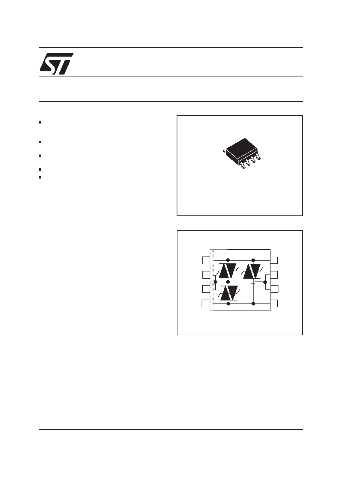
THBTxxx11D
ApplicationSpecific Discretes
A.S.D.
FEATURES
BIDIRECTIONALCROWBARPROTECTION
BETWEENTIP AND GND, RINGANDGND
ANDBETWEENTIP AND RING.
PEAKPULSECURRENT:
=30Afor 10/1000µs surge.
I
PP
HOLDINGCURRENT:
I
= 150mA.
H
AVAILABLEIN SO8 PACKAGES.
LOW DYNAMICBREAKOVERVOLTAGE.
DESCRIPTION
Dedicated to telecommunication equipment
protection, these devices provide a triple
bidirectionalprotection function.
They ensure the same protection capability with
the same breakdown voltage both in longitudinal
modeandtransversalmode.
A particularattentionhas beengiven to theinternal
wire bonding.The ”4-point”configurationensures
a reliable protection, eliminating overvoltages
introduced by the parasitic inductances of the
wiring (Ldi/dt), especially for very fast transient
overvoltages.
Dynamic characteristics have been defined for
several types of surges, in order to meetthe SLIC
maximumratings.
TRIPOLAR OVERVOLTAGE
PROTECTION FOR TELECOM LINE
SO8
SCHEMATIC DIAGRAM
TIP
GND
GND
1
2
3
8 TIP
GND
7
GND
6
COMPLIESWITHTHEFOLLOWINGSTANDARDS:
CCITTK20: 10/700µs 1.5kV
5/310µs 20A(*)
VDE0433:
VDE0878:
CNET: 0.5/700µs 1.5kV
FCCpart68 : 2/10µs 2.5kV
BELLCORE
TR-NWT-001089:
(*)With series resistors or PTC.
September 1998 - Ed: 5A
10/700µs 2kV
5/310µs 20A(*)
1.2/50µs 1.5kV
1/20µs 20A(*)
0.2/310µs 20A(*)
2/10µs 40A(*)
2/10µs 2.5kV
2/10µs 40A(*)
RING
TM: ASDis trademarks ofSGS-THOMSON Microelectronics.
4
5
RING
1/9
Page 2
THBTxxx11D
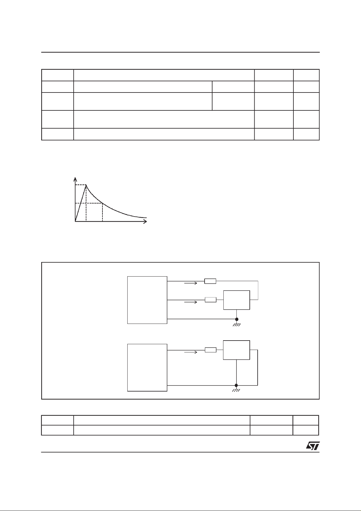
ABSOLUTE MAXIMUM RATINGS
(T
amb
=25°C)
Symbol Parameter Value Unit
I
PP
I
TSM
T
stg
T
j
T
L
Note 1 : Pulsewaveform :
Peak pulsecurrent (seenote 1) 10/1000µs30 A
Non repetitivesurge peak on-statecurrent
(F=50Hz)
Storagetemperaturerange
Maximumoperatingjunctiontemperature
tp= 10 ms
t=1s
8
3.5
- 40 to+ 150
+ 150
Maximumleadtemperature forsolderingduring 10s 260 °C
10/1000µst
%I
100
50
0
=10µst
r
PP
t
r
=1000µs
p
t
p
t
A
°C
°C
TESTCIRCUITS FORI
PP
Longitudinal mode
TIP
R
/2
I
See test
circuit 3
RING
PP
/2
I
PP
P
R
P
THBT
GND
Transversalmode
See test
circuit 3
TIP or
RING
I
PP
R
P
THBT
GND
THERMALRESISTANCES
Symbol Parameter Value Unit
R
th (j-a)
Junctionto ambient 170 °C/W
2/9
Page 3
THBTxxx11D
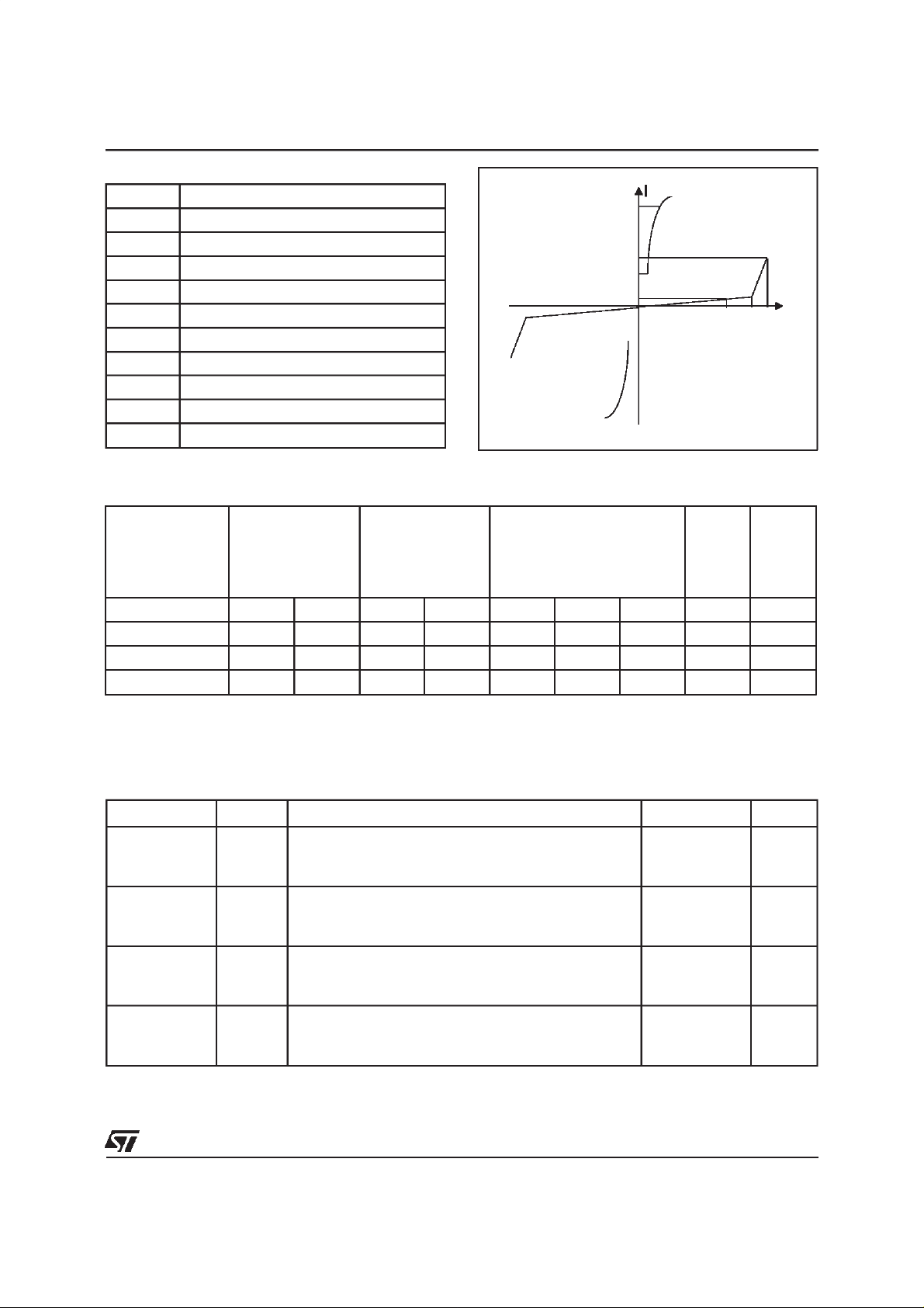
ELECTRICALCHARACTERISTICS(T
Symbol Parameter
V
RM
I
RM
V
V
BR
V
BO
I
H
I
BO
V
I
PP
Stand-offvoltage
Leakagecurrent at stand-offvoltage
ContinuousReverse voltage
R
Breakdownvoltage
Breakovervoltage
Holdingcurrent
Breakovercurrent
Forwardvoltagedrop
F
Peak pulsecurrent
amb
=25°C)
I
I
PP
I
BO
I
H
I
R
V
V
RM
BR
C Capacitance
STATICPARAMETERS
Type I
THBT15011D
@V
RM
RM
max. max.
µAVµA V V mAmAmA pF
IR@V
note1
R
VBO@I
max.
note 2
BO
I
H
min. max. min
note 3
note4
5 135 50 150 210 50 400 150 80
THBT16011D 5 135 50 160 230 50 400 150 80
THBT20011D 5 180 50 200 290 50 400 150 80
THBT27011D 5 240 50 270 380 50 400 150 80
Note 1: IRmesuared at VRguaranteesVBR>V
Note 2: Measured at 50Hz (1 cycle) test circuit1.
Note 3: See thereference test circuit 2.
Note 4: V
= 1V,F =1MHz.
R
R
V
V
BO
C
max
DYNAMICBREAKOVERVOLTAGES(Transversalmode)
Type Symbol Testconditions
THBT15011D V
BO
10/700µs 1.5kV Rp=10Ω IPP=30A
1.2/50µs 1.5kV R
2/10µs 2.5kV R
THBT16011D V
BO
10/700µs 1.5kV Rp=10Ω IPP=30A
1.2/50µs 1.5kV R
2/10µs 2.5kV R
THBT20011D V
BO
10/700µs 1.5kV Rp=10Ω IPP=30A
1.2/50µs 1.5kV R
2/10µs 2.5kV R
THBT27011D V
BO
10/700µs 1.5kV Rp=10Ω IPP=30A
1.2/50µs 1.5kV R
2/10µs 2.5kV R
Note 5: See test circuit 3 forVBOdynamic parameters; Rpisthe protectionresistor located on theline card.
(seenote5)
=10Ω IPP=30A
p
=62Ω IPP=38A
p
=10Ω IPP=30A
p
=62Ω IPP=38A
p
=10Ω IPP=30A
p
=62Ω IPP=38A
p
=10Ω IPP=30A
p
=62Ω IPP=38A
p
Maximum Unit
240
V
250
260
260
V
270
290
320
V
350
400
390
V
440
480
3/9
Page 4

THBTxxx11D
TESTCIRCUIT1 forIBOand VBOparameters:
Auto
Transformer
220V/2A
220V
Transfor mer
220V/800V
5A
TESTPROCEDURE:
PulseTestduration(tp = 20ms):
- For Bidirectionaldevices= SwitchK isclosed
- For Unidirectionaldevices= SwitchK isopen.
V
Selection
OUT
- DevicewithV
-V
- DevicewithV
-V
BO
OUT
OUT
< 200 Volt
= 250V
≥ 200 Volt
BO
= 480 V
V
out
RMS,R1
RMS,R2
static
relay.
= 140Ω.
=240Ω.
= 20ms
tp
K
I
BO
measure
R1
140
R2
240
D.U.T
V
BO
measure
TESTCIRCUIT2 forI
V
= - 48 V
BAT
This is a GO-NOGOtest whichallowsto confirmthe holdingcurrent (IH) level in a functional
test circuit.
TESTPROCEDURE:
1) Adjustthe currentlevel at the I
2) Fire theD.U.Twitha surgeCurrent: Ipp= 10A, 10/1000 µs.
3) The D.U.Twill comebackoff-state within50 msmax.
parameter.
H
R
D.U.T .
valueby shortcircuitingtheAKof the D.U.T.
H
-V
P
Surge generator
4/9
Page 5
THBTxxx11D
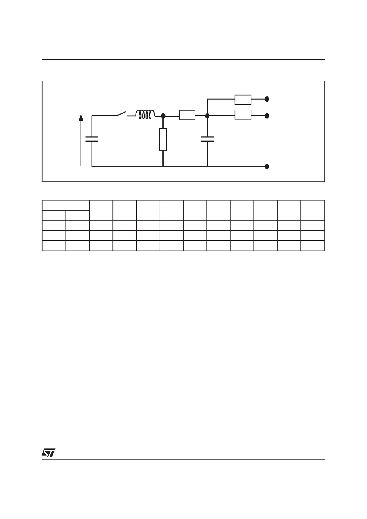
TESTCIRCUIT 3 for I
(V is defined in no loadcondition)P
and VBOparameters:
PP
L
R
R
4
TIP
2
RING
R
3
V
CC
P
1
R
1
2
GND
Pulse(µs) V
t
r
t
p
p
(V) (µF) (nF) (µH) (Ω)(Ω)(Ω)(Ω) (A) (Ω)
C
1
C
2
LR
1
R
2
R
3
R
4
IPPR
10 700 1500 20 200 0 50 15 25 25 30 10
1.2 50 1500 1 33 0 76 13 25 25 30 10
2 10 2500 10 0 1.1 1.3 0 3 3 38 62
p
5/9
Page 6
THBTxxx11D
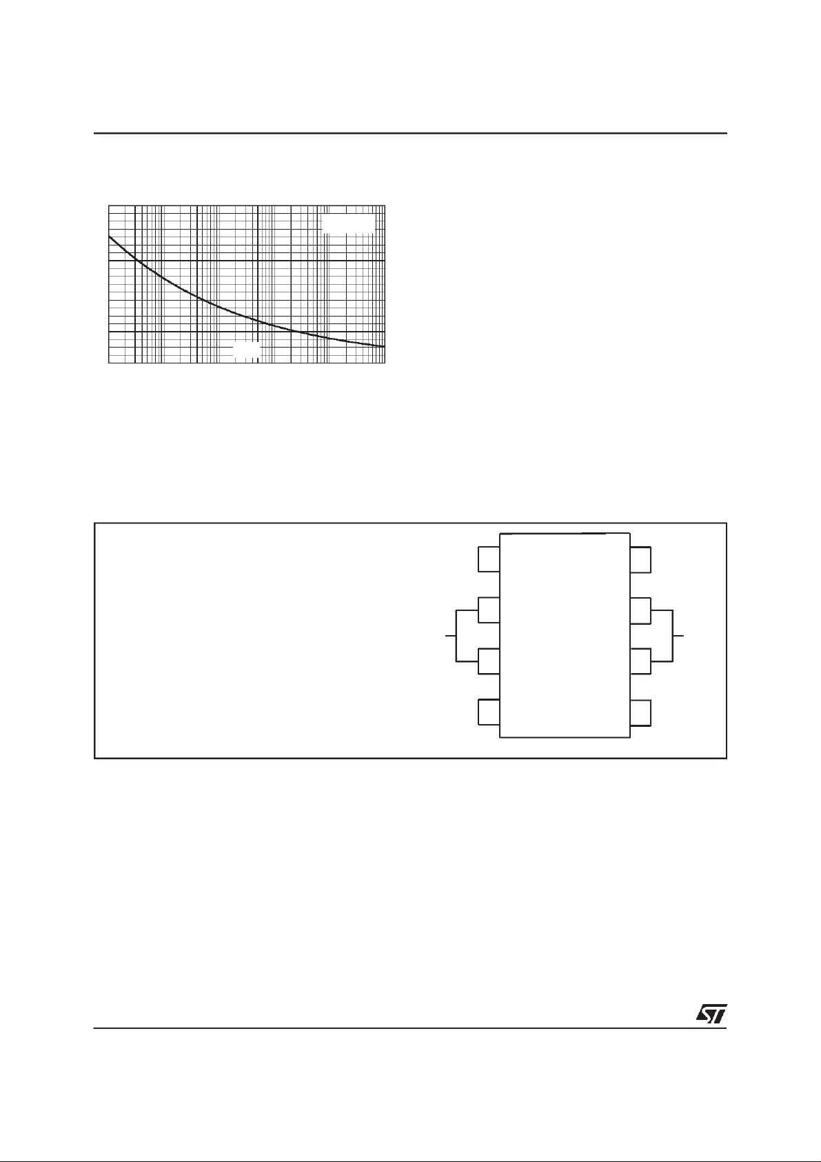
Fig. 1:
Surge peak current versus overload dura-
tion.
I (A)TSM
10
9
8
7
6
5
4
3
2
1
0
1E-2 1E-1 1E+0 1E+1 1E+2 1E+3
t(s)
F=50Hz
Tjinitial=25°C
APPLICATIONNOTE
1
Connectpins 2, 3,6 and 7 to Groundin
orderto guaranteea good surgecurrent
capabilityforlongduration disturbances.
TIP
1
8
TIP
2 In orderto take advantageofthe”4-point ”
structureof theTHBT, the TIP and RING
lineshave tocrossthedevice.In thiscase,
the devicewilleliminate the overvoltages
generatedby theparasiticinductancesof
the wiring(Ldi/dt),especially forveryfast
transients.
GND
RING
2
7
GND
3
4
6
5
RING
6/9
Page 7

APPLICATIONCIRCUIT :
1 - Line card protection
RING
GENERATOR
THBTxxx11D
-V
BA T
LINE A
LINE B
T
E
S
T
R
E
L
A
Y
S
PTC
RING
RELAY
THBTxxxD
PTC
2 - Protectionfor telephoneset withgroundkey
LA
LCP1511D
OOK
H
220
nF
PEECH
S
IALING
D
SLIC
LB
E
THBTxxxD
ROUND KEY
G
RINGER
7/9
Page 8
THBTxxx11D
ORDERCODE
BIDIRECTIONAL
TRISIL
THBT 150 1 1 D RL
PACKAGING:
RL = tapeandreel.
=tube.
LOWDYNAMIC
CHARACTERISTICS.
BREAKDOWN
VOLTAGE
MARKING
Types Package Marking
THBT15011D SO8 BT151D
THBT16011D SO8 BT161D
THBT20011D SO8 BT201D
THBT27011D SO8 BT271D
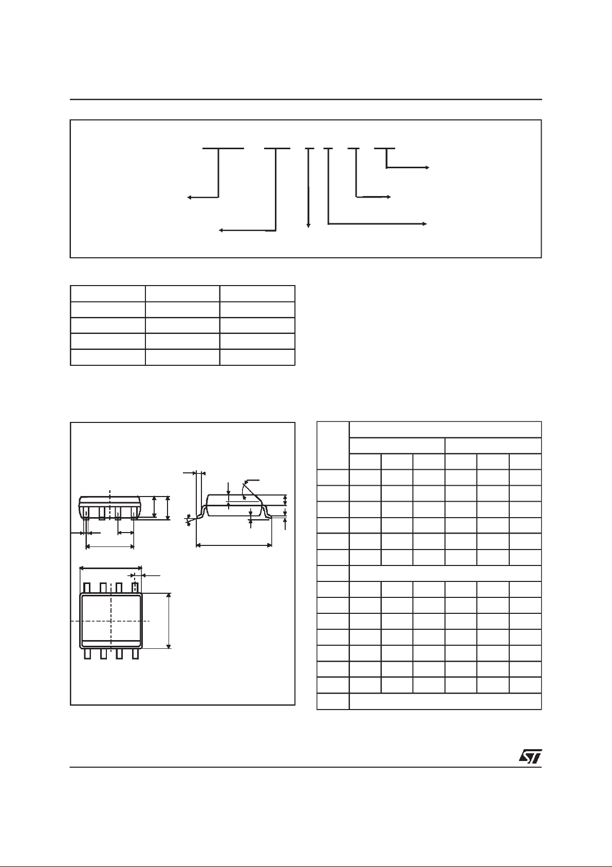
PACKAGEMECHANICAL DATA.
SO8 Plastic
L
A
a2
b
8
1
e
e3
D
M
5
4
S
F
c1
C
a
1
E
Packaging : Productssupplied in antistatic tubes
or tape andreel.
VERSION
MARKING :
REF. DIMENSIONS
A 1.75 0.069
a3
a1 0.1 0.25 0.004 0.010
a2 1.65 0.065
b
1
b 0.35 0.48 0.014 0.019
b1 0.19 0.25 0.007 0.010
C 0.50 0.020
c1 45°(typ)
D 4.8 5.0 0.189 0.197
E 5.8 6.2 0.228 0.244
e 1.27 0.050
e3 3.81 0.150
F 3.8 4.0 0.15 0.157
L 0.4 1.27 0.016 0.050
M 0.6 0.024
S8°(max)
PACKAGE:
1 = SO8Plastic.
Logo, DateCode, Part Number.
Millimetres Inches
Min. Typ. Max. Min. Typ. Max.
Weight:
8/9
0.077g
Page 9

THBTxxx11D
Informationfurnished is believedto be accurateand reliable. However, STMicroelectronics assumes no responsIbility for the consequencesof
use ofsuch informationnor forany infringementof patentsor other rights of thirdparties which mayresult fromits use.No license isgrantedby
implication or otherwise under any patent or patent rights of STMicroelectronics. Specifications mentioned in this publication are subject to
change withoutnotice. This publicationsupersedes and replaces all informationpreviously supplied.
STMicroelectronics products are not authorized for use as critical components in life support devices or systems without express written
approval ofSTMicroelectronics.
The ST logo is a registeredtrademark of STMicroelectronics
1998STMicroelectronics - Printed in Italy - Allrights reserved.
STMicroelectronics GROUP OF COMPANIES
Australia -Brazil - Canada - China - France - Germany - Italy - Japan - Korea - Malaysia -Malta - Mexico - Morocco -
The Netherlands Singapore -Spain - Sweden - Switzerland - Taiwan - Thailand - United Kingdom - U.S.A.
9/9
 Loading...