

Page 1
VISHAY
18088
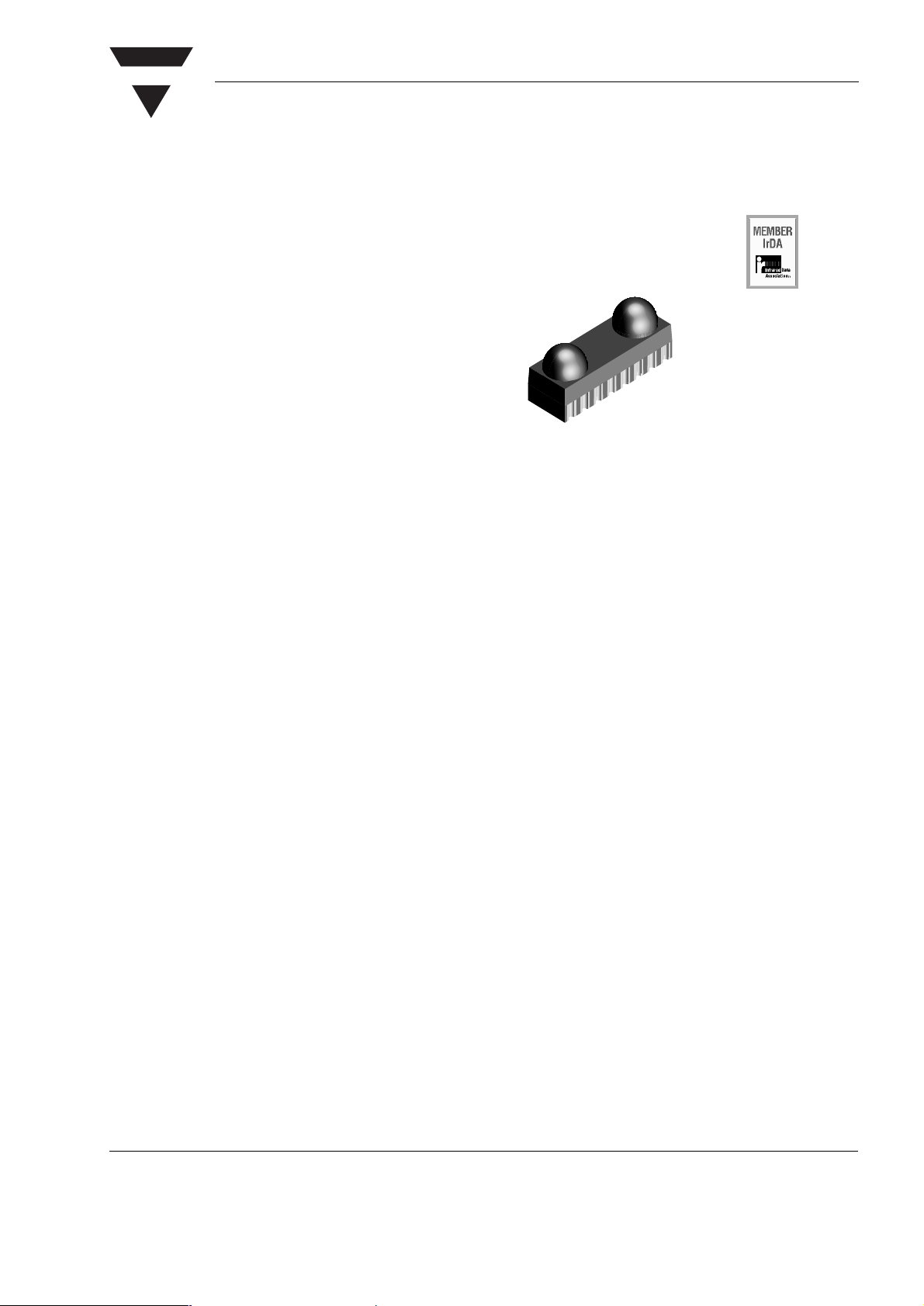
TFBS6614
Vishay Semiconductors
Lowest Profile 4 Mbits/s (FIR) Infrared Transceiver Module
Description
The Vishay TFBS6614 is the lowest profile (2.7 mm)
4 Mbit/s Infrared Data Transceiver module available.
A PIN photodiode, an infrared emitter (IRED) and a
low-power CMOS control IC are integrated in a single
package that provides a total front-end solution.
V
directly to TxD, RxD and SD/Mode logic signals of the
transceiver hence eliminating the need for costly signal level converter and reducing power consumption.
The TxD-echo function is enabled for internal selftest. During transmission the TxD signals are echoed
at RxD output to perform the internal self-test.
- allows a low-voltage controller to connect
LOGIC
The Shut Down (SD) feature cuts current consumption to less than 10 nA.
Features
• Smallest FIR Transceiver available:
H 2.7 mm x W 3.33 mm x L 7.98 mm
• 1.0 m Link distance
• Battery & Power Management Features:
> Receive - 2 mA Typical
> Shutdown - 10 nA Typical
> Independent LED Anode Power Supply
> Wide Voltage Range 2.7 V - 5.5 V
> Power Up Latency < 100 µs
> High V
• The TxD-Echo function is enabled
•V
LOGIC
voltage
• Shutdown Tri-States Receiver Output and Disables TxD allowing Bus Interfacing
• High Immunity to Fluorescent Light Noise and AC
Field. No external shield required
• High DC Ambient Rejection - Operates Outdoors
• Receiver Latency Less than 100 µs
• Directly Interfaces with Various Super I/O and
Controller Devices
Noise Rejection > 100 m VPP
CC
(1.5 V - 5.5 V) - Independent Digital supply
Applications
PDAs
Mobile Phones
Notebook Computers, Desktop PCs
Digital Still and Video Cameras
External Infrared Adapters (Dongles)
Diagnostics Systems
Medical and Industrial Data Collection Devices
GPS
Document Number 82611
Rev. 1.4, 28-Oct-03
www.vishay.com
1
Page 2
TFBS6614
Vishay Semiconductors
Parts Table
Part Description Qty / Reel
TFBS6614-TR3 Oriented in carrier tape for side view surface mounting 2500 pcs
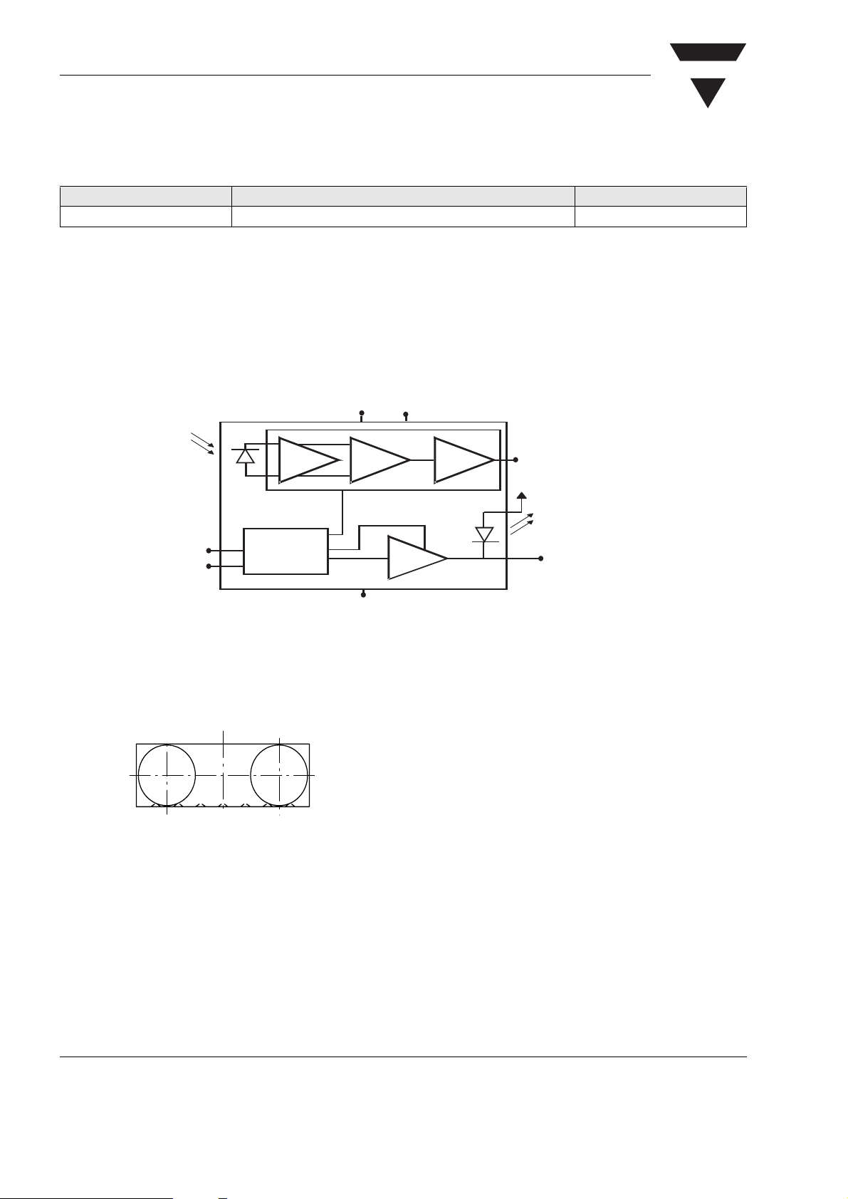
Functional Block Diagram
VISHAY
18072
Pinout
TFBS6614
weight 80 mg
SD/Mode
TxD
Amp
Mode &
Power
Control
V
CC1
Comp
GND
V
Driver
logic
Driver
V
RxD
CC2
LEDA
LEDC
18304
www.vishay.com
2
1234567
Document Number 82611
Rev. 1.4, 28-Oct-03
Page 3
VISHAY
TFBS6614
Vishay Semiconductors
Absolute Maximum Ratings
Reference Point Ground, Pin 8, unless otherwise noted
Parameter Test Conditions Symbol Min Ty p. Max Unit
Analog Supply Voltage Range,
all states
Digital Supply Voltage Range V
Input Current During Transmit, VCC = 5.0 V,
TxD = V
DD
Output Sink Current, RxD 25.0 mA
Peak IRED Current V
Average IRED Current V
Power Dissipation 500 mW
Junction Temperature 125 °C
Ambient Temperature Range
(Operating)
Storage Temperature Range T
Soldering Temperature t = 20 s @ 215 °C 215 240 °C
Transmitter Data and Shutdown
Input Voltage
Receiver Data Output Voltage RxD - 0.5 VDD +
= 2.7 V, TxD = VDD, 125 ns
CC1
pulse
= 2.7 V 125 mA
CC2
V
CC1
DD
T
A
S
V
, V
TxD
SD
- 0.5 + 6.0 V
- 0.5 + 6.0 V
10.0 mA
650 mA
- 25 + 85 °C
- 25 + 85 °C
- 0.5 VDD +
0.5
0.5
V
V
Optoelectronic Characteristics
Receiver
TA = 25 °C, VCC = 2.7 V to 5.5 V unless othervise noted
Parameter Test Conditions Symbol Min Ty p. Max Unit
Minimum Detection Threshold
Irradiance
Analog Supply Voltage Range Specified operation V
Digital Supply Voltage Range Specified operation V
Maximum LED Anode Voltage V
ICC Shut Down Current VCC = 5 V I
ICC Idle Current VCC = 5 V I
4.0 Mbit/s,
l = 850 nm to 900 nm
Transmitter
TA = 25 °C, VCC = 2.7 V to 5.5 V unless othervise noted
Parameter Test Conditions Symbol Min Ty p. Max Unit
Output Radiant Intensity α = 0 °C, 15 °C,
TxD = High, SD = Low
E
e
CC
DD
LEDA
CC1
CC2
I
e
100
2.7 5.5 V
1.5 5.5 V
VCC + 4 V
0.01 2.0 µA
1.6 mA
110 mW/sr
mW/m
2
Document Number 82611
Rev. 1.4, 28-Oct-03
www.vishay.com
3
Page 4

TFBS6614
Vishay Semiconductors
VISHAY
Mode Switching
Upon power-up the TFBS6614 module initializes in
the SIR (9.6 kbit/s to 115.2 kbit/s) mode.The module
can be switched to higher bandwidth and vice versa
by using the sequence described bellow:
SD/Mode 50%
t
s
TxD 50% 50%
18073
Figure 1. Mode Switching Timing Diagram
t
h
High: FIR
Low:
SIR/ MIR
Setting to the High Bandwidth Mode (0.576 Mbit/s to 4 Mbit/s)
1. Set SD/ Mode input to logic "High".
2. Set TxD input to logic "High". Wait ts ≥ 200 ns.
3. Set SD/ Mode to logic "Low" (the negative edge
latches state of TxD, which determines data rate setting).
4. After waiting th ≥ 200 ns TxD can be set to logic
"Low". The hold time of TxD is limited by the maximum allowed pulse width.
TxD is now enabled as normal TxD input for the high
bandwidth mode.
Setting to the Lower Bandwidth Mode (9.6 kbit/s to 115.2 kbit/s)
1. Set SD/ Mode input to logic "High".
2. Set TxD input to logic "Low". Wait ts ≥ 200 ns.
3. Set SD/ Mode to logic "Low" (the negative edge
latches state of TxD, which determines data rate setting).
4. After waiting th ≥ 200 ns TxD can be set to logic
"Low". The hold time of TxD is limited by the maximum allowed pulse width.
TxD is now enabled as normal TxD input for the lower
bandwidth mode.
Recommended Solder Profile
18075
260
240
220
200
180
160
140
120
100
Temperature /°C
80
60
40
20
0
0 50 100 150 200 250 300 350
2...4°C/s
240°C max.
160°C max.
120 s...180 s
Time/s
10 s max. @ 230°C
2-4°C/s
90 s max.
www.vishay.com
4
Document Number 82611
Rev. 1.4, 28-Oct-03
Page 5

VISHAY
Recommended Circuits
TFBS6614
Vishay Semiconductors
18076
VCC=3.3 V
VDD=1.8 V
IR Controller
IRMODE
Circuit Diagram with separate V and V
(I/O voltage follows V voltage swing)
Vdd
DD
R2
3.3Ω
CC
IRTX
IRRX
R1
47Ω
C3
GND
C1
4.7 µF
C2
0.1µF
4.7µF
C4
0.1 µFC50.1 µF
LOGIC
TFBS6614
1 LEDA
2LEDC
3 TxD
4 RxD
5SD
6 Vcc
7 Vlogic
8 GND
18077
Circuit Diagram with a Common Power Supply for V and V
VCC= 3.3 V
IR Controller
IRMODE
(I/O voltage follows V voltage swing)
Vdd
IRTX
IRRX
GND
C1
4.7µFC20.1mΦC34.7µF
CC
R2
3.3Ω
R1
47Ω
C4
0.1µF
CC
TFBS6614
1LEDA
2LEDC
3 TxD
4 RxD
5SD
6 Vcc
7 Vlogic
8 GND
LOGIC
Document Number 82611
Rev. 1.4, 28-Oct-03
www.vishay.com
5
Page 6

TFBS6614
Vishay Semiconductors
Package Dimensions in mm
VISHAY
www.vishay.com
6
18074
Document Number 82611
Rev. 1.4, 28-Oct-03
Page 7

VISHAY
Reel Dimensions
TFBS6614
Vishay Semiconductors
W
1
Reel Hub
W
2
Tape Width A max. N W1 min. W2 max. W3 min. W3 max.
mm mm mm mm mm mm mm
24 330 60 24.4 30.4 23.9 27.4
14017
Document Number 82611
Rev. 1.4, 28-Oct-03
www.vishay.com
7
Page 8

TFBS6614
Vishay Semiconductors
Tape Dimensions in mm
VISHAY
18297
www.vishay.com
8
Document Number 82611
Rev. 1.4, 28-Oct-03
Page 9

VISHAY
TFBS6614
Vishay Semiconductors
Ozone Depleting Substances Policy Statement
It is the policy of Vishay Semiconductor GmbH to
1. Meet all present and future national and international statutory requirements.
2. Regularly and continuously improve the performance of our products, processes, distribution and
operatingsystems with respect to their impact on the health and safety of our employees and the public, as
well as their impact on the environment.
It is particular concern to control or eliminate releases of those substances into the atmosphere which are
known as ozone depleting substances (ODSs).
The Montreal Protocol (1987) and its London Amendments (1990) intend to severely restrict the use of ODSs
and forbid their use within the next ten years. Various national and international initiatives are pressing for an
earlier ban on these substances.
Vishay Semiconductor GmbH has been able to use its policy of continuous improvements to eliminate the
use of ODSs listed in the following documents.
1. Annex A, B and list of transitional substances of the Montreal Protocol and the London Amendments
respectively
2. Class I and II ozone depleting substances in the Clean Air Act Amendments of 1990 by the Environmental
Protection Agency (EPA) in the USA
3. Council Decision 88/540/EEC and 91/690/EEC Annex A, B and C (transitional substances) respectively.
Vishay Semiconductor GmbH can certify that our semiconductors are not manufactured with ozone depleting
substances and do not contain such substances.
We reserve the right to make changes to improve technical design
and may do so without further notice.
Parameters can vary in different applications. All operating parameters must be validated for each
customer application by the customer. Should the buyer use Vishay Semiconductors products for any
unintended or unauthorized application, the buyer shall indemnify Vishay Semiconductors against all
claims, costs, damages, and expenses, arising out of, directly or indirectly, any claim of personal
damage, injury or death associated with such unintended or unauthorized use.
Vishay Semiconductor GmbH, P.O.B. 3535, D-74025 Heilbronn, Germany
Telephone: 49 (0)7131 67 2831, Fax number: 49 (0)7131 67 2423
Document Number 82611
Rev. 1.4, 28-Oct-03
www.vishay.com
9
 Loading...