

Page 1
❇
TESTING
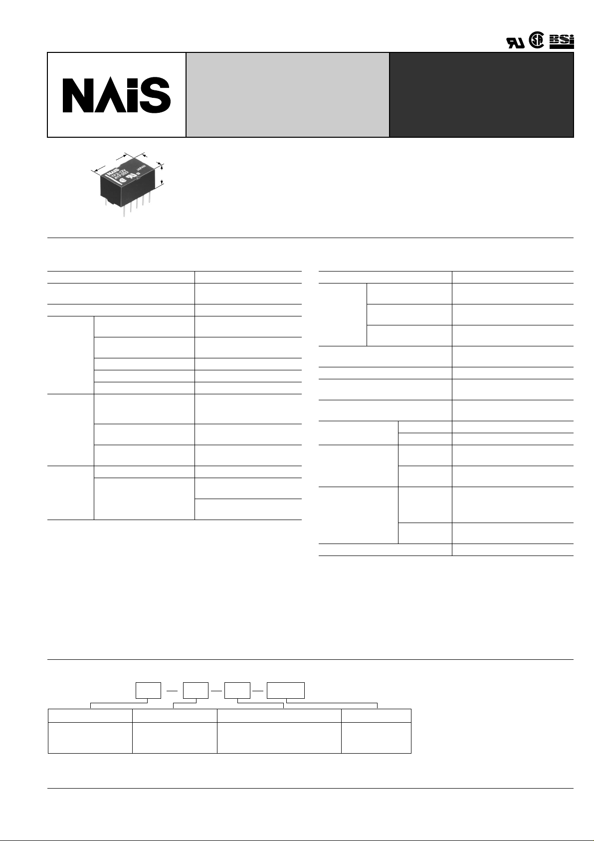
SMALL POLARIZED RELAY
WITH HIGH SENSITIVITY
TF-RELAYS
14
.551
.354
9
7.8
.307
FEATURES
• High sensitivity:
80 mW Nominal operating power (Single
side stable 3-12 V type)
• Surge voltage withstand: 1500 V FCC
Part 68
mm inch
SPECIFICATIONS
Contact
Arrangement 2 Form C
Initial contact resistance, max.
(By voltage drop 6 V DC 1 A)
Contact material Gold-clad silver
Nominal switching
capacity (resistive load)
1 A 30 V DC, 0.5 A 125 V AC
Max. switching power
Rating
(resistive load)
Max. switching voltage 110 V DC, 125 V AC
Max. switching current 1 A
Min. switching capacity ❇ 1 10 µ A 10 mV DC
Single side stable
Nominal
operating
power
1 coil latching
2 coil latching
Mechanical (at 180 cpm) 10
Expected
life (min.
operations)
Electrical (at 20 cpm)
1 A 30 V DC resistive load
0.5 A 125 V AC resistiv e load
Note:
1This value can change due to the switching frequency, en vironmental conditions,
and desired reliability level, therefore it is recommended to chec k this with the actual load.
50 m Ω
30 W, 62.5 VA
80 mW (3 to 12 V DC)
140 mW (24 V DC)
260 mW (48 V DC)
55 mW (3 to 12 V DC)
100 mW (24 V DC)
110 mW (3 to 12 V DC)
200 mW (24 V DC)
8
5
2 × 10
5
10
• Minimal magnetic interference allows
high density mounting
• Sealed construction allows automatic
cleaning
• Self-clinching terminal also available
Characteristics
Initial insulation resistance*
Between open
Initial
breakdown
voltage
contacts
Between contact and
coil
Between contact sets
FCC surge voltage between open
contacts
Temperature rise*
2
(at 20 ° C) Max. 50 ° C
Operate time [Set time]*
Release time [Reset time]*
(at 20 ° C)
Shock resistance
Vibration resistance
Conditions for operation, transport and
8
storage*
(Not freezing and
condensing at low
temperature)
Unit weight Approx. 2 g .071 oz
Remarks
* Specifications will vary with foreign standards certification ratings.
*1
Measurement at same location as "Initial breakdown voltage" section.
*2
By resistive method, nominal voltage applied to the coil; contact carrying current:
1 A.
*3
Nominal voltage applied to the coil, excluding contact bounce time.
*4
Nominal voltage applied to the coil, excluding contact bounce time without diode.
*5
Half-wave pulse of sine wave: 11 ms; detection time: 10 µ s.
*6
Half-wave pulse of sine wave: 6 ms.
*7
Detection time: 10 µ s.
*8
Refer to 4. Conditions f or operation, transport and storage mentioned in Cautions
for use (Page 178).
1
Min. 1,000 M Ω (at 500 V DC)
750 Vrms for 1 min.
(Detection current: 10 mA)
1,000 Vrms for 1 min.
(Detection current: 10 mA)
1,000 Vrms for 1 min.
(Detection current: 10 mA)
1,500 V
3
(at 20 ° C)
4
Max. 4 ms (Approx. 2 ms)
[Max. 4 ms (Approx. 2 ms)]
Max. 4 ms (Approx. 1 ms)
[Max. 4 ms (Approx. 2 ms)]
Functional*
Destructive*
Functional*
Destructive
Ambient
temperature
5
6
7
Min. 490 m/s
Min. 980 m/s
176.4 m/s
at double amplitude of 3 mm
2
294 m/s
at double amplitude of 5 mm
–40 ° C to +70 ° C
–40 ° F to +158 ° F
2
{50 G}
2
{100 G}
2
{18G}, 10 to 55 Hz
{30G}, 10 to 55 Hz
Humidity 5 to 85% R.H.
ORDERING INFORMATION
Ex. TF 2 L H 3V
Contact arrangement Operating function Terminal shape Coil voltage(DC)
2:2 Form C Nil: Standard PC board terminal
*
48 V coil type: Single side stable only
Note: AgPd stationary contact types available for high resistance against contact sticking.
When ordering, please add suffix“-3”like TF2-12V-3.
Nil: Single side stable
L: 1 coil latching
L2: 2 coil latching
H: Self-clinching terminal
3,4.5,5,6,9,12,
24,48
*
V
145
Page 2
Ω ( ±
Ω ( ±
Ω ( ±
TF
TYPES AND COIL DATA (at 20 ° C 68 ° F)
1. Single side stable
Standard PC
board terminal
Part No.
Self-clinching
terminal
Nominal
voltage,
V DC
Pick-up
voltage,
V DC (max.)
Drop-out
voltage,
V DC (min.)
TF2-3 V TF2-H-3 V 3 2.25 0.3 26.7 112.5 80 4.5
TF2-4.5 V TF2-H-4.5 V 4.5 3.38 0.45 17.8 253 80 6.7
TF2-5 V TF2-H-5 V 5 3.75 0.5 16 312.5 80 7.5
TF2-6 V TF2-H-6 V 6 4.5 0.6 13.3 450 80 9
TF2-9 V TF2-H-9 V 9 6.75 0.9 8.9 1,012.5 80 13.5
TF2-12 V TF2-H-12 V 12 9 1.2 6.7 1,800 80 18
TF2-24 V TF2-H-24 V 24 18 2.4 5.8 4,100 140 36
TF2-48 V TF2-H-48 V 48 36 4.8 5.4 8,860 260 57.6
2. 1 Coil latching
Part No.
Standard PC
board terminal
Self-clinching
terminal
TF2-L-3 V TF2-L-H-3 V 3 2.25 2.25 18.3 163.6 55 4.5
TF2-L-4.5 V TF2-L-H-4.5 V 4.5 3.38 3.38 12.2 368.2 55 6.7
TF2-L-5 V TF2-L-H-5 V 5 3.75 3.75 11 454.5 55 7.5
TF2-L-6 V TF2-L-H-6 V 6 4.5 4.5 9.2 654.5 55 9
TF2-L-9 V TF2-L-H-9 V 9 6.75 6.75 6.1 1,472 55 13.5
TF2-L-12 V TF2-L-H-12 V 12 9 9 4.6 2,618 55 18
TF2-L-24 V TF2-L-H-24 V 24 18 18 4.2 5,760 100 36
Nominal
voltage,
V DC
Set voltage,
V DC (max.)
Reset voltage,
V DC (max.)
3. 2 Coil latching
Part No.
Standard PC
board terminal
Self-clinching
terminal
TF2-L2-3 V TF2-L2-H-3 V 3 2.25 2.25 36.7 81.8 110 4.5
TF2-L2-4.5 V TF2-L2-H-4.5 V 4.5 3.38 3.38 24.4 184.1 110 6.7
TF2-L2-5 V TF2-L2-H-5 V 5 3.75 3.75 22 227.3 110 7.5
TF2-L2-6 V TF2-L2-H-6 V 6 4.5 4.5 18.3 327.3 110 9
TF2-L2-9 V TF2-L2-H-9 V 9 6.75 6.75 12.2 736.4 110 13.5
TF2-L2-12 V TF2-L2-H-12 V 12 9 9 9.2 1,309 110 18
TF2-L2-24 V TF2-L2-H-24 V 24 18 18 8.3 2,880 200 36
Notes:
1. Specified value of the pick-up, drop-out, set and reset voltage is with the condition of square wave coil pulse.
2. Standard packing: Tube: 50 pcs.; Case; 1,000 pcs.
3. In case of 5 V drive circuit, it is recommended to use 4.5 V type relay.
4. AgPd stationary contact types available for high resistance against contact sticking. When ordering, please add suffix "-3" like TF2-12V -3.
Nominal
voltage,
V DC
Set voltage,
V DC (max.)
Reset voltage,
V DC (max.)
Nominal
operating
current,
mA ( ± 10%)
Nominal
operating
current,
mA ( ± 10%)
Nominal
operating
current,
mA ( ± 10%)
Coil
resistance,
10%)
Coil
resistance,
10%)
Coil
resistance,
10%)
Nominal
operating
power,
mW
Nominal
operating
power,
mW
Nominal
operating
power,
mW
allowable
voltage,
allowable
voltage,
allowable
voltage,
Max.
V DC
Max.
V DC
Max.
V DC
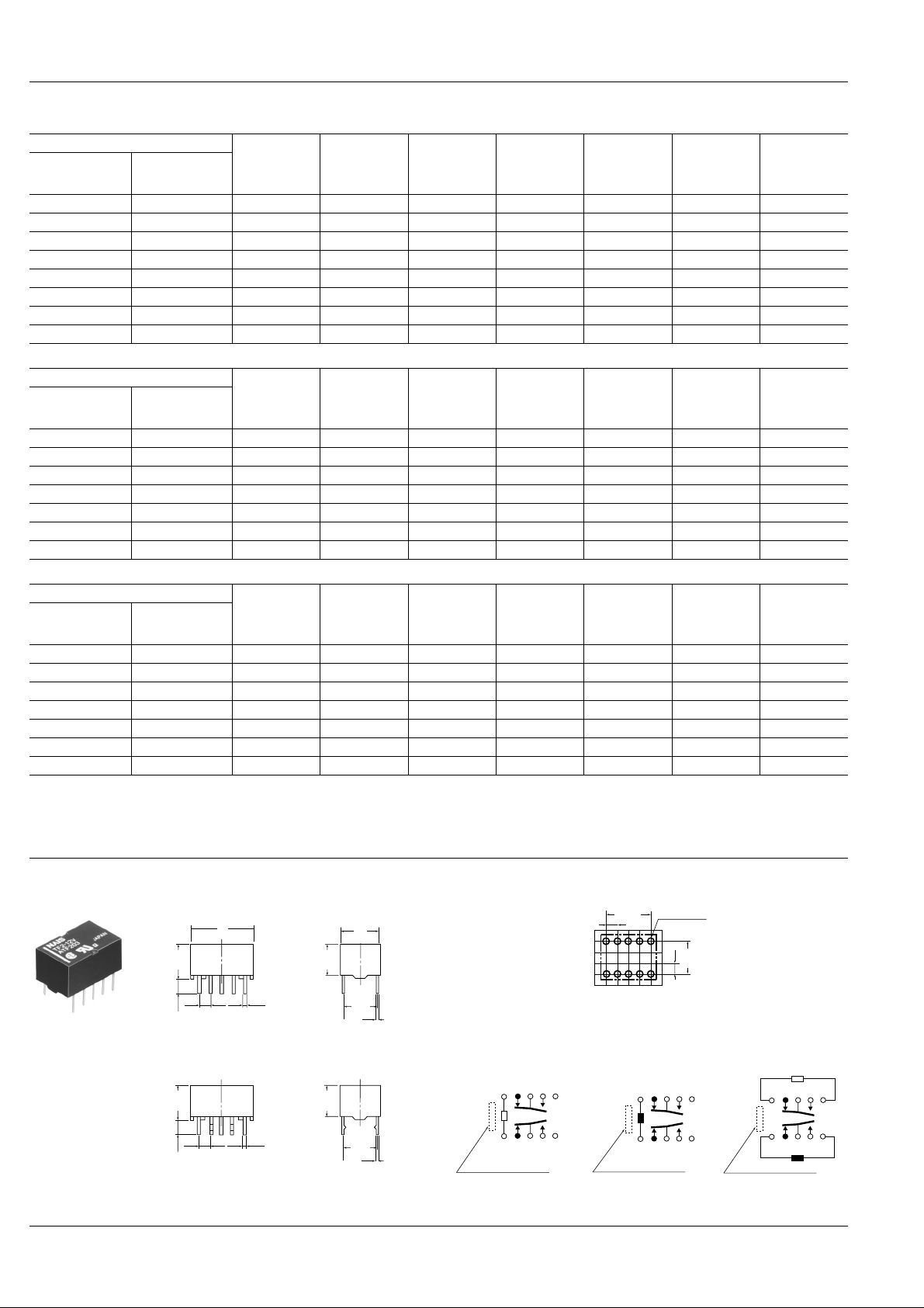
DIMENSIONS
146
Standard PC board terminal
14
.551
7.8
.307
3.5
.138
2.54
0.5
.100
.020
Self-clinching terminal
7.8
.307
3.5
.138
2.54
0.5
.100
.020
General tolerance: ± 0.3 ± .012
.280
7.1
.280
mm inch
PC board pattern
9
.354
7.1
7.62
0.25
.300
.010
(Copper-side view)
Single side stable
(Deenergized condition)
1 2 3 4 5
+
–
7.62
.300
0.25
.010
10 9 8 7 6
Direction indication*
10.16
.400
10-1.0 dia
10-.039 dia
7.62
.300
2.54
.100
2.54
.100
Schematic (Bottom view)
1-coil latching
(Reset condition)
1 2 3 4 5
–
+
10 9 8 7 6
Direction indication*
*Orientation stripe typical-located on top of relay.
Tolerance: ± 0.1 ± .004
2-coil latching
(Reset condition)
1 2 3 4 5
+
+
10 9 8 7 6
Direction indication*
–
–
Page 3

,,
,,,
,,
,,
REFERENCE DATA
1. Maximum switching capacity 2. Life curve 3. Mechanical life
4
100
10
No. of operations, ×10
0 0.5 1.0
30 V DC resistive load
125 V AC resistive load
Switching current, A
1.0
0.5
0.4
Switching current, A
0.3
0.2
DC load (cosϕ=1)
AC load (cosϕ=1)
30 100 200
Switching voltage,V
Tested sample: TF2-12V, 10 pcs.
100
90
80
70
60
50
40
30
20
Ratio against the rated voltage %V
10
0
TF
Pick-up voltage
Drop-out voltage
10 100 1,000 10,000
No. of operations, ×10
Max.
Min.
Max.
Min.
4
4.-(1) Electrical life (DC load)
Tested sample: TF2-12V, 6 pcs.
Condition: 1 A 30 V DC resistive load, 20 cpm
Change of pick-up and drop-out voltage Change of contact resistance
100
90
80
70
60
50
40
30
20
Ratio against the rated voltage, %V
10
Pick-up voltage
Drop-out voltage
0510
No. of operations, ×10
15 20
4
Max.
Min.
Max.
Min.
100
90
80
70
60
50
40
Contact resistance, mΩ
30
20
10
0510
No. of operations, ×10
5. Coil temperature rise
Tested sample: TF2-xxV
Measured portion: Inside the coil
Change of contact resistance
100
90
80
70
60
50
40
Contact resistance, mΩ
30
20
10
05
No. of operations, ×10
Max.
Min.
10
4
Ambient temperature: 30 ° C 86 ° F
Nominal coil voltage
70
60
50
40
30
Temperature rise, °C
20
10
0 100 110 120 130 140 150
3-12 V DC
24 V DC
48 V DC
Coil applied voltage, %V
15 20
4
1 A
1 A
1 A
0 A
Max.
Min.
4.-(2) Electrical life (AC load)
Tested sample: TF2-12V, 6 pcs
Condition: 0.5 A 125 V AC resistive load, 20 cpm
Change of pick-up and drop-out voltage
100
90
80
70
60
50
40
30
20
Ratio against the rated voltage, %V
10
05
Pick-up voltage
Drop-out voltage
No. of operations, ×10
4
6. Operate/release time characteristics
Tested sample: TF2-12V, 5 pcs.
6
5
4
3
2
Operate/release time, ms
1
0 80 90 100 110 120
Operate time
Release time
Coil applied voltage, %V
Max.
Min.
Max.
Min.
Max.
Min.
Max.
Min.
10
7. Set/reset time characteristics
Tested sample: TF2-L2-12V, 5 pcs.
6
5
4
3
Set/reset time, ms
2
1
0 80 90 100 110 120
Coil applied voltage, %V
Set time
Reset time
Max.
Min.
8. Distribution of pick-up and drop-out voltage
Tested sample: TF2-12V, 50 pcs.
30
Drop-out
voltage
20
Quantity
10
010
20 30 40 50 60 70 80 90 100
Ratio against the rated voltage, %V
Pick-up
voltage
9. Distribution of set and reset voltage
Tested sample: TF2-L2-12V, 20 pcs.
Set voltage
Reset voltage
10
Quantity
5
20100
30 40 50 60 70 80 90 100
Ratio against the rated voltage, %V
147
Page 4

TF
10. Ambient temperature characteristics
Tested sample: TF2-12V, 5 pcs.
40
30
Drop-out
voltage
ratio, %
Variation
20
10
Pick-up voltage
0
–20–40
Ambient
temperature, °C
20
40 60 80
–10
–20
–30
–40
11. Distribution of contact resistance
Tested sample: TF2-12V, 30 pcs. (30, × 4 contacts)
−
x
−
x
60
40
Quantity
20
0
30 40 50
Contact resistance,mΩ
12.-(1) High-frequency characteristics
Tested sample: TF2-xxV
Isolation characteristics
100
Isolation, dB
50
10 100 1,000
Frequency,MHz
13.-(1) Malfunctional shock (single side stable)
Tested sample: TF2-12V, 6 pcs
,
Z
Y
,
Y
X
980m/s
980m/s
,
Z
,
X
Z
X
980m/s
2
2
Deenergized
Y
condition
2
Energized condition
196m/s
392m/s
588m/s
784m/s
980m/s
,
Y
Z
2
980m/s
2
2
2
2
2
980m/s
,
X
2
12.-(2) High-frequency characteristics
Tested sample: TF2-xxV
Insertion loss characteristics
1.0
0.8
Insertion loss, dB
0.6
0.4
0.2
100 100 1,000
Frequency,MHz
13.-(2) Malfunctional shock (latching)
Tested sample: TF2-L-12V, 6 pcs.
,
X
Z
,
X
Y
Z
Y
,
Y
X
980m/s
980m/s
,
Z
980m/s
2
2
2
Y
196m/s
392m/s
588m/s
784m/s
980m/s
,
Reset state
Set state
2
2
2
2
2
Z
980m/s
980m/s
,
X
12.-(3) High-frequency characteristics
Tested sample: TF2-xxV
V.S.W.R.
2.0
1.8
1.6
V.S.W.R.
1.4
1.2
1.0
2
2
TF Relay V.S.W.R., 50Ω
10 100 1,000
Frequency,MHz
14.-(1) Influence of adjacent mounting 14.-(2) Influence of adjacent mounting 14.-(3) Influence of adjacent mounting
OFF
OFF
ON
ON
ON
OFF
10
Pick-up voltage
0
–10
Rate of change, %
10
Drop-out voltage
0
–10
Rate of change, %
05
.197
Inter-relay distance , mm inch
ON
ON
ON
ON
OFF
OFF
OFF
OFF
10
Pick-up voltage
0
–10
Rate of change, %
10
Drop-out voltage
0
–10
Rate of change, %
05
.197
Inter-relay distance , mm inch
ONONON
OFF OFF
OFF
10
Pick-up voltage
0
–10
Rate of change, %
10
Drop-out voltage
0
–10
Rate of change, %
05
.197
Inter-relay distance , mm inch
148
Page 5

15. Actual load test
Change of pick-up and drop-out voltage Change of contact resistance
Tested sample: TF2-12V
(35 mA 48 V DC wire spring relay load)
100
90
Circuit
48 V
DC
500Ω
0.1
µF
0.1
µF
500Ω
Wire spring relay Circuit diagram
80
70
60
50
3
2
40
30
20
Ratio against the rated voltage, %V
10
0
Pick-up voltage
Drop-out voltage
10 20 30 40
No. of operations,×10
For Cautions for Use, see Page 178 and 179.
TF
100
90
Max.
Min.
Max.
Min.
50
4
80
70
60
50
40
30
Contact resistance, mΩ
20
10
0
10 20 30 40 50
No. of operations, ×10
Max.
Min.
4
9/1/2000 All Rights Reserved, © Copyright Matsushita Electric Works, Ltd.
149
Go To Online Catalog
 Loading...