

Datasheet TEF3718SSP, TEF3718SP, TEF3718SDP, TEF3718DP Datasheet (SGS Thomson Microelectronics)
Page 1
.HALF AND FULL-STEP MODES
.BIPOLAR DRIV E OF STEPPER MOTOR FOR
MAXIMUM MOTOR PERFORMANCE
.BUILT-IN PROTECTION DIODES
.WIDE RANGE OF CURRENT CONTROL : 5 TO
1500 mA
.WIDE VOLTAGE RANGE : 10 TO 50 V
.DESIGNED FOR UNSTABILIZED MOTOR
SUPPLY VOLTAGE
.CURRENT LEVELS CAN BE SELECTED IN
STEPS OR VARIED CONTINUOUSLY
.THERMAL OVERLOAD PROTECTION
.ALARM OUTPUT (TEF3718SP) OR PRE-
ALARM OUTPUT (TEF3718SSP)
DESCRIPTION
The TEF3718 and TEF371 8S are bipolar m onolithic
integrated circuits intended to control and drive the
current in one widing of a bipola r stepper motor. The
circuits c ons is t s of an LS - TLL - c om pat i ble logic input, a current sensor, a monos table and an output
stage with built-in protection diodes. Two TEF3718
or TEF3718S and a few external components form
a complete contr ol and driv e unit for LS -T TL or microproce ss or c ont r olle d s te pper m ot or systems.
TEF3718
TEF3718S
STEPPER MOTOR DRIVER
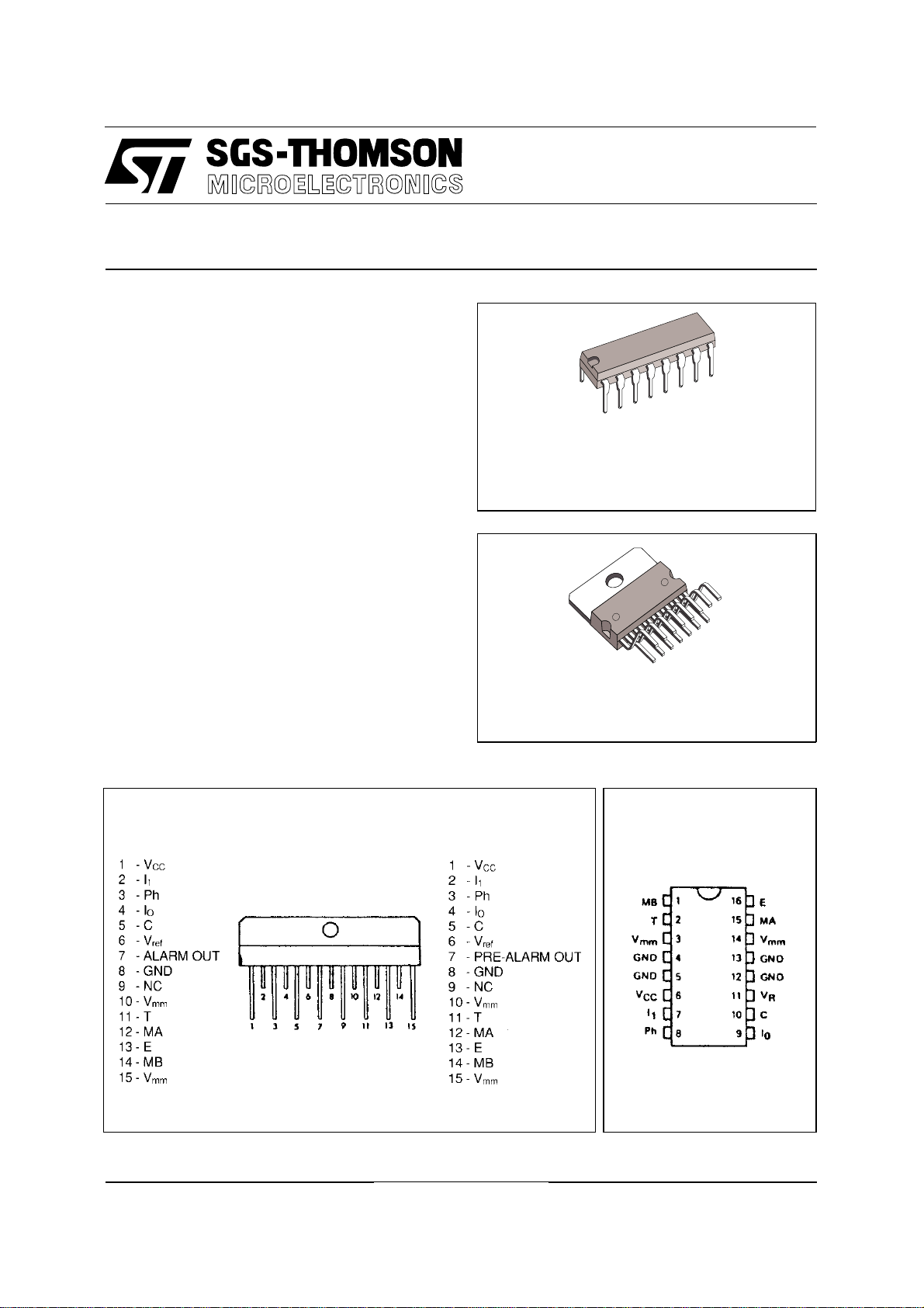
POWERDIP 12 + 2 + 2
ORDER CODE :
TEF3718DP TEF3718SDP
MULTIWATT 15
ORDER CODE :
TEF3718SP TEF3718SSP
PIN CONNECTON
TEF3718 TEF3718 S TEF3718
October 199 1
TEF3718 S
1/8
Page 2
TEF3718-TEF3718S
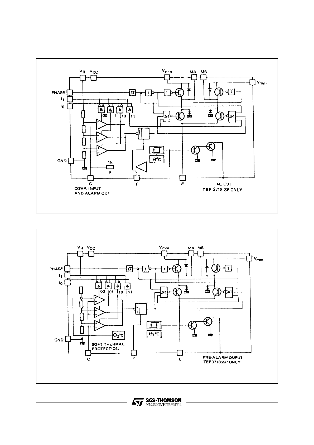
BLOCK DIAGRAM (TEF3718)
BLOCK DIAGRAM (TEF3718S)
2/8
Page 3

TEF3718-TEF3718S
ABSOLUTE MAXIMUM RATINGS
Symbol Parameter Value Unit
V
V
T
T
THERMAL CHARACTERISTICS
Symbol Parameter Value Unit
R
R
Supply Voltage 7
CC
MM
V
Input Voltage :
I
Logic Inputs
Analog Inputs
Reference Input
I
Input Current :
I
Logic Inputs
Analog Inputs
I
Output Current ± 1.5 A
O
T
Junction Temperature + 150 C
j
Operating Ambient Temperature Range – 40 to + 85 °C
oper
Storage Temperature Range – 55 to 150 °C
stg
Maximum Junction-case Thermal Resistance
th(j -c)
POWERDIP
MULTIW
Maximum Junction-ambient Thermal Resistance
th(j -a)
POWERDIP
MULTIW
50
6
V
CC
15
10
10
11
3
45 (*)
40
V
V
mA
°C/W
°C/W
(*) Soldered on a 35 µm thick 20 cm2 PC board coope r area.
RECOMMENDED OPERATING CONDITIONS
Symbol Parameter Min. Typ. Max. Unit
V
V
T
Supply Voltage 4.75
CC
MM
I
Output Current 0.020 – 1.2 A
m
Ambient Temperature – 40 – 85 °C
amb
t
Rise Time Logic Inputs – – 2 µs
r
Fall Time Logic Inputs – – 2 µs
t
f
10
5
–
5.25
45
V
3/8
Page 4

TEF3718-TEF3718S
ELECTRICAL CHARACTERISTICS
= 5 V ± 5 %. VMM = – 10 V to + 45 V. T
V
CC
Symbol Characteristics Min. Typ. Max. Unit
I
V
V
V
V
V
P
Supply Current 25 mA
CC
High Level Input Voltage Logic Input 2 V
IH
V
Low Level Input Voltage Input 0.7 V
IL
I
High Level Input Current Logic Input (VI = 2.4 v) 20 µA
IH
I
Low Level Input Current Logic Input (VI = 0.4 v) 0.4 µA
IL
Comparator Treshold Voltage (VR = + 5 V) IO = 0 I1 = 0
CH
CM
CL
I
Comparator Input Current — 20 20 µA
CO
I
Output Leakage Current (IO 1, I1 = 1) 100 µA
off
Total Saturation Voltage Drop (Im = 1 A,) POWERDIP
sat
Total Power Dissipation (Im = 1 A, fs = 30 kHz) 3.1 3.6 W
tot
t
Cutt off Time (see figures 1 and 2 Vmm = +10 V, V
off
t
Turn off Delay (see figures 1 and 2, T
d
dVC/dt ≤ 50 mV/µs
V
V
Alarm Output Saturation Voltage IO = 2 m A 0.8 V
sat
I
Reference Input Current, VR = 5 V 0.4 1 mA
ref
Source Diode Transistor Pair
sat
= – 40 C to + 25 °C (Unless otherwise specified)
amb
420
250
80
I
= 1 I1 = 0
O
I
= 0 I1 = 1
O
390
230
65
MULTIWATT
≤ 5 µs) 25 30 35 µs
ton
= + 25 °C
amb
1.6 µs
Im = 0.5 A
I
MULTIWATT
= 1 A
m
440
270
90
2.9
3.3
1.35
1.75
mV
V
mA
Saturation Voltage
V
f
POWERDIP
Diode Forward Voltage
I
Substrate Leakage Current
sub
Sink Diode Transistor Pair
MULTIWATT
V
Saturation Voltage
sat
= 0.5 A
I
m
I
= 1 A
m
= 0.5 A
I
f
I
= 1 A
f
I
= 1 A
f
I
= 0.5 A
m
I
= 1 A
m
= 0.5 A
I
m
I
= 1 A
m
1.25
1.55
1.5
1.7
10
1.35
1.55
1.25
1.35
mA
POWERDIP
V
Diode Forward Voltage
f
= 0.5 A
I
f
I
= 1 A
f
1.5
1.8
4/8
Page 5

Figure 1. Figure 2.
TEF3718-TEF3718S
RS = 1 Ω inductance free
= 470 Ω
R
C
= 820 pF ceramic
C
C
= 56 kΩ
R
t
= 820 pF ceramic
C
t
P = 500 Ω
= 1 K
R
2
5/8
Page 6

TEF3718-TEF3718S
MULTIWATT15 PACKAGE MECHANICAL DATA
DIM.
MIN. TYP. MAX. MIN. TYP. MAX.
A 5 0.197
B 2.65 0.104
C 1.6 0.063
D 1 0.039
E 0.49 0.55 0.019 0.022
F 0.66 0.75 0.026 0.030
G 1.02 1.27 1.52 0.040 0.050 0.060
G1 17.53 17.78 18.03 0.690 0.700 0.710
H1 19.6 0.772
H2 20.2 0.795
L 21.9 22.2 22.5 0.862 0.874 0.886
L1 21.7 22.1 22.5 0.854 0.870 0.886
L2 17.65 18.1 0.695 0.713
L3 17.25 17.5 17.75 0.679 0.689 0.699
L4 10.3 10.7 10.9 0.406 0.421 0.429
L7 2.65 2.9 0.104 0.114
M 4.25 4.55 4.85 0.167 0.179 0.191
M1 4.63 5.08 5.53 0.182 0.200 0.218
S 1.9 2.6 0.075 0.102
S1 1.9 2.6 0.075 0.102
Dia1 3.65 3.85 0.144 0.152
mm inch
6/8
Page 7

POWERDIP 16 PACKAGE MECHANICAL DATA
TEF3718-TEF3718S
DIM.
MIN. TYP. MAX. MIN. TYP. MAX.
a1 0.51 0.020
B 0.85 1.40 0.033 0.055
b 0.50 0.020
b1 0.38 0.50 0.015 0.020
D 20.0 0.787
E 8.80 0.346
e 2.54 0.100
e3 17.78 0.700
F 7.10 0.280
I 5.10 0.201
L 3.30 0.130
Z 1.27 0.050
mm inch
7/8
Page 8

TEF3718-TEF3718S
Information furnished is believed to be accurate and reliable. However, SGS-THOMSON Microelectronics assumes no responsibility for
the consequences of use of such information nor for any infringement of patents or other rights of third p arties which may result from its
use. No license is gran ted by implication or otherwise under an y patent or patent rights of SGS-THOMSON Microelectronics. Specifications mentioned in this publication are subject to change without notice. This publication supersedes and replaces all information previously supplied. SGS-THOMSON Microelectronics products are not authorized for use as critical components in life support devices or
systems without express written approval of SGS-THOMSON Microelectronics.
MULTIWATT® is a Registered Trademark of the SGS-THOMSON Microelectronics
Australia - Brazil - France - Germany - Hong Kong - Italy - Japan - Korea - Malaysia - Malta - Morocco - The Netherlands - Singapore -
© 1994 SGS-THOMSON Microelectronics - All Rights Reserved
SGS-THOMSON Microelectronics GROUP OF COMPANIES
Spain - Sweden - Switzerland - Taiwan - Thaliand - United Kingdom - U.S.A.
8/8
 Loading...