

Page 1

DATA SH EET
Product specification
Supersedes data of 1998 Jun 11
File under Integrated Circuits, IC03
1999 Apr 08
INTEGRATED CIRCUITS
TEA1097
Speech and loudspeaker amplifier
IC with auxiliary inputs/outputs and
analog multiplexer
Page 2

1999 Apr 08 2
Philips Semiconductors Product specification
Speech and loudspeaker amplifier IC with
auxiliary inputs/outputs and analog multiplexer
TEA1097
FEATURES
Line interface
• Low DC line voltage
• Voltage regulator with adjustable DC voltage
• Symmetrical high-impedance inputs (70 kΩ) for
dynamic, magnetic or electric microphones
• Dual Tone Multi-Frequency (DTMF) input with
confidence tone on earphone and/or loudspeaker
• Receive amplifier for dynamic, magnetic or
piezo-electric earpieces (with externally adjustable gain)
• Automatic Gain Control (AGC) for true line loss
compensation.
Supplies
• Provides a strong 3.35 V regulated supply for
microcontroller or dialler
• Provides filtered power supply, optimized according to
line current and compatible with external voltage or
current sources
• Filtered 2 V power supply output for electret microphone
• Compatible with a ringer mode
• Power-Down (
PD) logic input for power-down.
Loudspeaker amplifier
• Single-ended rail-to-rail output
• Externally adjustable gain
• Dynamic limiter to prevent distortion
• Logarithmic volume control via linear potentiometer.
Auxiliary interfaces
• Asymmetrical high-impedance input for electret
microphone.
• General purpose auxiliary output for transmit and
receive
• Auxiliary transmit input with high signal level capability
dedicated to line transmission
• Auxiliary receive input with high signal level capability
• Integrated multiplexer for channels selection.
APPLICATIONS
• Telephone answering machines
• Telephones with digital handsfree
• Line powered telephone sets
• Cordless telephones
• Fax machines.
GENERAL DESCRIPTION
The TEA1097 is an analog bipolar circuit dedicated for
telephone applications. It includes a line interface, handset
microphone and earpiece amplifiers, base microphone
and loudspeaker amplifiers, some specific auxiliary
Inputs/Outputs (I/Os) and an analog multiplexer to enable
the right transmit and/or receive channels. The multiplexer
is controlled by a logic circuitry decoding four logic inputs
provided by a microcontroller. Twelve different application
modes have been defined and can be accessed by
selecting the right logic inputs.
This IC can be supplied by the line and/or by the mains if
available (in a cordless telephone or a telephone
answering machine for example). It provides a 3.35 V
supply for a microcontroller or dialler and a 2 V filtered
voltage supply for electret microphones. The IC is
designed to facilitate the use of the loudspeaker amplifier
during ringing phase.
ORDERING INFORMATION
TYPE
NUMBER
PACKAGE
NAME DESCRIPTION VERSION
TEA1097TV VSO40 plastic very small outline package; 40 leads SOT158-1
TEA1097H QFP44 plastic quad flat package; 44 leads (lead length 1.3 mm);
body 10 × 10 × 1.75 mm
SOT307-2
Page 3
1999 Apr 08 3
Philips Semiconductors Product specification
Speech and loudspeaker amplifier IC with
auxiliary inputs/outputs and analog multiplexer
TEA1097
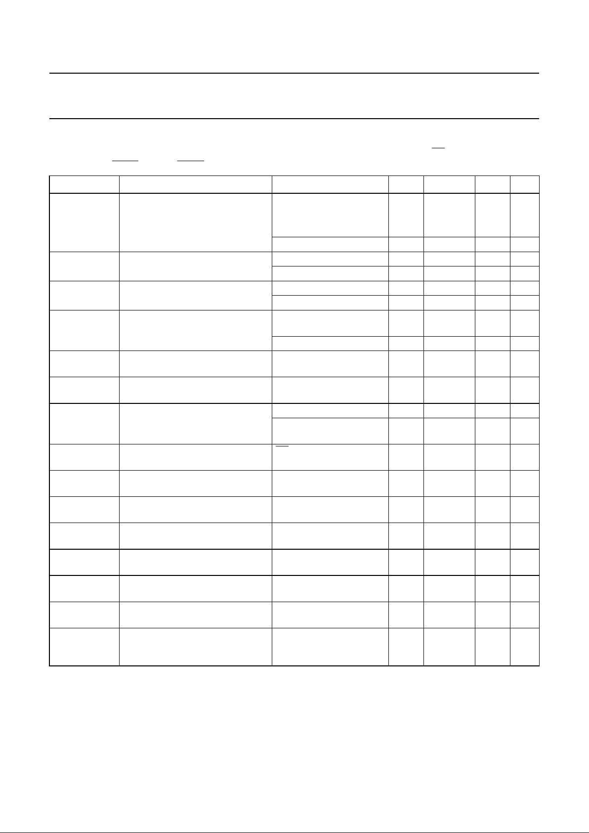
QUICK REFERENCE DATA
I
line
= 15 mA; R
SLPE
=20Ω; Z
line
= 600 Ω; f = 1 kHz; T
amb
=25°C; AGC pin connected to LN;PD = HIGH; HFC = LOW;
AUXC = LOW;
MUTT = HIGH; MUTR = HIGH; measured according to test circuits; unless otherwise specified.
Note
1. When the channel is enabled according to Table 1.
SYMBOL PARAMETER CONDITIONS MIN. TYP. MAX. UNIT
I
line
line current operating range normal operation
TEA1097H 11 − 140 mA
TEA1097TV 11 − 130 mA
with reduced performance 1 − 11 mA
V
SLPE
stabilized voltage between SLPE
and GND (V
ref
)
I
line
= 15 mA 3.4 3.7 4.0 V
I
line
= 70 mA 5.7 6.1 6.5 V
V
BB
regulated supply voltage for
internal circuitry
I
line
= 15 mA 2.75 3.0 3.25 V
I
line
= 70 mA 4.9 5.3 5.7 V
V
DD
regulated supply voltage on
pin V
DD
VBB> 3.35 V + 0.25 V
(typ.)
3.1 3.35 3.6 V
otherwise − V
BB
− 0.25 − V
V
ESI(ext)
external voltage supply allowed on
pin ESI
−− 6V
I
ESI(ext)
external current supply allowed on
pin ESI
−− 140 mA
I
BB
current available on pin V
BB
speech mode − 11 − mA
handsfree mode;
HFC = HIGH
− 9.5 − mA
I
BB(pd)
current consumption on VBB during
power-down phase
PD = LOW − 460 −µA
G
v(MIC-LN)
voltage gain from pin
MIC+/MIC− to LN
V
MIC
= 5 mV (RMS) 43.3 44.3 45.3 dB
G
v(IR-RECO)
voltage gain from pin IR
(referenced to LN) to RECO
VIR= 15 mV (RMS) 28.7 29.7 30.7 dB
∆G
v(QR)
gain voltage range between pins
RECO and QR
−3 − +15 dB
G
v(TXIN-TXOUT)
voltage gain from pin TXIN to
TXOUT
V
TXIN
= 3 mV (RMS);
R
GATX
= 30.1 kΩ; note 1
13.15 14.85 16.55 dB
G
v(TXAUX-LN)
voltage gain from pin TXAUX to LN V
TXAUX
= 0.1 V (RMS);
note 1
11.5 12.5 13.5 dB
G
v(HFRX-LSAO)
voltage gain from pin HFRX to
LSAO
V
HFRX
= 20 mV (RMS);
R
GALS
= 255 kΩ; note 1
25.5 28 30.5 dB
∆G
v(trx)
gain control range for transmit and
receive amplifiers affected by the
AGC; with respect to I
line
=15mA
I
line
= 70 mA; on
G
v(MIC-LN)
, G
v(IR-RECO)
and G
v(IR-AUXO)
5.45 6.45 7.45 dB
Page 4
1999 Apr 08 4
Philips Semiconductors Product specification
Speech and loudspeaker amplifier IC with
auxiliary inputs/outputs and analog multiplexer
TEA1097
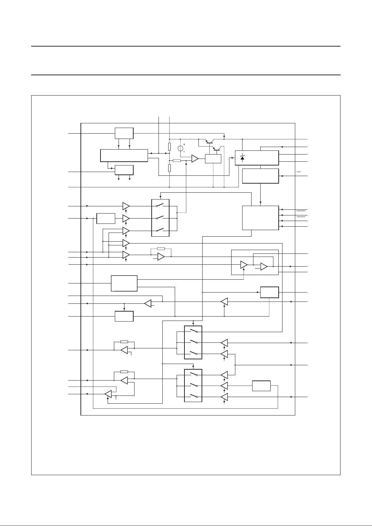
BLOCK DIAGRAM
Fig.1 Block diagram.
The pin numbers given in parenthesis refer to the TEA1097H.
handbook, full pagewidth
MGL392
LINE CURRENT DETECTION
LOW VOLTAGE BEHAVIOUR
TAIL
CURRENTS
SUPPLY
MANAGEMENT
SWITCH
STARTER
AGC
ATT.
ATT.
GND
V
BB
ESI
V
DD
(19) 23
MICS
PD
(10) 13
(9) 12
(20) 24
(38) 40
AGC
LN
17 (13)
22 (18)
19 (15)
REG SLPE
20
(16)18(14)
Tail currents for preamps
STAB 25 (21)
LSAO
16 (12)
DLC 11 (8)
GALS 14 (11)
TXAUX
5 (43)
MIC+
33 (31)
MIC−
32 (30)
DTMF
34 (32)
POWER-DOWN
CURRENT SOURCES
ANALOG
MULTIPLEXER
CONTROL
DYNAMIC
LIMITER
VOLUME
CONTROL
HFC(37) 39
MUTT(39) 1
MUTR(40) 2
AUXC(41) 3
GATX(27) 29
TXOUT
(26) 28
VOL(23) 27
HFRX
(1) 7
HFTX
(36) 38
IR
(17) 21
RAUX
(42) 4
GNDTX(29) 31
TXIN
30 (28)
AUXO
6 (44)
RECO
37 (35)
QR
35 (33)
GARX
36 (34)
TEA1097TV
D6
Page 5
1999 Apr 08 5
Philips Semiconductors Product specification
Speech and loudspeaker amplifier IC with
auxiliary inputs/outputs and analog multiplexer
TEA1097
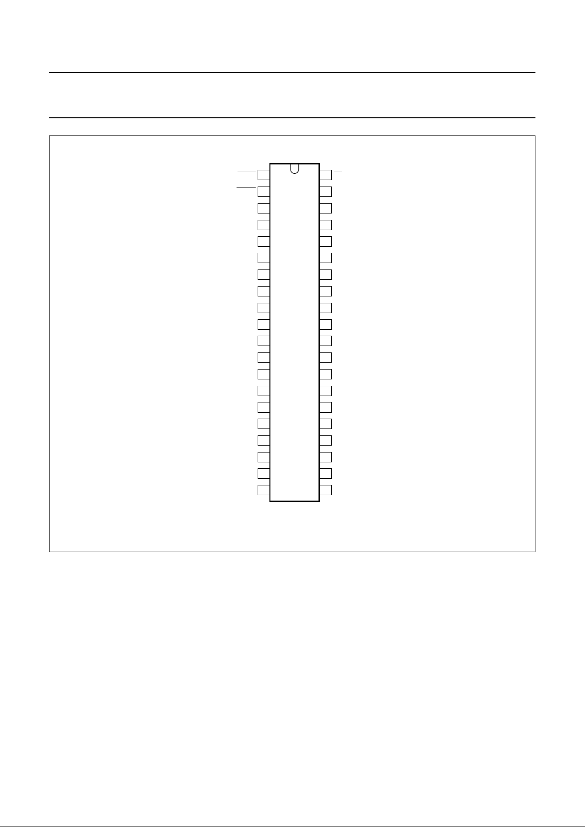
PINNING
SYMBOL
PIN
DESCRIPTION
VSO40 QFP44
MUTT 1 39 logic input (active LOW)
MUTR 2 40 logic input (active LOW)
AUXC 3 41 logic input
RAUX 4 42 auxiliary receive amplifier input
TXAUX 5 43 auxiliary transmit amplifier input
AUXO 6 44 auxiliary amplifier output
HFRX 7 1 receive input for loudspeaker amplifier
n.c. 8 to 10,
15 and 26
2 to 7, 22,
24 and 25
not connected
DLC 11 8 dynamic limiter capacitor for the loudspeaker amplifier
ESI 12 9 external supply input
V
BB
13 10 stabilized supply for internal circuitry
GALS 14 11 loudspeaker amplifier gain adjustment
LSAO 16 12 loudspeaker amplifier output
GND 17 13 ground reference
SLPE 18 14 line current sense
LN 19 15 positive line terminal
REG 20 16 line voltage regulator decoupling
IR 21 17 receive amplifier input
AGC 22 18 automatic gain control/line loss compensation
V
DD
23 19 3.35 V regulated voltage supply for microcontroller
MICS 24 20 microphone supply output
STAB 25 21 reference current adjustment
VOL 27 23 loudspeaker volume adjustment
TXOUT 28 26 base microphone amplifier output
GATX 29 27 base microphone amplifier gain adjustment
TXIN 30 28 base microphone amplifier input
GNDTX 31 29 ground reference for microphone amplifiers
MIC− 32 30 negative handset microphone amplifier input
MIC+ 33 31 positive handset microphone amplifier input
DTMF 34 32 dual tone multi-frequency input
QR 35 33 earpiece amplifier output
GARX 36 34 earpiece amplifier gain adjustment
RECO 37 35 receive amplifier output
HFTX 38 36 transmit input for auxiliary receive amplifier
HFC 39 37 logic input
PD 40 38 power-down input (active LOW)
Page 6
1999 Apr 08 6
Philips Semiconductors Product specification
Speech and loudspeaker amplifier IC with
auxiliary inputs/outputs and analog multiplexer
TEA1097
Fig.2 Pin configuration (VSO40).
handbook, halfpage
TEA1097TV
MGL393
1
2
3
4
5
6
7
8
9
10
11
12
13
14
15
16
17
18
19
20
MUTT
MUTR
AUXC
RAUX
TXAUX
AUXO
HFRX
n.c.
n.c.
n.c.
DLC
ESI
V
BB
GALS
n.c.
LSAO
GND
SLPE
LN
REG
PD
HFC
HFTX
RECO
GARX
QR
DTMF
MIC+
MIC−
GNDTX
TXIN
GATX
TXOUT
VOL
n.c.
STAB
MICS
V
DD
AGC
IR
40
39
38
37
36
35
34
33
32
31
30
29
28
27
26
25
24
23
22
21
Page 7
1999 Apr 08 7
Philips Semiconductors Product specification
Speech and loudspeaker amplifier IC with
auxiliary inputs/outputs and analog multiplexer
TEA1097
Fig.3 Pin configuration (QFP44).
handbook, full pagewidth
1
2
3
4
5
6
7
8
9
10
11
33
32
31
30
29
28
27
26
25
24
23
12
13
14
15
16
17
18
19
20
21
22
44
43
42
41
40
39
38
37
36
35
34
TEA1097H
FCA019
QR
DTMF
MIC+
MIC−
TXIN
GATX
TXOUT
n.c.
n.c.
VOL
HFRX
n.c.
n.c.
n.c
n.c
n.c
DLC
ESI
GALS
GNDTX
TXAUX
RAUX
AUXC
MUTR
MUTT
PD
HFTX
RECO
GARX
AUXO
HFC
GND
SLPE
LN
REG
IR
AGC
MICS
STAB
n.c
LSAO
V
DD
n.c
V
BB
FUNCTIONAL DESCRIPTION
All data given in this chapter are typical values, except
when otherwise specified.
Supplies
L
INE INTERFACE AND INTERNAL SUPPLY (PINS LN, SLPE,
REG
AND V
BB
)
The supply for the TEA1097 and its peripherals is obtained
from the line. The IC generates a stabilized reference
voltage (V
ref
) between pins SLPE and GND. This
reference voltage is equal to 3.7 V for line currents lower
than 18 mA. It than increases linearly with the line current
and reaches the value of 6.1 V for line currents higher than
45 mA. For line currents below 9 mA, the internal
reference voltage generating V
ref
is automatically adjusted
to a lower value. This is the so-called low voltage area and
the TEA1097 has limited performances in this area
(see Section “Low voltage behaviour”). This reference
voltage is temperature compensated.
The voltage between pins SLPE and REG is used by the
internal regulator to generate the stabilized reference
voltage and is decoupled by means of a capacitor between
pins LN and REG.
This capacitor converted into an equivalent inductance
realizes the set impedance conversion from its DC value
(R
SLPE
) to its AC value (done by an external impedance).
The IC regulates the line voltage at pin LN and it can be
calculated as follows:
where:
I
line
= line current
Ix= current consumed on pin LN (approximately a
few µA)
I
SLPE
= current flowing through the R
SLPE
resistor.
V
LN
V
refRSLPE
I×+
SLPE
=
I
SLPEIline
Ix–=
Page 8
1999 Apr 08 8
Philips Semiconductors Product specification
Speech and loudspeaker amplifier IC with
auxiliary inputs/outputs and analog multiplexer
TEA1097
The preferred value for R
SLPE
is 20 Ω. Changing this value
will affect more than the DC characteristics; it also
influences the transmit gains to the line, the gain control
characteristic, the sidetone level and the maximum output
swing on the line.
As can be seen from Fig.4, the internal circuitry is supplied
by pin VBB, which is a strong supply point combined with
the line interface. The line current is flowing through the
R
SLPE
resistor and is sunk by the VBB voltage stabilizer,
becoming available for a loudspeaker amplifier or any
peripheral IC. Its voltage is equal to 3.0 V for line currents
lower than 18 mA. It than increases linearly with the line
current and reaches the value of 5.3 V for line currents
greater than 45 mA. It is temperature compensated.
The aim of the current switch TR1 and TR2 is to reduce
distortion of large AC line signals. Current I
SLPE
is supplied
to VBB via TR1 when the voltage on SLPE is greater than
VBB+ 0.25 V. When the voltage on SLPE is lower than this
value, the current I
SLPE
is shunted to GND via TR2.
The reference voltage V
ref
can be increased by connecting
an external resistor between pins REG and SLPE.
For large line currents, this increase can slightly affect
some dynamic performances such as maximum signal
level on the line for 2% THD. The voltage on pin VBB is not
affected by this external resistor. See Fig.5 for the main
DC voltages.
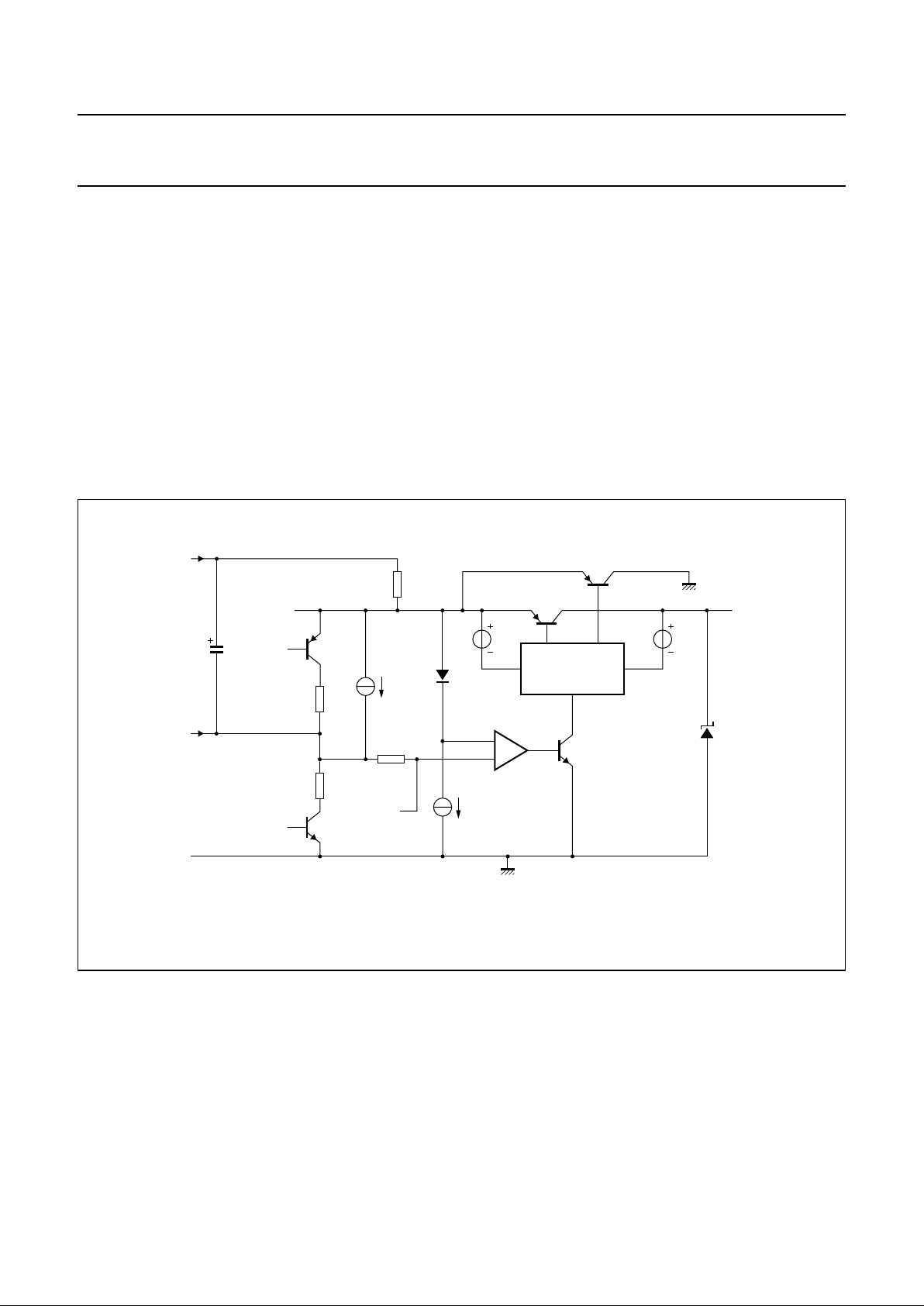
Fig.4 Line interface principle.
handbook, full pagewidth
MGM298
TN2
TR2
TR1
E2
D1
D1
R3
R2
R1
TN1
TP1
J2
J1
E1
GND
GND
V
BB
from
preamp
GND
REG
LN
SLPE
C
REG
4.7 µF
R
SLPE
20 Ω
Page 9
1999 Apr 08 9
Philips Semiconductors Product specification
Speech and loudspeaker amplifier IC with
auxiliary inputs/outputs and analog multiplexer
TEA1097
Fig.5 Main DC voltages as a function of line current.
handbook, full pagewidth
0.070.06
8
6
2
0
0 0.01
voltages
(V)
0.02 0.05
MICS
V
DD
V
BB
SLPE
LN
I
line
(A)
0.040.03
4
FCA049
EXTERNAL SUPPLY (PINS ESI AND VBB)
The TEA1097 can be supplied by the line as well as by
external power sources (voltage or current sources) that
must be connected to pin ESI.
The IC will choose which supply to use according to the
voltage it can provide. A voltage supply on ESI is efficient
only if its value is greater than the working voltage of the
internal V
BB
voltage stabilizer. Otherwise the IC continues
to be line powered. The current consumed on this source
is at least equal to the internal consumption. It depends on
the voltage difference between the value forced on ESI
and the working voltage of the internal stabilizer.
The current required increases with the voltage difference
to manage. The excess current compared to the internal
consumption becomes then available for other purposes
such as supplying a loudspeaker amplifier. The voltage
source should not exceed 6 V. If the value of the external
voltage source can be lower than the working voltage of
the internal stabilizer, an external diode is required to avoid
reverse current flowing into the external power supply.
In case of current source, the voltage on VBB and ESI
depends on the current available. It is internally limited to
6.6 V. The current source should not exceed 140 mA.
V
DD
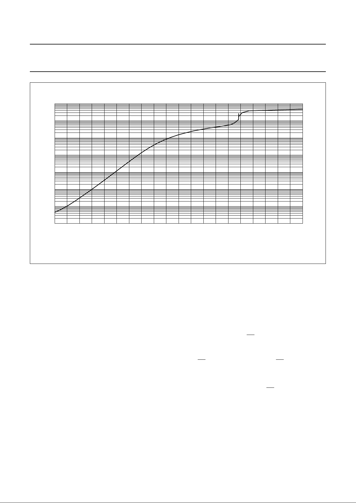
SUPPLY FOR MICROCONTROLLERS (PIN V
DD
)
The voltage on V
DD
supply point follows the voltage on V
BB
with a difference equal to 250 mV (typ.) and is internally
limited to 3.35 V. This voltage is temperature
compensated. This supply point can provide a current up
to 3 mA (typ.). Its internal consumption stays low (a few
10 nA) as long as VDD does not exceed 1.5 V (see Fig.6).
An external voltage can be connected on VDD with limited
extra consumption on VDD (typically 100 µA). This voltage
source should not be lower than 3.5 V and higher than 6 V.
VBB and VDD can supply external circuits in the limits of
currents provided either from the line or from pin ESI,
taking into account the internal current consumption.
Page 10
1999 Apr 08 10
Philips Semiconductors Product specification
Speech and loudspeaker amplifier IC with
auxiliary inputs/outputs and analog multiplexer
TEA1097
Fig.6 Current consumption on VDD.
handbook, full pagewidth
1.0
I
DD
(pA)
1.5 2.5 3.0
VDD (V)
2.0
10
8
10
7
10
6
10
5
10
4
10
3
10
2
10
FCA050
SUPPLY FOR MICROPHONE (PINS MICS AND GNDTX)
The MICS output can be used as a supply for an electret
microphone. Its voltage is equal to 2 V; it can source
current up to 1 mA and has an output impedance equal to
200 Ω.
L
OW VOLTAGE BEHAVIOUR
For line currents below 9 mA, the reference voltage is
automatically adjusted to a lower value; the VBB voltage
follows the SLPE voltage with 250 mV difference.
The excess current available for other purposes than DC
biasing of the IC becomes small. In this low voltage area,
the IC has limited performances.
When the VBB voltage reaches 2.7 V, the VBB detector of
the receive dynamic limiter on pin LSAO acts continuously,
discharging the capacitor at pin DLC. In the DC condition,
the loudspeaker is automatically disabled below this
voltage.
When V
BB
becomes lower than 2.5 V, the TEA1097 is
forced in a low voltage mode whatever the levels on the
logic inputs are. It is a speech mode with reduced
performances only enabling the microphone channel
(between the MIC inputs and LN) and the earpiece
amplifier. These two channels are able to deliver signals
for line currents as small as 3 mA. The HFC input is tied to
GND sinking a current equal to 300 µA (typ.).
P
OWER-DOWN MODE (PINS PD AND AUXC)
To reduce current consumption during dialling or register
recall (flash), the TEA1097 is provided with a power-down
input (
PD). When the voltage on pins PD and AUXC is
LOW, the current consumption from VBB and VDD is
reduced to 460 µA (typ.). Therefore a capacitor of 470 µF
connected to pin VBB is sufficient to power the TEA1097
during pulse dialling or flash. The PD input has a pull-up
structure, while AUXC has a pull-down structure. In this
mode, the capacitor C
REG
is internally disconnected.
Page 11

1999 Apr 08 11
Philips Semiconductors Product specification
Speech and loudspeaker amplifier IC with
auxiliary inputs/outputs and analog multiplexer
TEA1097
RINGER MODE (PINS ESI, VBB, AUXC AND PD)
The TEA1097 is designed to be activated during the
ringing phase. The loudspeaker amplifier can be used for
the melody signal. The IC must be powered by an external
supply on pin ESI, while applying a HIGH level on the logic
input AUXC and a LOW level on the
PD input. Only the
HFRX input and the LSAO output are activated, in order to
limit the current consumption. Some dynamic limiting is
provided to prevent VBB from being discharged below
2.7 V.
Transmit channels (pins MIC+, MIC−, DTMF, TXAUX
and LN)
H
ANDSET MICROPHONE AMPLIFIER (PINS MIC+, MIC− AND
LN)
The TEA1097 has symmetrical microphone inputs.
The input impedance between MIC+ and MIC− is 70 kΩ
(typ.). The voltage gain between pins MIC+, MIC− and LN
is set to 44.3 dB. Without limitation from the output, the
microphone input stage can accommodate signals up to
18 mV (RMS) at room temperature for 2% of THD.
The microphone inputs are biased at one diode voltage.
Automatic gain control is provided for line loss
compensation.
DTMF
AMPLIFIER (PINS DTMF, LN AND RECO)
The TEA1097 has an asymmetrical DTMF input. The input
impedance between pin DTMF and GND is 20 kΩ (typ.).
The voltage gain between pins DTMF and LN is set to
25.35 dB. Without limitation from the output, the input
stage can accommodate signals up to 180 mV (RMS) at
room temperature for 2% of THD.
When the DTMF amplifier is enabled, dialling tones may
be sent on the line. These tones can be heard in the
earpiece or in the loudspeaker at a low level. This is called
the confidence tone. The voltage attenuation between pins
DTMF and RECO is typically equal to −16.5 dB.
The DC biasing of this input is 0 V.
The automatic gain control has no effect on these
channels.
A
UXILIARY TRANSMIT AMPLIFIER (PINS TXAUX AND LN)
The TEA1097 has an asymmetrical auxiliary input TXAUX.
The input impedance between pins TXAUX and GND is
20 kΩ (typ.). The voltage gain between pins TXAUX and
LN is set to 12.5 dB. Without limitation from the output, the
input stage can accommodate signals up to 1.2 V (RMS)
at room temperature for 2% of THD. The TXAUX input is
biased at two diodes voltage.
Automatic gain control is provided for line loss
compensation.
M
ICROPHONE MONITORING ON TXOUT (PINS MIC+, MIC−
AND TXOUT)
The voltage gain between the microphone inputs MIC+,
MIC− and the output TXOUT is set to 49.8 dB. This
channel gives an image of the signal sent on the line while
speaking in the handset microphone. Using external
circuitry, this signal can be used for several purposes such
as sending dynamic limiting or anti-howling in a listening-in
application. The TXOUT output is biased at two diodes
voltage.
The automatic gain control has no effect on these
channels.
Receive channels (pins IR, RAUX, RECO, GARX and
QR)
RX
AMPLIFIER (PINS IR AND RECO)
The receive amplifier has one input IR which is referred to
the line. The input impedance between pins IR and LN is
20 kΩ (typ.) and the DC biasing between these pins is
equal to one diode voltage. The gain between pins IR
(referenced to LN) and RECO is typically equal to 29.7 dB.
Without limitation from the output, the input stage can
accommodate signals up to 50 mV (RMS) at room
temperature for 2% of THD.
This receive amplifier has a rail-to-rail output RECO, which
is designed for use with high-ohmic (real) loads (larger
than 5 kΩ). This output is biased at two diodes voltage.
Automatic gain control is provided for line loss
compensation.
Page 12

1999 Apr 08 12
Philips Semiconductors Product specification
Speech and loudspeaker amplifier IC with
auxiliary inputs/outputs and analog multiplexer
TEA1097
EARPIECE AMPLIFIER (PINS GARX AND QR)
The earpiece amplifier is an operational amplifier having
its output (QR) and its inverting input (GARX) available.
Its input signal comes, via a decoupling capacitor, from the
receive RECO output. It is used in combination with two
resistors to get the required gain or attenuation compared
to the receive gain. It can be chosen between −3 and
+15 dB.
Two external capacitors C
GAR
(connected between pins
GARX and QR) and C
GARS
(connected between pins
GARX and GND) ensure stability. The C
GAR
capacitor
provides a first-order low-pass filter. The cut-off frequency
corresponds to the time constant C
GAR
× Re2.
The relationship C
GARS
≥ 10 × C
GAR
must be fulfilled.
The earpiece amplifier has a rail-to-rail output QR, biased
at two diodes voltage. It is designed for use with low-ohmic
(real) loads (150 Ω) or capacitive loads (100 nF in series
with 100 Ω).
When the amplifier is turned off, the signal present on the
earpiece is equal to the ratio between the load on QR and
Re1+R
e2
AUXILIARY RECEIVE AMPLIFIER (PINS RAUX AND RECO)
The auxiliary receive amplifier has an asymmetrical input
RAUX; it uses the RECO output. Its input impedance
between pins RAUX and GND is typically equal to 20 kΩ.
The voltage gain between pins RAUX and RECO is equal
to−2.4 dB. Without any limitation from the output, the input
stage can accommodate signals up to 0.95 V (RMS) at
room temperature for 2% of THD.
This auxiliary amplifier has a rail-to-rail output RECO,
which is designed for use with high ohmic (real) loads
(larger than 5 kΩ). This output is biased at two diodes
voltage.
The automatic gain control has no effect on this channel.
Auxiliary amplifiers using AUXO (pins MIC+, MIC−,
HFTX, IR and AUXO)
The TEA1097 has an auxiliary output AUXO, biased at two
diodes voltage. This output stage is a rail-to-rail one,
designed for use with high-ohmic (real) loads (larger than
5kΩ). The AUXO output amplifier is used in three different
channels, two transmit channels and one receive channel.
A
UXILIARY AMPLIFIERS USING THE MICROPHONE INPUTS
(PINS MIC+, MIC− AND AUXO)
The auxiliary transmit amplifier using the microphone
MIC+ and MIC− inputs has a gain of 25.5 dB referenced to
AUXO. Without limitation from the output, the input stage
can accommodate signals up to 16 mV (RMS) at room
temperature for 2% of THD.
The automatic gain control has no effect on this channel.
A
UXILIARY AMPLIFIERS USING HFTX (PINS HFTX AND
AUXO)
The auxiliary transmit amplifier using the HFTX input has
a gain of 15.2 dB referenced to AUXO.
The automatic gain control has no effect on this channel.
RX
AMPLIFIER USING IR (PINS IR AND AUXO)
The auxiliary receive amplifier uses pin IR as input.
The input is referenced to pin LN and the DC biasing
between these two pins is one diode voltage. The voltage
gain between the input IR (referenced to LN) and the
output AUXO is typically equal to 32.8 dB, which
compensates typically the attenuation provided by the
anti-sidetone network.
Automatic gain control is provided for line loss
compensation.
Automatic gain control (pin AGC)
The TEA1097 performs automatic line loss compensation,
which fits well with the true line attenuation. The automatic
gain control varies the gain of some transmit and receive
amplifiers in accordance with the DC line current.
The control range is 6.45 dB for G
v(MIC-LN)
, G
v(IR-RECO)
and
G
v(IR-AUXO)
and 6.8 dB for G
v(TXAUX-LN)
, which corresponds
approximately to a line length of 5.5 km for a 0.5 mm
twisted-pair copper cable.
To enable this gain control, the pin AGC must be shorted
to pin LN. The start current for compensation corresponds
to a line current equal to typically 23 mA and the stop
current to 57 mA. The start current can be increased by
connecting an external resistor between pins AGC and LN.
It can be increased to 40 mA (using a resistor typically
equal to 80 kΩ). The start and stop current will be
maintained in a ratio equal to 2.5. By leaving the AGC pin
open-circuit, the gain control is disabled and no line loss
compensation is performed.
Page 13

1999 Apr 08 13
Philips Semiconductors Product specification
Speech and loudspeaker amplifier IC with
auxiliary inputs/outputs and analog multiplexer
TEA1097
Base microphone channel (pins TXIN, GATX, TXOUT
and GNDTX) see Fig.7
The TEA1097 has an asymmetrical base microphone
input TXIN with an input resistance of 20 kΩ.
The DC biasing of the input is 0 V.
The output TXOUT is biased at two diodes voltage and has
a current capability equal to 20 µA (RMS). The gain of the
microphone amplifier (from pins TXIN to TXOUT) can be
adjusted from 0 to 31 dB to suit specific application
requirements.
The gain is proportional to the value of R
GATX
and equals
14.85 dB with R
GATX
= 30.1 kΩ. Without limitation from the
output, the microphone input stage can accommodate
signals up to 18 mV (RMS) at room temperature for 2% of
THD.
A capacitor can be connected in parallel with R
GATX
to
provide a 1st-order low-pass filter.
Fig.7 Base microphone channel.
The pin numbers given in parenthesis refer to the TEA1097H.
handbook, full pagewidth
MGL395
V I I V
C
MIC
V
BB
R
MIC
TXIN
GNDTX
TXOUT
GATX
29
(27)
30
(28)
28
(26)
31
(29)
R
GATX
C
GATX
Page 14

1999 Apr 08 14
Philips Semiconductors Product specification
Speech and loudspeaker amplifier IC with
auxiliary inputs/outputs and analog multiplexer
TEA1097
Loudspeaker channel
Fig.8 Loudspeaker channel.
The pin numbers given in parenthesis refer to the TEA1097H.
handbook, full pagewidth
MGL394
DYNAMIC
LIMITER
VOLUME
CONTROL
I V
V I
DLC
LSAO
GALS
VOL
HFRX
14
(11)
16
(12)
11
(8)
7
(1)
27
(23)
V
BB
R
GALS
C
GALS
C
LSAO
C
DLC
R
VOL
to
logic
LOUDSPEAKER AMPLIFIER: PINS HFRX, GALS AND LSAO
The TEA1097 has an asymmetrical input for the
loudspeaker amplifier with an input resistance of 20 kΩ
between pins HFRX and GND. It is biased at two diodes
voltage. The input stage can accommodate signals up to
580 mV (RMS) at room temperature for 2% of THD.
The rail-to-rail output stage is designed to power a
loudspeaker down to 8 Ω connected as a single-ended
load (between pins LSAO and GND). When the circuit is
externally supplied, the maximum output power is equal to
280 mW (typ.) for 6 V applied to pin ESI.
The gain of the loudspeaker amplifier can be adjusted from
0 to 35 dB to suit specific application requirements.
The gain from HFRX to LSAO is proportional to the value
of R
GALS
and equals 28 dB with R
GALS
= 255 kΩ.
A capacitor connected in parallel with R
GALS
is
recommended and provides a first-order low-pass filter.
V
OLUME CONTROL (PIN VOL)
The loudspeaker amplifier gain can be adjusted with the
potentiometer R
VOL
. A linear potentiometer can be used to
obtain logarithmic control of the gain at the loudspeaker
amplifier. Each 1.9 kΩ increase of R
VOL
results in a gain
loss of 3 dB.
D
YNAMIC LIMITER (PIN DLC)
The dynamic limiter of the TEA1097 prevents clipping of
the loudspeaker output stage and protects the operation of
the circuit when the supply voltage at VBB falls below 2.7 V.
Hard clipping of the loudspeaker output stage is prevented
by rapidly reducing the gain when the output stage starts
to saturate. The time in which gain reduction is effected
(clipping attack time) is approximately a few milliseconds.
The circuit stays in the reduced gain mode until the peaks
of the loudspeaker signals no longer cause saturation.
The gain of the loudspeaker amplifier then returns to its
normal value within the clipping release time (typically
100 ms). Both attack and release times are proportional to
the value of the capacitor C
DLC
. The total harmonic
distortion of the loudspeaker output stage, in reduced gain
mode, stays below 1% up to 10 dB (min.) of input voltage
overdrive [providing V
HFRX
is below 580 mV (RMS)].
When the supply voltage drops below an internal threshold
voltage of 2.7 V, the gain of the loudspeaker amplifier is
rapidly reduced (approximately 1 ms). When the supply
voltage exceeds 2.7 V, the gain of the loudspeaker
amplifier is increased again. By forcing a level lower than
0.2 V on pin DLC, the loudspeaker amplifier is muted.
Page 15

1999 Apr 08 15
Philips Semiconductors Product specification
Speech and loudspeaker amplifier IC with
auxiliary inputs/outputs and analog multiplexer
TEA1097
Logic inputs
Table 1 Selection of transmit and receive channels for 12 different application modes
LOGIC INPUTS
FEATURES APPLICATION EXAMPLES
PD HFC MUTT MUTR AUXC
0 X X X 1 HFRX to LSAO ringer mode
0 X X X 0 flash, DC dialling
10000DTMF to LN; DTMF to RECO;
QR and MICS are active
DTMF dialling in handset
10010MICtoAUXO; RAUX to RECO;
QR and MICS are active
cordless intercom with
corded handset
10110MICtoLN; IR to RECO;
IR to AUXO; MIC to TXOUT ; QR and
MICS are active
handset conversation
10101TXAUX to LN and IR to AUXO conversation using auxiliary
I/O; cordless: digital
handsfree in mobile
11011RAUX to RECO and HFRX to LSAO listening on the loudspeaker
11001TXAUX to LN; IR to AUXO;
RAUX to RECO; HFRX to LSAO
answering machine: play and
record messages; listen the
recorded message on the
loudspeaker
11000DTMF to LN; DTMF to RECO;
HFRX to LSAO; QR and MICS are
active
DTMF dialling in handsfree
or group listening modes
11101TXAUX to LN; IR to AUXO;
IR to RECO and HFRX to LSAO
answering machine: play and
record messages while
listening in the loudspeaker
11010TXIN to TXOUT; HFTX to AUXO;
RAUX to RECO; HFRX to LSAO
and MICS is active
cordless intercom with base
11110TXIN to TXOUT; TXAUX to LN;
IR to RECO; IR to AUXO;
HFRX to LSAO; MICS is active
digital handsfree
conversation
11100MICtoLN; IR to RECO;
IR to AUXO; HFRX to LSAO;
MIC to TXOUT; QR and MICS are
active
handset conversation with
group-listening
Page 16

1999 Apr 08 16
Philips Semiconductors Product specification
Speech and loudspeaker amplifier IC with
auxiliary inputs/outputs and analog multiplexer
TEA1097
LIMITING VALUES
In accordance with the Absolute Maximum Rating System (IEC 134); DC levels are referenced to GND.
THERMAL CHARACTERISTICS
SYMBOL PARAMETER CONDITIONS MIN. MAX. UNIT
V
LN
positive continuous line voltage −0.4 +12 V
repetitive line voltage during switch-on or line
interruption
−0.4 +13.2 V
V
ESI
positive continuous voltage on pin ESI −0.4 +6 V
I
i(ESI)
input current at pin ESI − 140 mA
V
n(max)
maximum voltage
on pins REG, SLPE, IR and AGC −0.4 V
LN
+ 0.4 V
on all other pins except V
DD
−0.4 VBB+ 0.4 V
I
line
maximum line current for
TEA1097H − 140 mA
TEA1097TV − 130 mA
P
tot
total power dissipation T
amb
=75°C
TEA1097TV − 400 mW
TEA1097H − 720 mW
T
stg
IC storage temperature −40 +125 °C
T
amb
operating ambient temperature −25 +75 °C
SYMBOL PARAMETER CONDITIONS VALUE UNIT
R
th(j-a)
thermal resistance from junction to ambient in free air
TEA1097TV 115 K/W
TEA1097H 63 K/W
Page 17

1999 Apr 08 17
Philips Semiconductors Product specification
Speech and loudspeaker amplifier IC with
auxiliary inputs/outputs and analog multiplexer
TEA1097
Fig.9 Safe operating area (TEA1097TV).
LINE T
amb
(°C) P
tot
(mW)
(1) 25 800
(2) 35 720
(3) 45 640
(4) 55 560
(5) 65 480
(6) 75 400
handbook, full pagewidth
160
0
3.5 9.5
(3)
11.5
I
line
(mA)
7.55.5
120
40
80
13.5
V
SLPE
(V)
FCA026
(5)
(6)
(2)
(4)
(1)
Page 18

1999 Apr 08 18
Philips Semiconductors Product specification
Speech and loudspeaker amplifier IC with
auxiliary inputs/outputs and analog multiplexer
TEA1097
Fig.10 Safe operating area (TEA1097H).
LINE T
amb
(°C) P
tot
(mW)
(1) 35 1304
(2) 45 1158
(3) 55 1012
(4) 65 866
(5) 75 720
handbook, full pagewidth
160
0
3 911
I
line
(mA)
75
120
40
80
134 10 1286
V
SLPE
(V)
FCA025
(1)
(2)
(5)
(3)
(4)
Page 19

1999 Apr 08 19
Philips Semiconductors Product specification
Speech and loudspeaker amplifier IC with
auxiliary inputs/outputs and analog multiplexer
TEA1097
CHARACTERISTICS
I
line
= 15 mA; R
SLPE
=20Ω; Z
line
= 600 Ω; f = 1 kHz; T
amb
=25°C; AGC pin connected to LN; PD = HIGH; HFC = LOW;
AUXC = LOW;
MUTT = HIGH; MUTR = HIGH; measured according to test circuits; DC levels are referenced to GND;
unless otherwise specified.
SYMBOL PARAMETER CONDITIONS MIN. TYP. MAX. UNIT
Supplies
L
INE INTERFACE AND INTERNAL SUPPLY (PINS LN, SLPE, REG AND V
BB
)
V
SLPE
stabilized voltage between SLPE
and GND (V
ref
)
I
line
= 15 mA 3.4 3.7 4 V
I
line
= 70 mA 5.7 6.1 6.5 V
V
BB
regulated supply voltage for
internal circuitry
I
line
= 15 mA 2.75 3.0 3.25 V
I
line
= 70 mA 4.9 5.3 5.7 V
I
line
line current for voltage increase start current − 18 − mA
stop current − 45 − mA
∆V
SLPE(T)
stabilized voltage variation with
temperature referenced to 25 °C
T
amb
= −25 to +75 °C −±60 − mV
∆V
BB(T)
regulated voltage variation with
temperature referenced to 25 °C
T
amb
= −25 to +75 °C −±30 − mV
I
BB
current available on pin V
BB
speech mode − 11 − mA
digital handsfree mode;
HFC = HIGH
− 9.5 − mA
V
LN
line voltage I
line
=1mA − 1.55 − V
I
line
=4mA − 2.35 − V
I
line
= 15 mA 3.7 4.0 4.3 V
I
line
= 130 mA − 8.7 9.3 V
EXTERNAL SUPPLY (PIN ESI)
V
ESI
external voltage supply allowed
on pin ESI
−− 6V
voltage on pin ESI when
supplied by a current source
I
ESI
= 140 mA except in
power-down mode
− 6.6 − V
I
i(ESI)
input current on pin ESI V
ESI
= 3.5 V − 3.1 − mA
I
ESI(ext)
external current supply allowed
on pin ESI
−− 140 mA
Page 20

1999 Apr 08 20
Philips Semiconductors Product specification
Speech and loudspeaker amplifier IC with
auxiliary inputs/outputs and analog multiplexer
TEA1097
SUPPLY FOR PERIPHERALS (PIN VDD)
V
DD
regulated supply voltage on V
DDVBB
> 3.35 V + 0.25 V
(typ.)
3.1 3.35 3.6 V
otherwise − V
BB
− 0.25 − V
∆V
DD(T)
regulated voltage variation with
temperature referenced to 25 °C
T
amb
= −25 to +75 °C;
VBB> 3.35 V + 0.25 V
(typ.)
−±30 − mV
I
DD
current consumption on V
DD
in trickle mode;
I
line
= 0 mA;
VDD= 1.5 V;
VBBdischarging
− 15 150 nA
V
DD
> 3.35 V 60 100 −µA
I
DD(o)
current available for peripherals VDD= 3.35 V −− −3mA
SUPPLY FOR MICROPHONE (PIN MICS)
V
MICS
supply voltage for a microphone − 2 − V
I
MICS
current available on MICS −− −1mA
POWER-DOWN INPUT (PIN PD)
V
IL
LOW-level input voltage −0.4 − +0.3 V
V
IH
HIGH-level input voltage 1.8 − VBB+ 0.4 V
I
i(pd)
input current −−3 −6 µA
I
BB(pd)
current consumption on V
BB
during power-down phase
PD = LOW;
AUXC = LOW
− 460 −µA
RINGER MODE (PINS PD, AUXC, HFRX AND LSAO)
I
i(ESI)
input current on pin ESI PD = LOW;
AUXC = HIGH;
V
ESI
= 3.5 V
− 3.1 − mA
G
v(HFRX-LSAO)
voltage gain from pin HFRX to
LSAO
PD = LOW;
AUXC = HIGH;
V
ESI
= 3.5 V
V
HFRX
= 20 mV (RMS);
R
GALS
= 255 kΩ
− 28 − dB
Preamplifier inputs (pins MIC+, MIC−, IR, DTMF, TXIN, HFTX, HFRX, TXAUX and RAUX)
Z
i(MIC)
input impedance
differential between
pins MIC+ and MIC−
− 70 − kΩ
single-ended between
pins MIC+/MIC− and GNDTX
− 35 − kΩ
Z
i(IR)
input impedance between pins
IR and LN
− 20 − kΩ
Z
i(DTMF)
input impedance between pins
DTMF and GND
− 20 − kΩ
Z
i(TXIN)
input impedance between pins
TXIN and GNDTX
− 20 − kΩ
SYMBOL PARAMETER CONDITIONS MIN. TYP. MAX. UNIT
Page 21

1999 Apr 08 21
Philips Semiconductors Product specification
Speech and loudspeaker amplifier IC with
auxiliary inputs/outputs and analog multiplexer
TEA1097
Z
i(HFTX)
input impedance between pins
HFTX and GND
− 20 − kΩ
Z
i(HFRX)
input impedance between pins
HFRX and GND
− 20 − kΩ
Z
i(TXAUX)
input impedance between pins
TXAUX and GND
− 20 − kΩ
Z
i(RAUX)
input impedance between pins
RAUX and GND
− 20 − kΩ
TX amplifiers; see note 1
TX
HANDSET MICROPHONE AMPLIFIER (PINS MIC+, MIC− AND LN)
G
v(MIC-LN)
voltage gain from pin MIC+/MIC−
to LN
V
MIC
= 5 mV (RMS) 43.3 44.3 45.3 dB
∆G
v(f)
gain variation with frequency
referenced to 1 kHz
f = 300 to 3400 Hz −±0.25 − dB
∆G
v(T)
gain variation with temperature
referenced to 25 °C
T
amb
= −25 to +75 °C −±0.25 − dB
CMRR common mode rejection ratio − 80 − dB
THD total harmonic distortion at pinLNVLN = 1.4 V (RMS) −− 2%
I
line
= 4 mA;
VLN= 0.12 V (RMS)
−− 10 %
V
no(LN)
noise output voltage at pin LN;
pins MIC+/MIC− shorted
through 200 Ω
psophometrically
weighted (p53 curve)
−−77.5 − dBmp
∆G
v(mute)
gain reduction if not activated HFC = LOW;
MUTT = LOW;
MUTR = LOW;
AUXC = LOW
60 80 − dB
DTMF AMPLIFIER (PINS DTMF, LN AND RECO)
G
v(DTMF-LN)
voltage gain from pin DTMF toLNV
DTMF
= 50 mV (RMS) 24.35 25.35 26.35 dB
∆G
v(f)
gain variation with frequency
referenced to 1 kHz
f = 300 to 3400 Hz −±0.25 − dB
∆G
v(T)
gain variation with temperature
referenced to 25 °C
T
amb
= −25 to +75 °C −±0.25 − dB
∆G
v(mute)
gain reduction if not activated HFC = LOW;
MUTT = HIGH;
MUTR = HIGH;
AUXC = LOW
60 80 − dB
G
v(DTMF-RECO)
voltage gain from pin DTMF to
RECO
V
DTMF
= 50 mV (RMS) −−16.5 − dB
SYMBOL PARAMETER CONDITIONS MIN. TYP. MAX. UNIT
Page 22

1999 Apr 08 22
Philips Semiconductors Product specification
Speech and loudspeaker amplifier IC with
auxiliary inputs/outputs and analog multiplexer
TEA1097
TX AUXILIARY AMPLIFIER USING TXAUX (PINS TXAUX AND LN)
G
v(TXAUX-LN)
voltage gain from pin TXAUX toLNV
TXAUX
= 0.1 V (RMS) 11.5 12.5 13.5 dB
∆G
v(f)
gain variation with frequency
referenced to 1 kHz
f = 300 to 3400 Hz −±0.25 − dB
∆G
v(T)
gain variation with temperature
referenced to 25 °C
T
amb
= −25 to +75 °C −±0.25 − dB
THD total harmonic distortion at LN V
LN
= 1.4 V (RMS) −− 2%
V
TXAUX(rms)
maximum input voltage at
TXAUX (RMS value)
I
line
= 70 mA; THD = 2% − 1.2 − V
V
no(LN)
noise output voltage at pin LN;
pin TXAUX shorted to GND
through 200 Ω in series with
10 µF
psophometrically
weighted (p53 curve)
−−80.5 − dBmp
∆G
v(mute)
gain reduction if not activated HFC = LOW;
MUTT = LOW;
MUTR = LOW;
AUXC = LOW
60 80 − dB
MICROPHONE MONITORING ON TXOUT (PINS MIC+, MIC− AND TXOUT)
G
v(MIC-TXOUT)
voltage gain from pin MIC+/MIC−
to TXOUT
V
MIC
= 2 mV (RMS) 48.3 49.8 51.3 dB
∆G
v(f)
gain variation with frequency
referenced to 1 kHz
f = 300 to 3400 Hz −±0.1 − dB
∆G
v(T)
gain variation with temperature
referenced to 25 °C
T
amb
= −25 to +75 °C −±0.35 − dB
RX amplifiers; see note 1
RX
AMPLIFIERS USING IR (PINS IR AND RECO)
G
v(IR-RECO)
voltage gain from pin IR
(referenced to LN) to RECO
VIR= 15 mV (RMS) 28.7 29.7 30.7 dB
∆G
v(f)
gain variation with frequency
referenced to 1 kHz
f = 300 to 3400 Hz −±0.25 − dB
∆G
v(T)
gain variation with temperature
referenced to 25 °C
T
amb
= −25 to +75 °C −±0.3 − dB
V
IR(rms)(max)
maximum input voltage on IR
(referenced to LN) (RMS value)
I
line
= 70 mA; THD = 2% − 50 − mV
V
RECO(rms)(max)
maximum output voltage on pin
RECO (RMS value)
THD = 2% 0.75 0.9 − V
V
no(RECO)(rms)
noise output voltage at pin
RECO; pin IR is an open-circuit
(RMS value)
psophometrically
weighted (p53 curve)
−−88 − dBVp
∆G
v(mute)
gain reduction if not activated HFC = LOW;
MUTT = LOW;
MUTR = LOW;
AUXC = LOW
60 80 − dB
SYMBOL PARAMETER CONDITIONS MIN. TYP. MAX. UNIT
Page 23

1999 Apr 08 23
Philips Semiconductors Product specification
Speech and loudspeaker amplifier IC with
auxiliary inputs/outputs and analog multiplexer
TEA1097
RX EARPIECE AMPLIFIER (PINS GARX AND QR)
∆G
v(RECO-QR)
gain voltage range between pins
RECO and QR
−3 − +15 dB
V
QR(rms)(max)
maximum output voltage on pin
QR (RMS value)
sine wave drive;
RL= 150 Ω; THD < 2%
0.75 0.9 − V
V
no(QR)(rms)
noise output voltage at pin QR;
pin IR is an open-circuit
(RMS value)
G
v(QR)
= 0 dB;
psophometrically
weighted (p53 curve)
−−88 − dBVp
RX AMPLIFIER USING RAUX (PINS RAUX AND RECO)
G
v(RAUX-RECO)
voltage gain from pin RAUX to
RECO
V
RAUX
= 0.4 V (RMS) −3.7 −2.4 −1.1 dB
∆G
v(f)
gain variation with frequency
referenced to 1 kHz
f = 300 to 3400 Hz −±0.25 − dB
∆G
v(T)
gain variation with temperature
referenced to 25 °C
T
amb
= −25 to +75 °C −±0.25 − dB
V
RAUX(rms)(max)
maximum input voltage on RAUX
(RMS value)
THD=2% − 0.95 − V
V
no(RECO)(rms)
noise output voltage at pin
RECO; pin RAUX shorted to
GND through 200 Ω in series
with 10 µF (RMS value)
psophometrically
weighted (p53 curve)
−−100 − dBVp
∆G
v(mute)
gain reduction if not activated HFC = LOW;
MUTT = LOW;
MUTR = LOW;
AUXC = LOW
60 80 − dB
Auxiliary amplifiers using AUXO; see note 1
TX
AUXILIARY AMPLIFIER USING MIC+ AND MIC− (PINS MIC+, MIC− AND AUXO)
G
v(MIC-AUXO)
voltage gain from pin MIC+/MIC−
to AUXO
V
MIC
= 10 mV (RMS) 24.2 25.5 26.8 dB
∆G
v(f)
gain variation with frequency
referenced to 1 kHz
f = 300 to 3400 Hz −±0.1 − dB
∆G
v(T)
gain variation with temperature
referenced to 25 °C
T
amb
= −25 to +75 °C −±0.3 − dB
V
MIC(rms)
maximum input voltage on
MIC+/MIC− (RMS value)
THD=2% − 16 − mV
V
no(AUXO)(rms)
noise output voltage at pin
AUXO; pins MIC+/MIC− shorted
to GNDTX through 200 Ω in
series with 10 µF (RMS value)
psophometrically
weighted (p53 curve)
−−91 − dBVp
SYMBOL PARAMETER CONDITIONS MIN. TYP. MAX. UNIT
Page 24

1999 Apr 08 24
Philips Semiconductors Product specification
Speech and loudspeaker amplifier IC with
auxiliary inputs/outputs and analog multiplexer
TEA1097
TX AUXILIARY AMPLIFIER USING HFTX (PINS HFTX AND AUXO)
G
v(HFTX-AUXO)
voltage gain from pin HFTX to
AUXO
V
HFTX
= 100 mV (RMS) 14.2 15.2 16.2 dB
∆G
v(f)
gain variation with frequency
referenced to 1 kHz
f = 300 to 3400 Hz −±0.1 − dB
∆G
v(T)
gain variation with temperature
referenced to 25 °C
T
amb
= −25 to +75 °C −±0.1 − dB
V
AUXO(rms)
maximum output voltage on pin
AUXO (RMS value)
THD = 2% 0.8 0.9 − V
V
no(AUXO)(rms)
noise output voltage at pin
AUXO; pin HFTX shorted to
GND through 200 Ω in series
with 10 µF (RMS value)
psophometrically
weighted (p53 curve)
−−91.5 − dBVp
∆G
v(mute)
gain reduction if not activated HFC = LOW;
MUTT = LOW;
MUTR = HIGH;
AUXC = LOW
60 80 − dB
RX AMPLIFIER USING IR (PINS IR AND AUXO)
G
v(IR-AUXO)
voltage gain from pin IR
(referenced to LN) to AUXO
VIR= 3 mV (RMS) 31.6 32.8 34 dB
∆G
v(f)
gain variation with frequency
referenced to 1 kHz
f = 300 to 3400 Hz −±0.1 − dB
∆G
v(T)
gain variation with temperature
referenced to 25 °C
T
amb
= −25 to +75 °C −±0.3 − dB
V
AUXO(rms)
maximum output voltage on
AUXO (RMS value)
THD = 2% 0.8 0.9 − V
V
no(AUXO)(rms)
noise output voltage at pin
AUXO; pin IR is an open-circuit
(RMS value)
psophometrically
weighted (p53 curve)
−−85 − dBVp
∆G
v(mute)
gain reduction if not activated HFC = HIGH;
MUTT = LOW;
MUTR = HIGH;
AUXC = HIGH
60 80 − dB
Automatic Gain Control (pin AGC)
∆G
v(trx)
gain control range for transmit
and receive amplifiers affected
by the AGC; with respect to
I
line
=15mA
I
line
= 70 mA; on
G
v(MIC-LN)
, G
v(IR-RECO)
and G
v(IR-AUXO)
5.45 6.45 7.45 dB
I
line
= 70 mA;
G
v(TXAUX-LN)
5.8 6.8 7.8 dB
I
start
highest line current for
maximum gain
− 23 − mA
I
stop
lowest line current for maximum
gain
− 57 − mA
SYMBOL PARAMETER CONDITIONS MIN. TYP. MAX. UNIT
Page 25

1999 Apr 08 25
Philips Semiconductors Product specification
Speech and loudspeaker amplifier IC with
auxiliary inputs/outputs and analog multiplexer
TEA1097
Logic inputs (pins HFC, AUXC, MUTT and MUTR)
V
IL
LOW-level input voltage −0.4 − +0.3 V
V
IH
HIGH-level input voltage 1.8 − VBB+ 0.4 V
I
i
input current
for pins HFC and AUXC − 36µA
for pins MUTT and MUTR −−2.5 −6 µA
Base microphone amplifier (pins TXIN, TXOUT and GATX); see note 1
G
v(TXIN-TXOUT)
voltage gain from pin TXIN to
TXOUT
V
TXIN
= 3 mV (RMS);
R
GATX
= 30.1 kΩ
13.15 14.85 16.55 dB
∆G
v
voltage gain adjustment with
R
GATX
−15 − +16 dB
∆G
v(f)
gain variation with frequency
referenced to 1 kHz
f = 300 to 3400 Hz −±0.1 − dB
∆G
v(T)
gain variation with temperature
referenced to 25 °C
T
amb
= −25 to +75 °C −±0.15 − dB
V
no(TXOUT)(rms)
noise output voltage at pin
TXOUT; pin TXIN is shorted
through 200 Ω in series with
10 µF to GNDTX (RMS value)
psophometrically
weighted (p53 curve)
−−101 − dBVp
∆G
v(mute)
gain reduction if not activated HFC = HIGH;
MUTT = LOW;
MUTR = LOW;
AUXC = LOW
60 80 − dB
Loudspeaker amplifier (pins HFRX, LSAO, GALS and VOL); see note 1
G
v(HFRX-LSAO)
voltage gain from pin HFRX to
LSAO
V
HFRX
= 20 mV (RMS);
R
GALS
= 255 kΩ
25.5 28 30.5 dB
∆G
v
voltage gain adjustment with
R
GALS
−28 − +7 dB
∆G
v(f)
gain variation with frequency
referenced to 1 kHz
f = 300 to 3400 Hz −±0.3 − dB
∆G
v(T)
gain variation with temperature
referenced to 25 °C
T
amb
= −25 to +75 °C −±0.3 − dB
∆G
v(vol)
voltage gain variation related to
∆R
VOL
= 1.9 kΩ
−−3 − dB
V
(HFRX)(rms)(max)
maximum input voltage at pin
HFRX (RMS value)
I
line
= 70 mA;
R
GALS
=33kΩ; for 2%
THD in the input stage
− 580 − mV
V
no(LSAO)(rms)
noise output voltage at pin
LSAO; pin HFRX is open-circuit
(RMS value)
psophometrically
weighted (p53 curve)
−−79 − dBVp
V
LSAO(rms)
output voltage (RMS value)
without external supply on pin
ESI
IBB= 0 mA; IDD=1mA
I
line
=18mA − 0.9 − V
I
line
=30mA − 1.2 − V
I
line
>50mA − 1.6 − V
SYMBOL PARAMETER CONDITIONS MIN. TYP. MAX. UNIT
Page 26

1999 Apr 08 26
Philips Semiconductors Product specification
Speech and loudspeaker amplifier IC with
auxiliary inputs/outputs and analog multiplexer
TEA1097
Note
1. When the channel is enabled according to Table 1.
I
LSAO(max)
maximum output current at pin
LSAO (peak value)
external supply on ESI 150 300 − mA
Dynamic limiter (pins LSAO and DLC); see note 1
t
att
attack time when V
HFRX
jumps from
20 mV to 20 mV + 10 dB
−− 5ms
when V
BB
jumps below
V
BB(th)
− 1 − ms
t
rel
release time when V
HFRX
jumps from
20 mV + 10 dB to 20 mV
− 100 − ms
THD total harmonic distortion at
V
HFRX
= 20 mV + 10 dB
t>t
att
− 0.1 2 %
V
BB(th)
VBB limiter threshold − 2.7 − V
Mute Loudspeaker (pin DLC); see note 1
V
DLC(th)
threshold voltage required on pin
DLC to obtain mute receive
condition
−0.4 − +0.2 V
I
DLC(th)
threshold current sourced by pin
DLC in mute receive condition
V
DLC
= 0.2 V − 100 −µA
∆G
vrx(mute)
voltage gain reduction in mute
receive condition
V
DLC
= 0.2 V 60 80 − dB
SYMBOL PARAMETER CONDITIONS MIN. TYP. MAX. UNIT
Page 27

1999 Apr 08 27
Philips Semiconductors Product specification
Speech and loudspeaker amplifier IC with
auxiliary inputs/outputs and analog multiplexer
TEA1097
This text is here in white to force landscape pages to be rotated correctly when browsing through the pdf in the Acrobat reader.This text is here in
_white to force landscape pages to be rotated correctly when browsing through the pdf in the Acrobat reader.This text is here inThis text is here in
white to force landscape pages to be rotated correctly when browsing through the pdf in the Acrobat reader. white to force landscape pages to be ...
TEST AND APPLICATION INFORMATION
o
k, full pagewidth
FCA001
C
IR
100 nF
C
emc
10 nF
i = 15 mA
J_line
C
imp
100 µF
C
REG
4.7 µF
C
VBB
470 µF
C
VDD
47 µF
Z
imp
620 Ω
V
IR
V
HFRX
R
SLPE
20 Ω
R
MIC
200 Ω
C
GATX
100 pF
C
RAUX
100 nF
V
RAUX
C
TXAUX
100 nF
C
DTMF
100 nF
R
GATX
30.1 kΩ
R
STAB
3.65
kΩ
R
VOL
0 to
22 kΩ
R
LSAO
8 Ω
PD
HFC
AUXC
MUTT
MUTR
AUXO
QR
GARX
RECO
HFRX
GALS
LSAO
40
(38)
39
(37)
3
(41)
1
(39)
2
(40)
6
(44)
35
(33)
36
(34)
37
(35)
7
(1)
14
(11)
16
(12)
GND
RAUX
TXAUX
DTMF
GATX
TXOUT
MIC−
MIC+
SLPE REG AGC LN ESI
V
BBVDD
IR
GNDTX STAB VOL DLC
17
(13)31(29)25(21)
27
(23)11(8)
21
(17)
18
(14)20(16)22(18)19(15)12(9)13(10)23(19)
24
(20)
33
(31)
32
(30)
29
(27)
28
(26)
34
(32)
C
HFTX
100 nF
HFTX
MICS
38
(36)
5
(43)
C
TXIN
100 nF
TXIN
30
(28)
4
(42)
TEA1097
from
controller
C
AUXO
10 µF
C
GAR
100 pF
C
GARS
1 nF
C
RXE
100 nF
C
HFRX
100 nF
C
GALS
150 pF
C
GALS
220 µF
C
DLC
470
nF
R
e2
100 kΩ
R
QR
150 Ω
R
e1
100 kΩ
R
AUXO
10 kΩ
R
GALS
255 kΩ
external
supply
D
ESI
Dz
V
d
10 V
C
exch
100 µF
Z
exch
600 Ω
C
MICS
4.7 µF
C
QR
4.7 µF
V
TXAUX
V
MIC
V
DTMF
V
TXIN
V
HFTX
Fig.11 Test circuit.
The pin numbers given in parenthesis refer to the TEA1097H.
Page 28

1999 Apr 08 28
Philips Semiconductors Product specification
Speech and loudspeaker amplifier IC with
auxiliary inputs/outputs and analog multiplexer
TEA1097
This text is here in white to force landscape pages to be rotated correctly when browsing through the pdf in the Acrobat reader.This text is here in
_white to force landscape pages to be rotated correctly when browsing through the pdf in the Acrobat reader.This text is here inThis text is here in
white to force landscape pages to be rotated correctly when browsing through the pdf in the Acrobat reader. white to force landscape pages to be ...
handbook, full pagewidth
MGL396
C
mich
33 nF
C
tx1
C
IR
100 nF
C
bal
220 nF
C
emc
10 nF
C
imp
22 µF
C
REG
4.7 µF
C
VBB
470 µF
C
VDD
47 µF
C
HFTX
100 nF
C
tx2
R
tx1
22 nF
15 kΩ
R
tx2
22 nF
15 kΩ
R
ast1
130 kΩ
R
ast2
3.92 kΩ
R
ast3
392 Ω
R
bal1
130 Ω
Z
imp
620 Ω
R
bal2
820 Ω
R
SLPE
20 Ω
R
tx3
8.2
kΩ
base
microphone
handset
microphone
C
micb
22 nF
C
RAUX
100 nF
C
TXAUX
100 nF
C
DTMF
100 nF
C
TXIN
100 nF
R
STAB
3.65
kΩ
R
bmics
2 kΩ
R
MICM
1 kΩ
R
MICP
1 kΩ
C
MICS
10 µF
R
GATX
30.1 kΩ
R
VOL
0 to
22 kΩ
PD
HFC
AUXC
MUTT
MUTR
AUXO
QR
GARX
RECO
HFRX
GALS
LSAO
40
(38)
39
(37)
3
(41)
1
(39)
2
(40)
6
(44)
35
(33)
36
(34)
37
(35)
7
(1)
14
(11)
16
(12)
GND
RAUX
TXAUX
DTMF
TXIN
GATX
TXOUT
HFTX
MIC−
MIC+
MICS
SLPE REG AGC LN ESI
VBBV
DD
IR
GNDTX STAB VOL DLC
17
(13)31(29)25(21)
27
(23)11(8)
21
(17)
18
(14)20(16)22(18)19(15)12(9)13(10)23(19)
24
(20)
33
(31)
32
(30)
38
(36)
28
(26)
29
(27)
30
(28)
34
(32)
5
(43)
4
(42)
TEA1097
from
controller
C
AUXO
100 nF
C
GAR
100 pF
C
GARS
1 nF
C
RXE
100 nF
C
GALS
150 pF
from digital
handsfree
to digital handsfree
from digital
answering machine
to digital
answering machine
or digital handsfree
from digital
answering machine
or digital handsfree
C
DLC
470
nF
R
e2
100 kΩ
R
e1
100 kΩ
R
GALS
255 kΩ
from MICS
external
supply
D
ESI
Dz
V
d
10 V
D2 D3
D1 D4
A
B
MICS
C
QR
4.7 µF
C
LSAO
220 µF
Fig.12 Basic application diagram.
The pin numbers given in parenthesis refer to the TEA1097H.
Page 29

1999 Apr 08 29
Philips Semiconductors Product specification
Speech and loudspeaker amplifier IC with
auxiliary inputs/outputs and analog multiplexer
TEA1097
PACKAGE OUTLINES
UNIT A
1
A2A
3
b
p
cD
(1)E(2)
Z
(1)
eHELLpQywv θ
REFERENCES
OUTLINE
VERSION
EUROPEAN
PROJECTION
ISSUE DATE
IEC JEDEC EIAJ
mm
inches
0.3
0.1
2.45
2.25
0.25
0.42
0.30
0.22
0.14
15.6
15.2
7.6
7.5
0.762 2.25
12.3
11.8
1.15
1.05
0.6
0.3
7
0
o
o
0.1 0.1
DIMENSIONS (inch dimensions are derived from the original mm dimensions)
Notes
1. Plastic or metal protrusions of 0.4 mm maximum per side are not included.
2. Plastic interlead protrusions of 0.25 mm maximum per side are not included.
1.7
1.5
SOT158-1
92-11-17
95-01-24
X
w M
θ
A
A
1
A
2
b
p
D
H
E
L
p
Q
detail X
E
Z
e
c
L
v M
A
(A )
3
A
y
40
20
21
1
pin 1 index
0.012
0.004
0.096
0.089
0.017
0.012
0.0087
0.0055
0.61
0.60
0.30
0.29
0.03 0.089
0.48
0.46
0.045
0.041
0.024
0.012
0.004
0.2
0.008 0.004
0.067
0.059
0.010
0 5 10 mm
scale
VSO40: plastic very small outline package; 40 leads
SOT158-1
A
max.
2.70
0.11
Page 30

1999 Apr 08 30
Philips Semiconductors Product specification
Speech and loudspeaker amplifier IC with
auxiliary inputs/outputs and analog multiplexer
TEA1097
UNIT A1A2A3b
p
cE
(1)
eH
E
LL
p
Zywv θ
REFERENCES
OUTLINE
VERSION
EUROPEAN
PROJECTION
ISSUE DATE
IEC JEDEC EIAJ
mm
0.25
0.05
1.85
1.65
0.25
0.40
0.20
0.25
0.14
10.1
9.9
0.8 1.3
12.9
12.3
1.2
0.8
10
0
o
o
0.15 0.10.15
DIMENSIONS (mm are the original dimensions)
Note
1. Plastic or metal protrusions of 0.25 mm maximum per side are not included.
0.95
0.55
SOT307-2
95-02-04
97-08-01
D
(1) (1)(1)
10.1
9.9
H
D
12.9
12.3
E
Z
1.2
0.8
D
e
E
B
11
c
E
H
D
Z
D
A
Z
E
e
v M
A
X
1
44
34
33 23
22
12
y
θ
A
1
A
L
p
detail X
L
(A )
3
A
2
pin 1 index
D
H
v M
B
b
p
b
p
w M
w M
0 2.5 5 mm
scale
QFP44: plastic quad flat package; 44 leads (lead length 1.3 mm); body 10 x 10 x 1.75 mm
SOT307-2
A
max.
2.10
Page 31

1999 Apr 08 31
Philips Semiconductors Product specification
Speech and loudspeaker amplifier IC with
auxiliary inputs/outputs and analog multiplexer
TEA1097
SOLDERING
Introduction to soldering surface mount packages
This text gives a very brief insight to a complex technology.
A more in-depth account of soldering ICs can be found in
our
“Data Handbook IC26; Integrated Circuit Packages”
(document order number 9398 652 90011).
There is no soldering method that is ideal for all surface
mount IC packages. Wave soldering is not always suitable
for surface mount ICs, or for printed-circuit boards with
high population densities. In these situations reflow
soldering is often used.
Reflow soldering
Reflow soldering requires solder paste (a suspension of
fine solder particles, flux and binding agent) to be applied
to the printed-circuit board by screen printing, stencilling or
pressure-syringe dispensing before package placement.
Several methods exist for reflowing; for example,
infrared/convection heating in a conveyor type oven.
Throughput times (preheating, soldering and cooling) vary
between 100 and 200 seconds depending on heating
method.
Typical reflow peak temperatures range from
215 to 250 °C. The top-surface temperature of the
packages should preferable be kept below 230 °C.
Wave soldering
Conventional single wave soldering is not recommended
for surface mount devices (SMDs) or printed-circuit boards
with a high component density, as solder bridging and
non-wetting can present major problems.
To overcome these problems the double-wave soldering
method was specifically developed.
If wave soldering is used the following conditions must be
observed for optimal results:
• Use a double-wave soldering method comprising a
turbulent wave with high upward pressure followed by a
smooth laminar wave.
• For packages with leads on two sides and a pitch (e):
– larger than or equal to 1.27 mm, the footprint
longitudinal axis is preferred to be parallel to the
transport direction of the printed-circuit board;
– smaller than 1.27 mm, the footprint longitudinal axis
must be parallel to the transport direction of the
printed-circuit board.
The footprint must incorporate solder thieves at the
downstream end.
• For packages with leads on four sides, the footprint must
be placed at a 45° angle to the transport direction of the
printed-circuit board. The footprint must incorporate
solder thieves downstream and at the side corners.
During placement and before soldering, the package must
be fixed with a droplet of adhesive. The adhesive can be
applied by screen printing, pin transfer or syringe
dispensing. The package can be soldered after the
adhesive is cured.
Typical dwell time is 4 seconds at 250 °C.
A mildly-activated flux will eliminate the need for removal
of corrosive residues in most applications.
Manual soldering
Fix the component by first soldering two
diagonally-opposite end leads. Use a low voltage (24 V or
less) soldering iron applied to the flat part of the lead.
Contact time must be limited to 10 seconds at up to
300 °C.
When using a dedicated tool, all other leads can be
soldered in one operation within 2 to 5 seconds between
270 and 320 °C.
Page 32

1999 Apr 08 32
Philips Semiconductors Product specification
Speech and loudspeaker amplifier IC with
auxiliary inputs/outputs and analog multiplexer
TEA1097
Suitability of surface mount IC packages for wave and reflow soldering methods
Notes
1. All surface mount (SMD) packages are moisture sensitive. Depending upon the moisture content, the maximum
temperature (with respect to time) and body size of the package, there is a risk that internal or external package
cracks may occur due to vaporization of the moisture in them (the so called popcorn effect). For details, refer to the
Drypack information in the
“Data Handbook IC26; Integrated Circuit Packages; Section: Packing Methods”
.
2. These packages are not suitable for wave soldering as a solder joint between the printed-circuit board and heatsink
(at bottom version) can not be achieved, and as solder may stick to the heatsink (on top version).
3. If wave soldering is considered, then the package must be placed at a 45° angle to the solder wave direction.
The package footprint must incorporate solder thieves downstream and at the side corners.
4. Wave soldering is only suitable for LQFP, TQFP and QFP packages with a pitch (e) equal to or larger than 0.8 mm;
it is definitely not suitable for packages with a pitch (e) equal to or smaller than 0.65 mm.
5. Wave soldering is only suitable for SSOP and TSSOP packages with a pitch (e) equal to or larger than 0.65 mm; it is
definitely not suitable for packages with a pitch (e) equal to or smaller than 0.5 mm.
DEFINITIONS
LIFE SUPPORT APPLICATIONS
These products are not designed for use in life support appliances, devices, or systems where malfunction of these
products can reasonably be expected to result in personal injury. Philips customers using or selling these products for
use in such applications do so at their own risk and agree to fully indemnify Philips for any damages resulting from such
improper use or sale.
PACKAGE
SOLDERING METHOD
WAVE REFLOW
(1)
BGA, SQFP not suitable suitable
HLQFP, HSQFP, HSOP, HTSSOP, SMS not suitable
(2)
suitable
PLCC
(3)
, SO, SOJ suitable suitable
LQFP, QFP, TQFP not recommended
(3)(4)
suitable
SSOP, TSSOP, VSO not recommended
(5)
suitable
Data sheet status
Objective specification This data sheet contains target or goal specifications for product development.
Preliminary specification This data sheet contains preliminary data; supplementary data may be published later.
Product specification This data sheet contains final product specifications.
Limiting values
Limiting values given are in accordance with the Absolute Maximum Rating System (IEC 134). Stress above one or
more of the limiting values may cause permanent damage to the device. These are stress ratings only and operation
of the device at these or at any other conditions above those given in the Characteristics sections of the specification
is not implied. Exposure to limiting values for extended periods may affect device reliability.
Application information
Where application information is given, it is advisory and does not form part of the specification.
Page 33

1999 Apr 08 33
Philips Semiconductors Product specification
Speech and loudspeaker amplifier IC with
auxiliary inputs/outputs and analog multiplexer
TEA1097
NOTES
Page 34

1999 Apr 08 34
Philips Semiconductors Product specification
Speech and loudspeaker amplifier IC with
auxiliary inputs/outputs and analog multiplexer
TEA1097
NOTES
Page 35

1999 Apr 08 35
Philips Semiconductors Product specification
Speech and loudspeaker amplifier IC with
auxiliary inputs/outputs and analog multiplexer
TEA1097
NOTES
Page 36

Internet: http://www.semiconductors.philips.com
Philips Semiconductors – a worldwide company
© Philips Electronics N.V. 1999 SCA63
All rights are reserved. Reproduction in whole or in part is prohibited without the prior written consent of the copyright owner.
The information presented in this document does not form part of any quotation or contract, is believed to be accurate and reliable and may be changed
without notice. No liability will be accepted by the publisher for any consequence of its use. Publication thereof does not convey nor imply any license
under patent- or other industrial or intellectual property rights.
Netherlands: Postbus 90050, 5600 PB EINDHOVEN, Bldg. VB,
Tel. +31 40 27 82785, Fax. +31 40 27 88399
New Zealand: 2 Wagener Place, C.P.O. Box 1041, AUCKLAND,
Tel. +64 9 849 4160, Fax. +64 9 849 7811
Norway: Box 1, Manglerud 0612, OSLO,
Tel. +47 22 74 8000, Fax. +47 22 74 8341
Pakistan: see Singapore
Philippines: Philips Semiconductors Philippines Inc.,
106 Valero St. Salcedo Village, P.O. Box 2108 MCC, MAKATI,
Metro MANILA, Tel. +63 2 816 6380, Fax. +63 2 817 3474
Poland: Ul. Lukiska 10, PL 04-123 WARSZAWA,
Tel. +48 22 612 2831, Fax. +48 22 612 2327
Portugal: see Spain
Romania: see Italy
Russia: Philips Russia, Ul. Usatcheva 35A, 119048 MOSCOW,
Tel. +7 095 755 6918, Fax. +7 095 755 6919
Singapore: Lorong 1, Toa Payoh, SINGAPORE 319762,
Tel. +65 350 2538, Fax. +65 251 6500
Slovakia: see Austria
Slovenia: see Italy
South Africa: S.A. PHILIPS Pty Ltd., 195-215 Main Road Martindale,
2092 JOHANNESBURG, P.O. Box 7430 Johannesburg 2000,
Tel. +27 11 470 5911, Fax. +27 11 470 5494
South America: Al. Vicente Pinzon, 173, 6th floor,
04547-130 SÃO PAULO, SP, Brazil,
Tel. +55 11 821 2333, Fax. +55 11 821 2382
Spain: Balmes 22, 08007 BARCELONA,
Tel. +34 93 301 6312, Fax. +34 93 301 4107
Sweden: Kottbygatan 7, Akalla, S-16485 STOCKHOLM,
Tel. +46 8 5985 2000, Fax. +46 8 5985 2745
Switzerland: Allmendstrasse 140, CH-8027 ZÜRICH,
Tel. +41 1 488 2741 Fax. +41 1 488 3263
Taiwan: Philips Semiconductors, 6F, No. 96, Chien Kuo N. Rd., Sec. 1,
TAIPEI, Taiwan Tel. +886 2 2134 2886, Fax. +886 2 2134 2874
Thailand: PHILIPS ELECTRONICS (THAILAND) Ltd.,
209/2 Sanpavuth-Bangna Road Prakanong, BANGKOK 10260,
Tel. +66 2 745 4090, Fax. +66 2 398 0793
Turkey: Talatpasa Cad. No. 5, 80640 GÜLTEPE/ISTANBUL,
Tel. +90 212 279 2770, Fax. +90 212 282 6707
Ukraine: PHILIPS UKRAINE, 4 Patrice Lumumba str., Building B, Floor 7,
252042 KIEV, Tel. +380 44 264 2776, Fax. +380 44 268 0461
United Kingdom: Philips Semiconductors Ltd., 276 Bath Road, Hayes,
MIDDLESEX UB3 5BX, Tel. +44 181 730 5000, Fax. +44 181 754 8421
United States: 811 East Arques Avenue, SUNNYVALE, CA 94088-3409,
Tel. +1 800 234 7381, Fax. +1 800 943 0087
Uruguay: see South America
Vietnam: see Singapore
Yugoslavia: PHILIPS, Trg N. Pasica 5/v, 11000 BEOGRAD,
Tel. +381 11 62 5344, Fax.+381 11 63 5777
For all other countries apply to: Philips Semiconductors,
International Marketing & Sales Communications, Building BE-p, P.O. Box 218,
5600 MD EINDHOVEN, The Netherlands, Fax. +31 40 27 24825
Argentina: see South America
Australia: 34 Waterloo Road, NORTH RYDE, NSW 2113,
Tel. +61 2 9805 4455, Fax. +61 2 9805 4466
Austria: Computerstr. 6, A-1101 WIEN, P.O. Box 213,
Tel. +43 1 60 101 1248, Fax. +43 1 60 101 1210
Belarus: Hotel Minsk Business Center, Bld. 3, r. 1211, Volodarski Str. 6,
220050 MINSK, Tel. +375 172 20 0733, Fax. +375 172 20 0773
Belgium: see The Netherlands
Brazil: see South America
Bulgaria: Philips Bulgaria Ltd., Energoproject, 15th floor,
51 James Bourchier Blvd., 1407 SOFIA,
Tel. +359 2 68 9211, Fax. +359 2 68 9102
Canada: PHILIPS SEMICONDUCTORS/COMPONENTS,
Tel. +1 800 234 7381, Fax. +1 800 943 0087
China/Hong Kong: 501 Hong Kong Industrial Technology Centre,
72 Tat Chee Avenue, Kowloon Tong, HONG KONG,
Tel. +852 2319 7888, Fax. +852 2319 7700
Colombia: see South America
Czech Republic: see Austria
Denmark: Sydhavnsgade 23, 1780 COPENHAGEN V,
Tel. +45 33 29 3333, Fax. +45 33 29 3905
Finland: Sinikalliontie 3, FIN-02630 ESPOO,
Tel. +358 9 615 800, Fax. +358 9 6158 0920
France: 51 Rue Carnot, BP317, 92156 SURESNES Cedex,
Tel. +33 1 4099 6161, Fax. +33 1 4099 6427
Germany: Hammerbrookstraße 69, D-20097 HAMBURG,
Tel. +49 40 2353 60, Fax. +49 40 2353 6300
Hungary: see Austria
India: Philips INDIA Ltd, Band Box Building, 2nd floor,
254-D, Dr. Annie Besant Road, Worli, MUMBAI 400 025,
Tel. +91 22 493 8541, Fax. +91 22 493 0966
Indonesia: PT Philips Development Corporation, Semiconductors Division,
Gedung Philips, Jl. Buncit Raya Kav.99-100, JAKARTA 12510,
Tel. +62 21 794 0040 ext. 2501, Fax. +62 21 794 0080
Ireland: Newstead, Clonskeagh, DUBLIN 14,
Tel. +353 1 7640 000, Fax. +353 1 7640 200
Israel: RAPAC Electronics, 7 Kehilat Saloniki St, PO Box 18053,
TEL AVIV 61180, Tel. +972 3 645 0444, Fax. +972 3 649 1007
Italy: PHILIPS SEMICONDUCTORS, Piazza IV Novembre 3,
20124 MILANO, Tel. +39 2 6752 2531, Fax. +39 2 6752 2557
Japan: Philips Bldg 13-37, Kohnan 2-chome, Minato-ku,
TOKYO 108-8507, Tel. +81 3 3740 5130, Fax. +81 3 3740 5077
Korea: Philips House, 260-199 Itaewon-dong, Yongsan-ku, SEOUL,
Tel. +82 2 709 1412, Fax. +82 2 709 1415
Malaysia: No. 76 Jalan Universiti, 46200 PETALING JAYA, SELANGOR,
Tel. +60 3 750 5214, Fax. +60 3 757 4880
Mexico: 5900 Gateway East, Suite 200, EL PASO, TEXAS 79905,
Tel. +9-5 800 234 7381, Fax +9-5 800 943 0087
Middle East: see Italy
Printed in The Netherlands 465002/750/03/pp36 Date of release: 1999 Apr 08 Document order number: 9397 750 05008
 Loading...