

Page 1

INTEGRATED CIRCUITS
DATA SH EET
TEA1096; TEA1096A
Speech and listening-in IC
Product Specification
File under Integrated Circuits, IC03
Philips Semiconductors
November 1994
Page 2

Philips Semiconductors Product Specification
Speech and listening-in IC TEA1096; TEA1096A
FEATURES
• Line Interface with:
– active set impedance (adjustable)
– voltage regulator with adjustable DC voltage
– low voltage circuit for parallel operation
• Interface to peripheral circuits with:
– supply VDD for microcontroller
– stabilized supply voltage (VBB) which is:
available for peripheral circuits
adjustable (TEA1096 only)
– Dual-Tone MultiFrequency (DTMF) signal input
– power-down function for pulse dialling/flash
– mute function to disable speech during dialling
• Microphone amplifier with:
– symmetrical high impedance inputs
– externally adjustable gain
– AGC; line-loss compensation
– dynamic limiter
– microphone mute function
• Receiving amplifier with:
– externally adjustable gain
– confidence tone during dialling
– double anti-sidetone circuit for long and short lines
– AGC; line-loss compensation
– earpiece protection by soft clipping.
• Listening-in circuit with:
– loudspeaker amplifier
– dynamic limiter to prevent distortion at any supply
condition
– volume control via a potentiometer
– fixed gain of 35.5 dB
– disable function
– gain control input (TEA1096A only).
APPLICATIONS
• Line-powered telephone sets with listening-in/line
monitoring function.
DIFFERENCES BETWEEN TEA1096 AND TEA1096A
The TEA1096 offers via input VBA an adjustable stabilized
supply voltage V
stabilized voltage VBB.
The TEA1096A offers a DC gain control input VCI to set
the loudspeaker volume, whereas the TEA1096 offers
volume control via a potentiometer.
GENERAL DESCRIPTION
The TEA1096 and TEA1096A are bipolar ICs intended for
use in line powered telephone sets. They offer a
speech/transmission function, listening-in and line
monitoring facilities of the received line signal via the
loudspeaker.
The devices incorporate a line interface block, a
microphone and DTMF amplifier, a receiving amplifier, a
supply function, a loudspeaker amplifier, and a dynamic
limiter in the transmission channel and the listening-in
channel.
, whereas the TEA1096A offers a fixed
BB
ORDERING INFORMATION
TYPE NUMBER
NAME DESCRIPTION VERSION
TEA1096 DIP28 plastic dual in-line package; 28 leads (600 mil) SOT117-1
TEA1096A DIP28 plastic dual in-line package; 28 leads (600 mil) SOT117-1
TEA1096T SO28 plastic small outline package; 28 leads; body width 7.5 mm SOT136-1
TEA1096AT SO28 plastic small outline package; 28 leads; body width 7.5 mm SOT136-1
November 1994 2
PACKAGE
Page 3

Philips Semiconductors Product Specification
Speech and listening-in IC TEA1096; TEA1096A
QUICK REFERENCE DATA
SYMBOL PARAMETER CONDITIONS MIN. TYP. MAX. UNIT
I
line
I
DD
I
DD(PD)
I
BB(PD)
V
SLPE
V
DD
V
BB
G
vtx
∆G
vtxr
G
vrx
∆G
vrxr
∆G
trx
G
vlx
V
LN(p-p)
V
QLS(p-p)
T
amb
line current normal condition 15 − 140 mA
with reduced performance −−15 mA
current consumption from pin V
PD = LOW − 2.4 2.9 mA
DD
during normal operation
current consumption from
capacitor C
VDD
during
PD = HIGH − 100 150 µA
power-down
current consumption from
capacitor C
VBB
during
PD = HIGH − 350 500 µA
power-down
stabilized voltage (line interface) 4.2 4.45 4.7 V
supply voltage for microcontroller RDD= 390 Ω;
− 3.5 − V
IP=0mA
R
= 390 Ω;
DD
− 3.1 − V
IP=1mA
stabilized supply voltage 3.4 3.6 3.8 V
voltage gain from pin MICP or
MICM to LN
voltage gain adjustment with
R
GAS
voltage gain from pin LN to QRP
or QRM
voltage gain adjustment with
R
GAR
line-loss compensation R
voltage gain from pin LSI to QLS V
maximum output voltage swing
V
= 2 mV (RMS);
MIC
R
= 90.9 kΩ;
GAS
I
=20mA
line
51 52 53 dB
−19 − 0dB
V
= 50 mV (RMS);
line
R
= 90.9 kΩ;
GAR
I
= 20 mA
line
−3.5 −2.5 −1.5 dB
−12 − 8dB
= 100 kΩ 567dB
AGC
= 10 mV (RMS) 34 35.5 37 dB
LSI
− 3.65 4.3 V
on pin LN (peak-to-peak value)
output voltage between pins QLS
V
LSI
=18mV; I
= 20 mA 2.5 2.9 − mA
line
and VEE (peak-to-peak value)
operating ambient temperature −25 − +75 °C
November 1994 3
Page 4
Philips Semiconductors Product Specification
Speech and listening-in IC TEA1096; TEA1096A
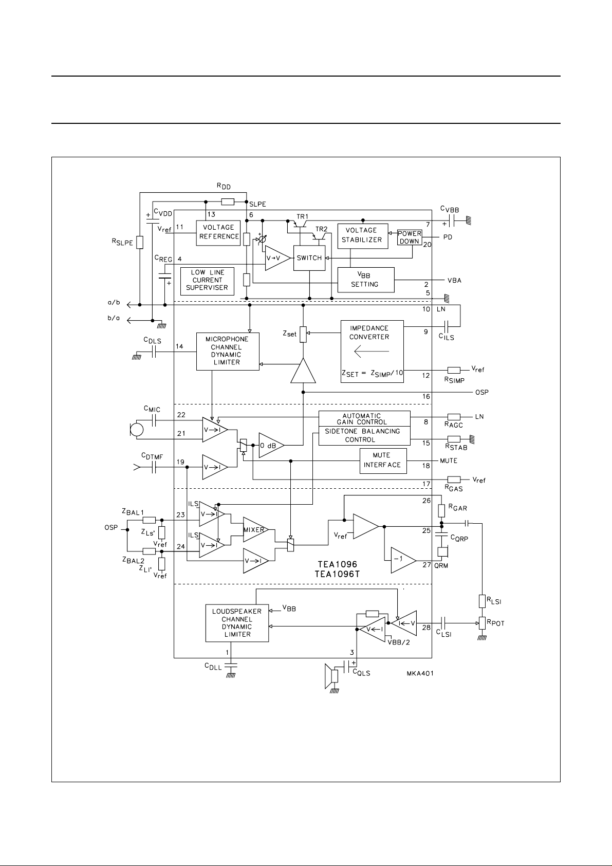
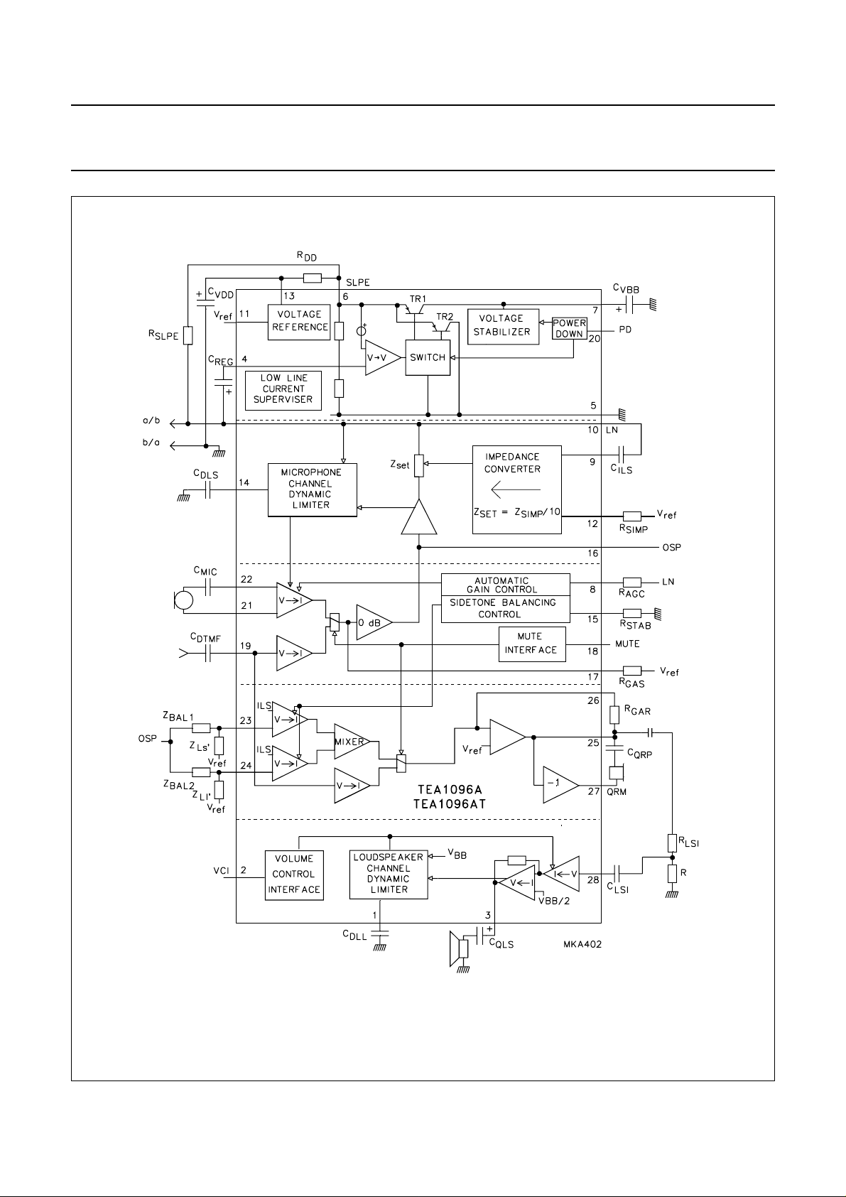
BLOCK DIAGRAMS
Fig.1 Block diagram (TEA1096).
November 1994 4
Page 5
Philips Semiconductors Product Specification
Speech and listening-in IC TEA1096; TEA1096A
Fig.2 Block diagram (TEA1096A).
November 1994 5
Page 6

Philips Semiconductors Product Specification
Speech and listening-in IC TEA1096; TEA1096A
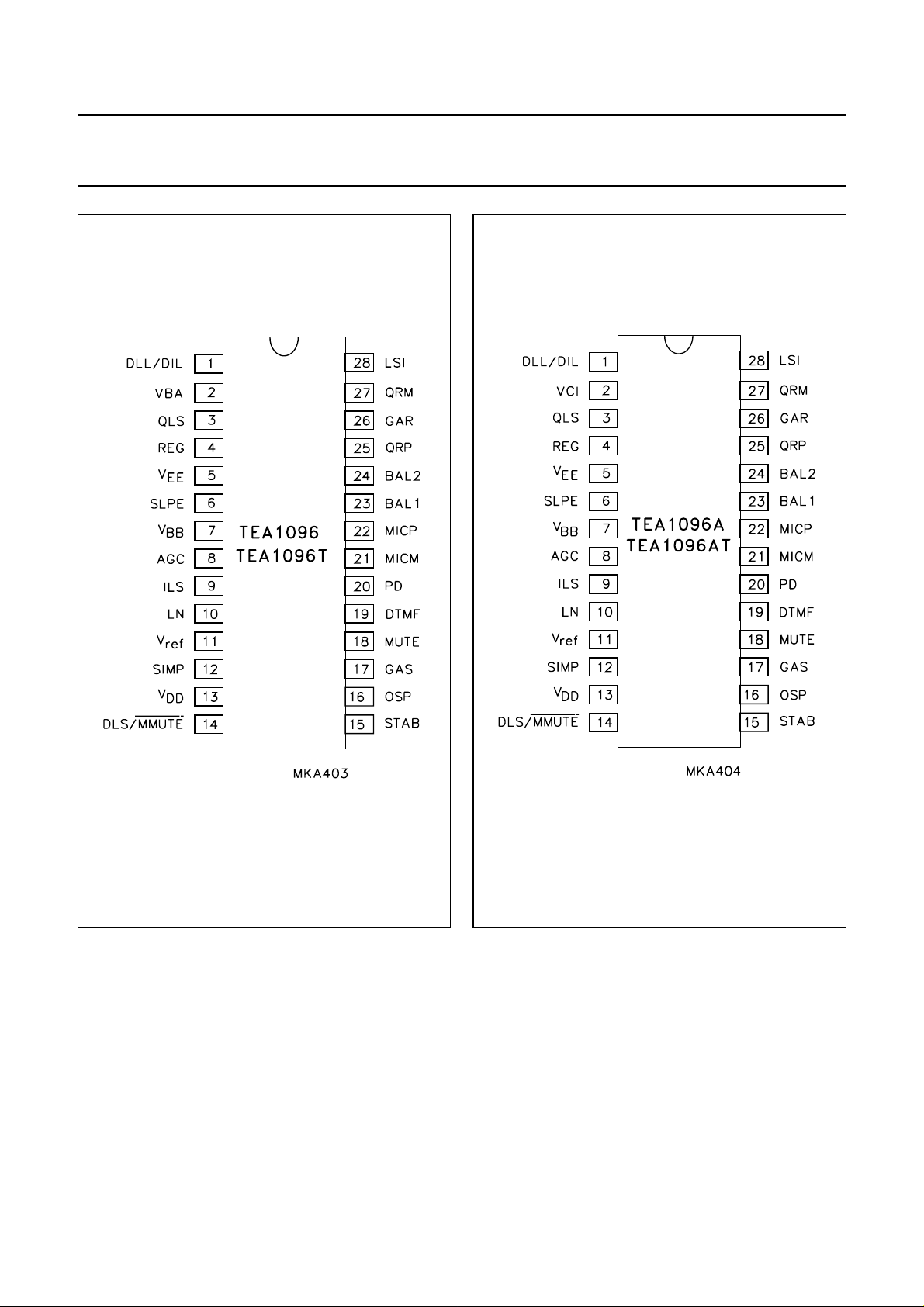
PINNING
SYMBOL
DESCRIPTION
TEA1096 TEA1096A
DLL/DIL 1 1 dynamic limiter and disable input for loudspeaker amplifier
VBA 2 − VBB voltage adjustment
VCI − 2 volume control input for loudspeaker amplifier
QLS 3 3 loudspeaker amplifier output
REG 4 4 decoupling line voltage stabilizer
PINS
V
EE
5 5 negative line terminal (ground reference)
SLPE 6 6 stabilized voltage, connection for slope resistor
V
BB
7 7 stabilized supply voltage for listening-in circuitry
AGC 8 8 automatic gain control
ILS 9 9 input line signal
LN 10 10 positive line terminal
V
ref
11 11 reference voltage output
SIMP 12 12 set impedance input
V
DD
DLS/
MMUTE 14 14 dynamic limiter for sending and microphone mute
13 13 supply voltage for speech circuitry/peripherals
STAB 15 15 reference current adjustment
OSP 16 16 sending preamplifier output
GAS 17 17 sending gain adjustment
MUTE 18 18 mute input to select speech or DTMF dialling
DTMF 19 19 dual-tone multi-frequency (DTMF) input
PD 20 20 power-down input
MICM 21 21 inverting microphone amplifier input
MICP 22 22 non-inverting microphone amplifier input
BAL1 23 23 connection for balance network 1
BAL2 24 24 connection for balance network 2
QRP 25 25 non-inverting receiving amplifier output
GAR 26 26 receiving gain adjustment
QRM 27 27 inverting receiving amplifier output
LSI 28 28 loudspeaker amplifier input
November 1994 6
Page 7
Philips Semiconductors Product Specification
Speech and listening-in IC TEA1096; TEA1096A
Fig.3 Pin configuration (TEA1096).
November 1994 7
Fig.4 Pin configuration (TEA1096A).
Page 8
Philips Semiconductors Product Specification
Speech and listening-in IC TEA1096; TEA1096A
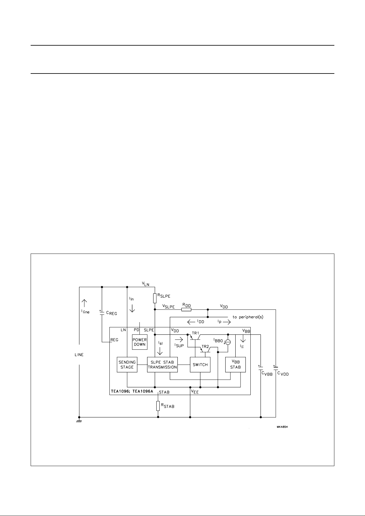
FUNCTIONAL DESCRIPTION
Remark: all data given in this chapter are typical values
except when otherwise specified.
Supply pins SLPE, LN, V
, VBB, VDD, REG and PD
EE
The supply for the TEA1096/TEA1096A and its
peripherals is obtained from the telephone line. The
circuits regulate the line voltage and generate their own
supply voltages V
and VBB to power the transmission
DD
part and the loudspeaker amplifier respectively.
As can be seen from Fig.5, the line current (I
) is split
line
between the sending output stage (Iln), the circuitry
connected to SLPE (Isl), the transmission circuit (IDD), the
peripheral circuits (Ip) and the current switch (I
SUP
). It can
be shown that:
I
SUP=Iline
− (Iln+Isl+IDD+IP)
With nominal conditions where:
Iln= 5 mA, Isl= 0.3 mA and IDD= 2.4 mA
it therefore follows that I
SUP
≈ I
− 7.7 mA − IP.
line
The remaining current I
part. The current consumption I
is available for the listening-in
SUP
of the listening-in
BB0
circuitry is 2.5 mA. To power the loudspeaker, the line
current has to be more than 10 mA.
The voltage at SLPE is stabilized at 4.45 V nominal. The
DC line voltage is regulated at:
VLN=V
SLPE+RSLPE
× (I
line
− Iln).
The supply voltage for the transmission part and
peripheral circuits (VDD) is generated from V
equal to VDD=V
− RDD× (IDD+Ip).
SLPE
SLPE
and is
VBB supplies the listening-in circuitry and is stabilized at
3.6 V nominal.
A resistor connected between pin REG and VEE can be
used to decrease the SLPE voltage while maintaining V
BB
at its nominal value, whereas a resistor connected
between pin REG and pin SLPE will increase the SLPE
voltage while maintaining VBB at its nominal value. When
adjusting the SLPE voltage to a lower value, care should
be taken that the V
is at least 0.4 V higher than V
SLPE
BB
(VBB supply efficiency).
Fig.5 Supply arrangement.
November 1994 8
Page 9
Philips Semiconductors Product Specification
Speech and listening-in IC TEA1096; TEA1096A
The function of the current switch TR1-TR2 is to reduce
distortion of large line signals. Current I
VBB via TR1, when V
V
is lower, this current is shunted to VEE via TR2. All
SLPE
is higher than VBB+ 0.4 V. When
SLPE
is supplied to
SUP
excess line current, not used for internal supply is
consumed in the VBB stabilizer or directly shunted to VEE.
To reduce the current consumption during pulse dialling,
the TEA1096/TEA1096A are provided with a power-down
(PD) input. The PD input has a pull-down structure. When
the voltage on PD is HIGH, the current consumption from
VDD capacitor C
point 350 µA. The capacitors C
is 100 µA and from the VBB supply
VDD
(100 µF) and C
VDD
VBB
(470 µF) are sufficient to power theTEA1096/TEA1096A
during pulse dialling/flash.
V
voltage adjustment: pin VBA (TEA1096 only)
BB
A resistor connected between pins VBA and V
can be
EE
used to increase the VBB voltage, whereas a resistor
connected between pins VBA and VBB will decrease the
VBB voltage. When adjusting the VBB voltage to a higher
value, care should be taken that V
is at least 0.4 V
SLPE
higher than VBB (VBB supply efficiency).
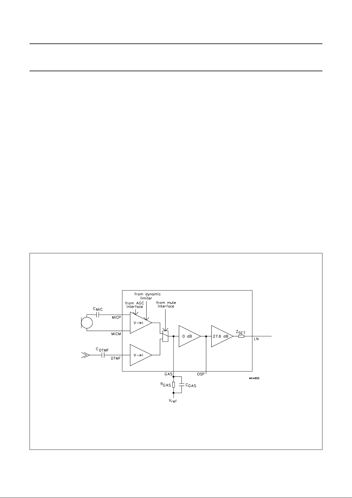
Sending channel: pins MICP, MICM, DTMF, GAS, OSP, LN, MUTE, DLS and AGC
The TEA1096/TEA1096A has symmetrical microphone
inputs MICP, MICM with an input resistance of 64 kΩ
between MICP and MICM (2 × 32 kΩ). In the speech mode
(MUTE = LOW), the overall gain from MICP-MICM to LN
can be adjusted from 33 dB to 52 dB to suit specific
requirements. The gain is proportional to the value of R
and equals 52 dB with R
capacitor C
connected in parallel with R
GAS
= 90.9 kΩ and I
GAS
= 20 mA. A
line
GAS
GAS
can be
used to provide a first-order low-pass filter.
Automatic gain control (AGC) is provided for line-loss
compensation as well as dynamic limitation for reduction
of the distortion of the transmitted signal on the line. The
microphone amplifier can be disabled by short-circuiting
pin DLS to VEE (secret function) and can be muted into
DTMF mode by applying a HIGH level on pin MUTE.
The TEA1096/TEA1096A has an asymmetrical DTMF
input with an input resistance of 20 kΩ. In the DTMF mode,
the overall gain from DTMF to LN is proportional to R
GAS
and is 26.5 dB less than the microphone amplifier gain.
Switch-over from one mode to the other is click-free.
,
Fig.6 Sending channel.
November 1994 9
Page 10
Philips Semiconductors Product Specification
Speech and listening-in IC TEA1096; TEA1096A
It can be calculated from Fig.7 that the AC modulator gain
can be written:
V
LN
• providing
-------------V
OSP
Z
SET=Zline
-----------------------------------------------------( Z
Z
line
Z
line
SET
) 24×+
12==
• Gv (LN to OSP) = 21.6 dB.
The frequency response for audio frequencies of the
sending channel is flat in this case for a complex line
termination.
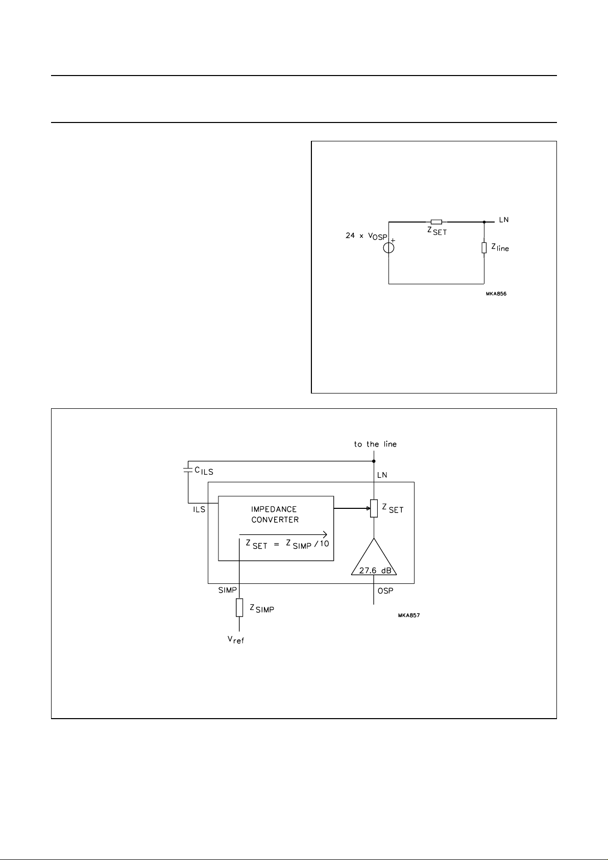
Set impedance: pins ILS, SIMP and LN
The TEA1096/TEA1096A provides an active set
impedance in both the receiving and sending conditions,
thus allowing a flat frequency response for a complex line
impedance, without the need for any extra compensation
network.
As can be derived from Fig.8 the set impedance Z
10 times lower than Z
SIMP
.
SET
is
Fig.7 AC modulator equivalent model.
Fig.8 Set impedance.
November 1994 10
Page 11

Philips Semiconductors Product Specification
Speech and listening-in IC TEA1096; TEA1096A
Fig.9 Equivalent AC impedance between LN and VEE.
The equivalent impedance connected between LN and
VEE is illustrated in Fig.9.
Where:
• LEQ=REQ× C
REG
× R
SLPE
• REQ=40kΩ
• Z
SET
=1⁄10Z
SIMP
.
Remark: a resistor R (REG-VEE) connected between REG
and VEE (to lower the regulated voltage) changes REQ into
REQ// R (REG-VEE), whereas a resistor R
REG-SLPE
connected between REG and SLPE (to increase the
regulated voltage) has no effect on REQ.
Dynamic limiter of the microphone channel: pin DLS
The dynamic limiter in the microphone channel of the
TEA1096/TEA1096A prevents clipping of the microphone
signal, and limits the transmitted signal on LN to a
maximum value of typically 3.65 V (4.4 dBm).
Clipping on the microphone channel is prevented by
rapidly reducing the gain when the output stage starts to
saturate. The time in which the gain reduction is effected
(clipping attack time) is approximately a few milliseconds.
The microphone channel stays in the reduced gain mode
until the peaks of the signal no longer cause saturation.
The gain of the microphone channel then returns to its
normal value within the clipping release time.
Both attack and release time are proportional to the value
of the capacitor C
. The THD (Total Harmonic
DLS
Distortion) of the microphone amplifier in the reduced gain
mode stays below 2% up to 10 dB of input voltage
overdrive [provided that V
MICP
, V
MICM
is below 10 mV
(RMS)].
The dynamic limiter of the TEA1096/TEA1096A also
provides a microphone mute (secret function) when pin
DLS is short-circuited to VEE. The microphone gain is then
80 dB lower. The release time after a microphone mute is
approximately 10 ms.
November 1994 11
Page 12

Philips Semiconductors Product Specification
Speech and listening-in IC TEA1096; TEA1096A
Fig.10 Dynamic limiter of the microphone channel.
Receiving amplifier: pins LN, GAR, QRP and QRM
The receiver gain is defined between the line connection
LN and the earpiece complementary outputs QRP
(non-inverting) and QRM (inverting). With R
GAR
equal to
90.9 kΩ the gain from LN to QRP is −2.5 dB. The outputs
may be used to connect a dynamic, magnetic or
piezoelectric earpiece. When the earpiece impedance
exceeds 450 Ω, differential drive (BTL connection) can be
used. As both outputs are in opposite phase, the gain from
LN to QRP or QRM is 3.5 dB.
By means of the R
resistor, the gain of the receiving
GAR
amplifier can be adjusted to suit the sensitivity of the
transducer which is used. The permitted range is between
−14 dB and +6 dB for single-ended drive (SE), and
between −8 dB and +12 dB for bridge-tied load (BTL)
drive.
Two external capacitors, C
ensure stability. The C
GAR
(100 pF) and C
GAR
GARS
(1 nF),
capacitor is also used to obtain
a first-order low-pass filter. The cut-off frequency
(corresponding to the time constant R
adjusted by the C
C
GARS=CGAR
capacitor, but the relationship
GAR
× 10 must be maintained.
GAR
× C
GAR
) can be
During DTMF dialling, the dialling tones can be heard in
the earpiece at a very low level. This is called confidence
tone.
Automatic gain control: pin AGC
Automatic compensation of line-loss is obtained by
connecting a resistor R
between pin LN and pin AGC.
AGC
This automatic gain control changes the gain of the
microphone and receiving amplifiers in accordance with
the DC line current.
The control range is 6 dB; This corresponds to a 5 km line
of 0.5 mm diameter copper twisted-pair cable:
DC resistance = 176 Ω /km
average attenuation = 1.2 dB/km.
The value of R
must be chosen with reference to the
AGC
exchange supply voltage and its feeding bridge resistance
and has no influence on the ratio (I
start/Istop
) which remains
constant. Figure11 illustrates the gain attenuation when
R
= 100 kΩ. If automatic line-loss compensation is not
AGC
required, the AGC pin can be left open circuit, the
amplifiers then give their maximum gain and the double
sidetone principle is no longer active. Only one network is
used. Pins BAL1 and BAL2 must then be short-circuited
together.
November 1994 12
Page 13

Philips Semiconductors Product Specification
BBBBBBBBBBBBBBBBBBBBBBBBBBBBBBBBBBBBBBBBBBBBBBBBBBBBBBBBBBBBBBBBBBBBBBBBBBBBBBBBBBBBBBBBBBBBBBBBBBBBBBBBBBBBBBBBB
B
B
B
B
B
B
B
B
B
B
B
B
B
B
B
B
B
B
B
B
B
B
B
B
B
B
B
B
B
B
B
B
B
B
B
B
B
B
B
B
B
B
B
B
B
B
B
B
B
B
B
B
B
B
B
B
B
B
B
B
B
B
B
B
B
B
B
B
B
B
B
B
B
B
B
BBBBBBBBBBBBBBBBBBBBBBBBBBBBBBBBBBBBBBBBBBBBBBBBBBBBBBBBBBBBBBBBBBBBBBBBBBBBBBBBBBBBBBBBBBBBBBBBBBBBBBBBBBBBBBBBB
Speech and listening-in IC TEA1096; TEA1096A
BBBBBBBBBBBBBBBBBBBBBBBBBBBBBBBBBBBBBBBBBBBBBBBBBBBBBBBBBBBBBBBBBBBBBBBBBBBBBBBBBBBBBBBBBBBBBBBBBBBBBBBBBBBBBBBB
BBBBBBBBBBBBBBBBBBBBBBBBBBBBBBBBBBBBBBBBBBBBBBBBBBBBBBBBBBBBBBBBBBBBBBBBBBBBBBBBBBBBBBBBBBBBBBBBBBBBBBBBBBBBBBBB
BBBBBBBBBBBBBBBBBBBBBBBBBBBBBBBBBBBBBBBBBBBBBBBBBBBBBBBBBBBBBBBBBBBBBBBBBBBBBBBBBBBBBBBBBBBBBBBBBBBBBBBBBBBBBBBB
BBBBBBBBBBBBBBBBBBBBBBBBBBBBBBBBBBBBBBBBBBBBBBBBBBBBBBBBBBBBBBBBBBBBBBBBBBBBBBBBBBBBBBBBBBBBBBBBBBBBBBBBBBBBBBBB
BBBBBBBBBBBBBBBBBBBBBBBBBBBBBBBBBBBBBBBBBBBBBBBBBBBBBBBBBBBBBBBBBBBBBBBBBBBBBBBBBBBBBBBBBBBBBBBBBBBBBBBBBBBBBBBB
BBBBBBBBBBBBBBBBBBBBBBBBBBBBBBBBBBBBBBBBBBBBBBBBBBBBBBBBBBBBBBBBBBBBBBBBBBBBBBBBBBBBBBBBBBBBBBBBBBBBBBBBBBBBBBBB
BBBBBBBBBBBBBBBBBBBBBBBBBBBBBBBBBBBBBBBBBBBBBBBBBBBBBBBBBBBBBBBBBBBBBBBBBBBBBBBBBBBBBBBBBBBBBBBBBBBBBBBBBBBBBBBB
BBBBBBBBBBBBBBBBBBBBBBBBBBBBBBBBBBBBBBBBBBBBBBBBBBBBBBBBBBBBBBBBBBBBBBBBBBBBBBBBBBBBBBBBBBBBBBBBBBBBBBBBBBBBBBBB
BBBBBBBBBBBBBBBBBBBBBBBBBBBBBBBBBBBBBBBBBBBBBBBBBBBBBBBBBBBBBBBBBBBBBBBBBBBBBBBBBBBBBBBBBBBBBBBBBBBBBBBBBBBBBBBB
BBBBBBBBBBBBBBBBBBBBBBBBBBBBBBBBBBBBBBBBBBBBBBBBBBBBBBBBBBBBBBBBBBBBBBBBBBBBBBBBBBBBBBBBBBBBBBBBBBBBBBBBBBBBBBBB
BBBBBBBBBBBBBBBBBBBBBBBBBBBBBBBBBBBBBBBBBBBBBBBBBBBBBBBBBBBBBBBBBBBBBBBBBBBBBBBBBBBBBBBBBBBBBBBBBBBBBBBBBBBBBBBB
BBBBBBBBBBBBBBBBBBBBBBBBBBBBBBBBBBBBBBBBBBBBBBBBBBBBBBBBBBBBBBBBBBBBBBBBBBBBBBBBBBBBBBBBBBBBBBBBBBBBBBBBBBBBBBBB
BBBBBBBBBBBBBBBBBBBBBBBBBBBBBBBBBBBBBBBBBBBBBBBBBBBBBBBBBBBBBBBBBBBBBBBBBBBBBBBBBBBBBBBBBBBBBBBBBBBBBBBBBBBBBBBB
BBBBBBBBBBBBBBBBBBBBBBBBBBBBBBBBBBBBBBBBBBBBBBBBBBBBBBBBBBBBBBBBBBBBBBBBBBBBBBBBBBBBBBBBBBBBBBBBBBBBBBBBBBBBBBBB
BBBBBBBBBBBBBBBBBBBBBBBBBBBBBBBBBBBBBBBBBBBBBBBBBBBBBBBBBBBBBBBBBBBBBBBBBBBBBBBBBBBBBBBBBBBBBBBBBBBBBBBBBBBBBBBB
BBBBBBBBBBBBBBBBBBBBBBBBBBBBBBBBBBBBBBBBBBBBBBBBBBBBBBBBBBBBBBBBBBBBBBBBBBBBBBBBBBBBBBBBBBBBBBBBBBBBBBBBBBBBBBBB
BBBBBBBBBBBBBBBBBBBBBBBBBBBBBBBBBBBBBBBBBBBBBBBBBBBBBBBBBBBBBBBBBBBBBBBBBBBBBBBBBBBBBBBBBBBBBBBBBBBBBBBBBBBBBBBB
BBBBBBBBBBBBBBBBBBBBBBBBBBBBBBBBBBBBBBBBBBBBBBBBBBBBBBBBBBBBBBBBBBBBBBBBBBBBBBBBBBBBBBBBBBBBBBBBBBBBBBBBBBBBBBBB
BBBBBBBBBBBBBBBBBBBBBBBBBBBBBBBBBBBBBBBBBBBBBBBBBBBBBBBBBBBBBBBBBBBBBBBBBBBBBBBBBBBBBBBBBBBBBBBBBBBBBBBBBBBBBBBB
BBBBBBBBBBBBBBBBBBBBBBBBBBBBBBBBBBBBBBBBBBBBBBBBBBBBBBBBBBBBBBBBBBBBBBBBBBBBBBBBBBBBBBBBBBBBBBBBBBBBBBBBBBBBBBBB
BBBBBBBBBBBBBBBBBBBBBBBBBBBBBBBBBBBBBBBBBBBBBBBBBBBBBBBBBBBBBBBBBBBBBBBBBBBBBBBBBBBBBBBBBBBBBBBBBBBBBBBBBBBBBBBB
BBBBBBBBBBBBBBBBBBBBBBBBBBBBBBBBBBBBBBBBBBBBBBBBBBBBBBBBBBBBBBBBBBBBBBBBBBBBBBBBBBBBBBBBBBBBBBBBBBBBBBBBBBBBBBBB
BBBBBBBBBBBBBBBBBBBBBBBBBBBBBBBBBBBBBBBBBBBBBBBBBBBBBBBBBBBBBBBBBBBBBBBBBBBBBBBBBBBBBBBBBBBBBBBBBBBBBBBBBBBBBBBB
BBBBBBBBBBBBBBBBBBBBBBBBBBBBBBBBBBBBBBBBBBBBBBBBBBBBBBBBBBBBBBBBBBBBBBBBBBBBBBBBBBBBBBBBBBBBBBBBBBBBBBBBBBBBBBBB
BBBBBBBBBBBBBBBBBBBBBBBBBBBBBBBBBBBBBBBBBBBBBBBBBBBBBBBBBBBBBBBBBBBBBBBBBBBBBBBBBBBBBBBBBBBBBBBBBBBBBBBBBBBBBBBB
BBBBBBBBBBBBBBBBBBBBBBBBBBBBBBBBBBBBBBBBBBBBBBBBBBBBBBBBBBBBBBBBBBBBBBBBBBBBBBBBBBBBBBBBBBBBBBBBBBBBBBBBBBBBBBBB
BBBBBBBBBBBBBBBBBBBBBBBBBBBBBBBBBBBBBBBBBBBBBBBBBBBBBBBBBBBBBBBBBBBBBBBBBBBBBBBBBBBBBBBBBBBBBBBBBBBBBBBBBBBBBBBB
BBBBBBBBBBBBBBBBBBBBBBBBBBBBBBBBBBBBBBBBBBBBBBBBBBBBBBBBBBBBBBBBBBBBBBBBBBBBBBBBBBBBBBBBBBBBBBBBBBBBBBBBBBBBBBBB
BBBBBBBBBBBBBBBBBBBBBBBBBBBBBBBBBBBBBBBBBBBBBBBBBBBBBBBBBBBBBBBBBBBBBBBBBBBBBBBBBBBBBBBBBBBBBBBBBBBBBBBBBBBBBBBB
BBBBBBBBBBBBBBBBBBBBBBBBBBBBBBBBBBBBBBBBBBBBBBBBBBBBBBBBBBBBBBBBBBBBBBBBBBBBBBBBBBBBBBBBBBBBBBBBBBBBBBBBBBBBBBBB
BBBBBBBBBBBBBBBBBBBBBBBBBBBBBBBBBBBBBBBBBBBBBBBBBBBBBBBBBBBBBBBBBBBBBBBBBBBBBBBBBBBBBBBBBBBBBBBBBBBBBBBBBBBBBBBB
BBBBBBBBBBBBBBBBBBBBBBBBBBBBBBBBBBBBBBBBBBBBBBBBBBBBBBBBBBBBBBBBBBBBBBBBBBBBBBBBBBBBBBBBBBBBBBBBBBBBBBBBBBBBBBBB
BBBBBBBBBBBBBBBBBBBBBBBBBBBBBBBBBBBBBBBBBBBBBBBBBBBBBBBBBBBBBBBBBBBBBBBBBBBBBBBBBBBBBBBBBBBBBBBBBBBBBBBBBBBBBBBB
BBBBBBBBBBBBBBBBBBBBBBBBBBBBBBBBBBBBBBBBBBBBBBBBBBBBBBBBBBBBBBBBBBBBBBBBBBBBBBBBBBBBBBBBBBBBBBBBBBBBBBBBBBBBBBBB
BBBBBBBBBBBBBBBBBBBBBBBBBBBBBBBBBBBBBBBBBBBBBBBBBBBBBBBBBBBBBBBBBBBBBBBBBBBBBBBBBBBBBBBBBBBBBBBBBBBBBBBBBBBBBBBB
BBBBBBBBBBBBBBBBBBBBBBBBBBBBBBBBBBBBBBBBBBBBBBBBBBBBBBBBBBBBBBBBBBBBBBBBBBBBBBBBBBBBBBBBBBBBBBBBBBBBBBBBBBBBBBBB
BBBBBBBBBBBBBBBBBBBBBBBBBBBBBBBBBBBBBBBBBBBBBBBBBBBBBBBBBBBBBBBBBBBBBBBBBBBBBBBBBBBBBBBBBBBBBBBBBBBBBBBBBBBBBBBB
BBBBBBBBBBBBBBBBBBBBBBBBBBBBBBBBBBBBBBBBBBBBBBBBBBBBBBBBBBBBBBBBBBBBBBBBBBBBBBBBBBBBBBBBBBBBBBBBBBBBBBBBBBBBBBBB
BBBBBBBBBBBBBBBBBBBBBBBBBBBBBBBBBBBBBBBBBBBBBBBBBBBBBBBBBBBBBBBBBBBBBBBBBBBBBBBBBBBBBBBBBBBBBBBBBBBBBBBBBBBBBBBB
BBBBBBBBBBBBBBBBBBBBBBBBBBBBBBBBBBBBBBBBBBBBBBBBBBBBBBBBBBBBBBBBBBBBBBBBBBBBBBBBBBBBBBBBBBBBBBBBBBBBBBBBBBBBBBBB
BBBBBBBBBBBBBBBBBBBBBBBBBBBBBBBBBBBBBBBBBBBBBBBBBBBBBBBBBBBBBBBBBBBBBBBBBBBBBBBBBBBBBBBBBBBBBBBBBBBBBBBBBBBBBBBB
BBBBBBBBBBBBBBBBBBBBBBBBBBBBBBBBBBBBBBBBBBBBBBBBBBBBBBBBBBBBBBBBBBBBBBBBBBBBBBBBBBBBBBBBBBBBBBBBBBBBBBBBBBBBBBBB
BBBBBBBBBBBBBBBBBBBBBBBBBBBBBBBBBBBBBBBBBBBBBBBBBBBBBBBBBBBBBBBBBBBBBBBBBBBBBBBBBBBBBBBBBBBBBBBBBBBBBBBBBBBBBBBB
BBBBBBBBBBBBBBBBBBBBBBBBBBBBBBBBBBBBBBBBBBBBBBBBBBBBBBBBBBBBBBBBBBBBBBBBBBBBBBBBBBBBBBBBBBBBBBBBBBBBBBBBBBBBBBBB
BBBBBBBBBBBBBBBBBBBBBBBBBBBBBBBBBBBBBBBBBBBBBBBBBBBBBBBBBBBBBBBBBBBBBBBBBBBBBBBBBBBBBBBBBBBBBBBBBBBBBBBBBBBBBBBB
BBBBBBBBBBBBBBBBBBBBBBBBBBBBBBBBBBBBBBBBBBBBBBBBBBBBBBBBBBBBBBBBBBBBBBBBBBBBBBBBBBBBBBBBBBBBBBBBBBBBBBBBBBBBBBBB
BBBBBBBBBBBBBBBBBBBBBBBBBBBBBBBBBBBBBBBBBBBBBBBBBBBBBBBBBBBBBBBBBBBBBBBBBBBBBBBBBBBBBBBBBBBBBBBBBBBBBBBBBBBBBBBB
BBBBBBBBBBBBBBBBBBBBBBBBBBBBBBBBBBBBBBBBBBBBBBBBBBBBBBBBBBBBBBBBBBBBBBBBBBBBBBBBBBBBBBBBBBBBBBBBBBBBBBBBBBBBBBBB
BBBBBBBBBBBBBBBBBBBBBBBBBBBBBBBBBBBBBBBBBBBBBBBBBBBBBBBBBBBBBBBBBBBBBBBBBBBBBBBBBBBBBBBBBBBBBBBBBBBBBBBBBBBBBBBB
BBBBBBBBBBBBBBBBBBBBBBBBBBBBBBBBBBBBBBBBBBBBBBBBBBBBBBBBBBBBBBBBBBBBBBBBBBBBBBBBBBBBBBBBBBBBBBBBBBBBBBBBBBBBBBBB
BBBBBBBBBBBBBBBBBBBBBBBBBBBBBBBBBBBBBBBBBBBBBBBBBBBBBBBBBBBBBBBBBBBBBBBBBBBBBBBBBBBBBBBBBBBBBBBBBBBBBBBBBBBBBBBB
BBBBBBBBBBBBBBBBBBBBBBBBBBBBBBBBBBBBBBBBBBBBBBBBBBBBBBBBBBBBBBBBBBBBBBBBBBBBBBBBBBBBBBBBBBBBBBBBBBBBBBBBBBBBBBBB
BBBBBBBBBBBBBBBBBBBBBBBBBBBBBBBBBBBBBBBBBBBBBBBBBBBBBBBBBBBBBBBBBBBBBBBBBBBBBBBBBBBBBBBBBBBBBBBBBBBBBBBBBBBBBBBB
BBBBBBBBBBBBBBBBBBBBBBBBBBBBBBBBBBBBBBBBBBBBBBBBBBBBBBBBBBBBBBBBBBBBBBBBBBBBBBBBBBBBBBBBBBBBBBBBBBBBBBBBBBBBBBBB
BBBBBBBBBBBBBBBBBBBBBBBBBBBBBBBBBBBBBBBBBBBBBBBBBBBBBBBBBBBBBBBBBBBBBBBBBBBBBBBBBBBBBBBBBBBBBBBBBBBBBBBBBBBBBBBB
BBBBBBBBBBBBBBBBBBBBBBBBBBBBBBBBBBBBBBBBBBBBBBBBBBBBBBBBBBBBBBBBBBBBBBBBBBBBBBBBBBBBBBBBBBBBBBBBBBBBBBBBBBBBBBBB
BBBBBBBBBBBBBBBBBBBBBBBBBBBBBBBBBBBBBBBBBBBBBBBBBBBBBBBBBBBBBBBBBBBBBBBBBBBBBBBBBBBBBBBBBBBBBBBBBBBBBBBBBBBBBBBB
BBBBBBBBBBBBBBBBBBBBBBBBBBBBBBBBBBBBBBBBBBBBBBBBBBBBBBBBBBBBBBBBBBBBBBBBBBBBBBBBBBBBBBBBBBBBBBBBBBBBBBBBBBBBBBBB
BBBBBBBBBBBBBBBBBBBBBBBBBBBBBBBBBBBBBBBBBBBBBBBBBBBBBBBBBBBBBBBBBBBBBBBBBBBBBBBBBBBBBBBBBBBBBBBBBBBBBBBBBBBBBBBB
BBBBBBBBBBBBBBBBBBBBBBBBBBBBBBBBBBBBBBBBBBBBBBBBBBBBBBBBBBBBBBBBBBBBBBBBBBBBBBBBBBBBBBBBBBBBBBBBBBBBBBBBBBBBBBBB
BBBBBBBBBBBBBBBBBBBBBBBBBBBBBBBBBBBBBBBBBBBBBBBBBBBBBBBBBBBBBBBBBBBBBBBBBBBBBBBBBBBBBBBBBBBBBBBBBBBBBBBBBBBBBBBB
BBBBBBBBBBBBBBBBBBBBBBBBBBBBBBBBBBBBBBBBBBBBBBBBBBBBBBBBBBBBBBBBBBBBBBBBBBBBBBBBBBBBBBBBBBBBBBBBBBBBBBBBBBBBBBBB
BBBBBBBBBBBBBBBBBBBBBBBBBBBBBBBBBBBBBBBBBBBBBBBBBBBBBBBBBBBBBBBBBBBBBBBBBBBBBBBBBBBBBBBBBBBBBBBBBBBBBBBBBBBBBBBB
BBBBBBBBBBBBBBBBBBBBBBBBBBBBBBBBBBBBBBBBBBBBBBBBBBBBBBBBBBBBBBBBBBBBBBBBBBBBBBBBBBBBBBBBBBBBBBBBBBBBBBBBBBBBBBBB
BBBBBBBBBBBBBBBBBBBBBBBBBBBBBBBBBBBBBBBBBBBBBBBBBBBBBBBBBBBBBBBBBBBBBBBBBBBBBBBBBBBBBBBBBBBBBBBBBBBBBBBBBBBBBBBB
BBBBBBBBBBBBBBBBBBBBBBBBBBBBBBBBBBBBBBBBBBBBBBBBBBBBBBBBBBBBBBBBBBBBBBBBBBBBBBBBBBBBBBBBBBBBBBBBBBBBBBBBBBBBBBBB
BBBBBBBBBBBBBBBBBBBBBBBBBBBBBBBBBBBBBBBBBBBBBBBBBBBBBBBBBBBBBBBBBBBBBBBBBBBBBBBBBBBBBBBBBBBBBBBBBBBBBBBBBBBBBBBB
BBBBBBBBBBBBBBBBBBBBBBBBBBBBBBBBBBBBBBBBBBBBBBBBBBBBBBBBBBBBBBBBBBBBBBBBBBBBBBBBBBBBBBBBBBBBBBBBBBBBBBBBBBBBBBBB
BBBBBBBBBBBBBBBBBBBBBBBBBBBBBBBBBBBBBBBBBBBBBBBBBBBBBBBBBBBBBBBBBBBBBBBBBBBBBBBBBBBBBBBBBBBBBBBBBBBBBBBBBBBBBBBB
BBBBBBBBBBBBBBBBBBBBBBBBBBBBBBBBBBBBBBBBBBBBBBBBBBBBBBBBBBBBBBBBBBBBBBBBBBBBBBBBBBBBBBBBBBBBBBBBBBBBBBBBBBBBBBBB
BBBBBBBBBBBBBBBBBBBBBBBBBBBBBBBBBBBBBBBBBBBBBBBBBBBBBBBBBBBBBBBBBBBBBBBBBBBBBBBBBBBBBBBBBBBBBBBBBBBBBBBBBBBBBBBB
BBBBBBBBBBBBBBBBBBBBBBBBBBBBBBBBBBBBBBBBBBBBBBBBBBBBBBBBBBBBBBBBBBBBBBBBBBBBBBBBBBBBBBBBBBBBBBBBBBBBBBBBBBBBBBBB
BBBBBBBBBBBBBBBBBBBBBBBBBBBBBBBBBBBBBBBBBBBBBBBBBBBBBBBBBBBBBBBBBBBBBBBBBBBBBBBBBBBBBBBBBBBBBBBBBBBBBBBBBBBBBBBB
BBBBBBBBBBBBBBBBBBBBBBBBBBBBBBBBBBBBBBBBBBBBBBBBBBBBBBBBBBBBBBBBBBBBBBBBBBBBBBBBBBBBBBBBBBBBBBBBBBBBBBBBBBBBBBBB
BBBBBBBBBBBBBBBBBBBBBBBBBBBBBBBBBBBBBBBBBBBBBBBBBBBBBBBBBBBBBBBBBBBBBBBBBBBBBBBBBBBBBBBBBBBBBBBBBBBBBBBBBBBBBBBB
Fig.11 Variation of microphone and receiver gain as a function of the exchange
supply voltage with R
as a parameter.
AGC
Sidetone suppression: pins BAL1, BAL2, OSP and ILS
Suppression of the microphone signal in the earpiece is
obtained by subtracting a part of this signal to a fraction of
the line signal (see Fig.12). For optimum suppression, the
voltage at the BAL inputs (BAL1 and BAL2) should be
equal to:
V
BAL
Z
line
× V
0.5
------------------------------Z
×
SETZline
×=
SOP
To reach this requirement, an anti-sidetone network using
two impedances Z
BAL
and Z
is needed.
LI'
Where: R
where α is a scale factor allowing to have R
of 10 kΩ (DC biasing to V
and BAL2).
In the event of complex impedances, the equivalent
network Zs, representing Z
Zp in accordance with Fig.14.
The components of Zp, scaled by a factor α, are applied in
anti-sidetone network Z
network is shown in Fig.15.
= α×R
LI'
and R
line
BAL
has to be ensured on BAL1
ref
, has to be transformed into
line
. The complete anti-sidetone
LI'
In the event of real impedances, the anti-sidetone network
is composed of resistors connected as shown in Fig.13.
November 1994 13
= α×R
SET
;
LI'
in the order
Page 14

Philips Semiconductors Product Specification
B
Speech and listening-in IC TEA1096; TEA1096A
B
Fig.12 Balance networks connection.
(a) Series impedance (Zs).
(b) Parallel impedance (Zp).
Fig.13 Anti-sidetone network. Fig.14 Equivalent network.
November 1994 14
Page 15

Philips Semiconductors Product Specification
Speech and listening-in IC TEA1096; TEA1096A
Switching from one network to the other is carried out
continuously with the line current, when the R
is connected. When the R
resistor is not connected,
AGC
switching from one network to the other is not possible
(see automatic gain control). Only one network has then to
be applied.
It is also possible to use only one anti-sidetone network. In
this event, both inputs BAL1 and BAL2 must be
short-circuited.
Loudspeaker amplifier: pins LSI and QLS
The loudspeaker amplifier has an asymmetrical input LSI
which is referenced to an internal voltage reference of
1.25 V via an internal resistance of 10 kΩ. The input signal
can be taken from one of the earpiece outputs QRP or
QRM via a potentiometer (R
be chosen in accordance with the gain G
). The attenuation has to
POT
of the receiving
vrx
amplifier.
AGC
resistor
Fig.15 Complete anti-sidetone network.
Again, it means that: Z
Where α is a scale factor allowing Z
10 kΩ (DC biasing to V
= α×Z
LI'
has to be ensured on BAL1 and
ref
and Z
line
to be in the order of
LI'
BAL
= α×Z
SET
BAL2).
As the line impedance Z
varies considerably with the
line
line length, two anti-sidetone networks can be used. One
of them Z
the other one Z
, connected to BAL2 is optimized for long lines,
Ll'
, connected to BAL1 is optimized for
Ls'
short lines:
Where:
Z
Z
Z
Z
Ll'
Ls'
BAL1
BAL2
= α×Z
= α×Z
= α×Z
= α×Z
line
line
(long)
(short)
SET
.
SET
The input stage can handle up to 200 mV (RMS) at room
temperature for 3% of THD.
The gain of the loudspeaker amplifier is fixed at 35.5 dB.
The output QLS is referenced to a DC level of1⁄2VBB to
offer rail-to-rail output swing.
The maximum voltage gain from line to loudspeaker has to
be fixed in relation to the side-tone transfer of the
telephone set. An enlarged listening-in gain improves the
listening-in behaviour but can introduce audible
instabilities in the form of howling during normal use of the
set. The loudspeaker can be disabled by short-circuiting
DLL/DIL input to VEE.
November 1994 15
Page 16

Philips Semiconductors Product Specification
Speech and listening-in IC TEA1096; TEA1096A
Fig.16 Loudspeaker amplifier channel.
Dynamic limiter/loudspeaker amplifier disabling;
pin DLL/DIL
The dynamic limiter in the loudspeaker channel of the
TEA1096/TEA1096A prevents clipping of the loudspeaker
output stage and protects the functioning of the circuit
when low supply conditions are detected.
Hard clipping of the loudspeaker output stage is prevented
by rapidly reducing the gain when the output stage starts
to saturate. The time in which the gain reduction is effected
(clipping attack time) is approximately a few milliseconds.
The loudspeaker amplifier stays in the reduced gain mode
until the peaks of the loudspeaker signals no longer start
to cause saturation. The gain of the loudspeaker amplifier
then returns to its normal value within the clipping release
time. Both attack and release time are proportional to the
value of the capacitor C
amplifier in the reduced gain mode stays below 5% up to
10 dB of input voltage overdrive.
. The THD of the loudspeaker
DLL
When the supply conditions drop below the required level,
the gain of the loudspeaker amplifier is reduced in order to
prevent the device from malfunctioning. When the supply
current drops below the required level, the supply voltage
V
decreases. In this condition, the gain of the
BB
loudspeaker amplifier is reduced slowly (approximately a
few seconds). When the supply voltage continues to
decrease and drops below an internal threshold of 2.8 V,
the gain of the loudspeaker amplifier is rapidly reduced
(approximately 1 ms). After returning to normal supply
conditions, the gain of the loudspeaker amplifier is raised
again.
The dynamic limiter also provides a loudspeaker disable
when pin DLL/DIL is short-circuited to VEE. The
loudspeaker gain is then typically 80 dB lower. The
release time is approximately 10 ms.
November 1994 16
Page 17

Philips Semiconductors Product Specification
Speech and listening-in IC TEA1096; TEA1096A
Fig.17 Dynamic limiter of the listening-in part.
Volume control: pin VCI (TEA1096A only)
The TEA1096A is provided with a volume control input
VCI, to adjust the gain of the loudspeaker channel by
means of a controlled DC voltage. A typical application is
illustrated in Fig.18. A pulse width modulation on a
microcontroller open drain output imposes a DC voltage
on the VCI capacitor:
δ KV
××
K
BB
=
---------------------R1 R2+
R1
Where
with δ = duty cycle and
A typical response is given in Fig.19.
V
=
--------------------------------------
VCI
1 δ 1K–()×–
Fig.18 Digital volume control application.
November 1994 17
Page 18

Philips Semiconductors Product Specification
Speech and listening-in IC TEA1096; TEA1096A
Fig.19 Change of loudspeaker gain as a function of the voltage at VCI.
November 1994 18
Page 19

Philips Semiconductors Product Specification
Speech and listening-in IC TEA1096; TEA1096A
LIMITING VALUES
In accordance with the Absolute Maximum Rating System (IEC 134).
SYMBOLS PARAMETER CONDITIONS MIN. MAX. UNIT
V
V
V
V
V
V
I
P
T
T
LN
DD
BB
n1
n2
n3
line
tot
stg
amb
voltage on pin LN VEE− 0.4 12.0 V
voltage on pin VDD VEE− 0.4 12.0 V
voltage on pin VBB VEE− 0.4 12.0 V
voltage on pins:
VEE− 0.4 VLN+ 0.4 V
REG, SLPE, AGC and ILS
voltage on pins:
VEE− 0.4 VBB+ 0.4 V
DLL, VBA or VCI, QLS, LSI
voltage on pins: V
, SIMP, STAB,
ref
VEE− 0.4 VDD+ 0.4 V
DLS, OSP, GAS, MUTE, DTMF, PD,
MICM, MICP, BAL1, BAL2, QRP,
QRM, GAR
line current see also Figs 20
− 140 mA
and 21
total power dissipation: T
TEA1096/TEA1096A − 0.91 W
= +75 °C;
amb
see Figs 20 and 21
TEA1096T/TEA1096AT − 0.66 W
storage temperature −40 +125 °C
operating ambient temperature −25 +75 °C
THERMAL CHARACTERISTICS
SYMBOLS PARAMETER VALUE UNIT
R
th j-a
thermal resistance from junction to ambient in free air:
TEA1096; TEA1096A 55 K/W
TEA1096T; TEA1096AT (note 1) 75 K/W
Note
1. Mounted on epoxy board 40.1×19.1 × 1.5 mm.
November 1994 19
Page 20

Philips Semiconductors Product Specification
BBBBBBBBBBBBBBBBBBBBBBBBBBBBBBBBBBBBBBBBBBBBBBBBBBBBBBBBBBBBBBBBBBBBBBBBBBBBBBBBBBBBBBB
B
B
B
B
B
B
B
B
B
B
B
B
B
B
B
B
B
B
B
B
B
B
B
B
B
B
B
B
B
B
B
B
B
B
B
B
B
B
B
B
B
B
B
B
B
B
B
B
B
B
B
B
B
B
B
B
B
B
B
B
BBBBBBBBBBBBBBBBBBBBBBBBBBBBBBBBBBBBBBBBBBBBBBBBBBBBBBBBBBBBBBBBBBBBBBBBBBBBBBBBBBBBBBB
Speech and listening-in IC TEA1096; TEA1096A
(1) T
(2) T
(3) T
=55°C; P
amb
=65°C; P
amb
=75°C; P
amb
= 1272 mW.
tot
= 1091 mW.
tot
= 910 mW.
tot
Fig.20 TEA1096; TEA1096A safe operating area.
BBBBBBBBBBBBBBBBBBBBBBBBBBBBBBBBBBBBBBBBBBBBBBBBBBBBBBBBBBBBBBBBBBBBBBBBBBBBBBBBBBBBBB
BBBBBBBBBBBBBBBBBBBBBBBBBBBBBBBBBBBBBBBBBBBBBBBBBBBBBBBBBBBBBBBBBBBBBBBBBBBBBBBBBBBBBB
BBBBBBBBBBBBBBBBBBBBBBBBBBBBBBBBBBBBBBBBBBBBBBBBBBBBBBBBBBBBBBBBBBBBBBBBBBBBBBBBBBBBBB
BBBBBBBBBBBBBBBBBBBBBBBBBBBBBBBBBBBBBBBBBBBBBBBBBBBBBBBBBBBBBBBBBBBBBBBBBBBBBBBBBBBBBB
BBBBBBBBBBBBBBBBBBBBBBBBBBBBBBBBBBBBBBBBBBBBBBBBBBBBBBBBBBBBBBBBBBBBBBBBBBBBBBBBBBBBBB
BBBBBBBBBBBBBBBBBBBBBBBBBBBBBBBBBBBBBBBBBBBBBBBBBBBBBBBBBBBBBBBBBBBBBBBBBBBBBBBBBBBBBB
BBBBBBBBBBBBBBBBBBBBBBBBBBBBBBBBBBBBBBBBBBBBBBBBBBBBBBBBBBBBBBBBBBBBBBBBBBBBBBBBBBBBBB
BBBBBBBBBBBBBBBBBBBBBBBBBBBBBBBBBBBBBBBBBBBBBBBBBBBBBBBBBBBBBBBBBBBBBBBBBBBBBBBBBBBBBB
BBBBBBBBBBBBBBBBBBBBBBBBBBBBBBBBBBBBBBBBBBBBBBBBBBBBBBBBBBBBBBBBBBBBBBBBBBBBBBBBBBBBBB
BBBBBBBBBBBBBBBBBBBBBBBBBBBBBBBBBBBBBBBBBBBBBBBBBBBBBBBBBBBBBBBBBBBBBBBBBBBBBBBBBBBBBB
BBBBBBBBBBBBBBBBBBBBBBBBBBBBBBBBBBBBBBBBBBBBBBBBBBBBBBBBBBBBBBBBBBBBBBBBBBBBBBBBBBBBBB
BBBBBBBBBBBBBBBBBBBBBBBBBBBBBBBBBBBBBBBBBBBBBBBBBBBBBBBBBBBBBBBBBBBBBBBBBBBBBBBBBBBBBB
BBBBBBBBBBBBBBBBBBBBBBBBBBBBBBBBBBBBBBBBBBBBBBBBBBBBBBBBBBBBBBBBBBBBBBBBBBBBBBBBBBBBBB
BBBBBBBBBBBBBBBBBBBBBBBBBBBBBBBBBBBBBBBBBBBBBBBBBBBBBBBBBBBBBBBBBBBBBBBBBBBBBBBBBBBBBB
BBBBBBBBBBBBBBBBBBBBBBBBBBBBBBBBBBBBBBBBBBBBBBBBBBBBBBBBBBBBBBBBBBBBBBBBBBBBBBBBBBBBBB
BBBBBBBBBBBBBBBBBBBBBBBBBBBBBBBBBBBBBBBBBBBBBBBBBBBBBBBBBBBBBBBBBBBBBBBBBBBBBBBBBBBBBB
BBBBBBBBBBBBBBBBBBBBBBBBBBBBBBBBBBBBBBBBBBBBBBBBBBBBBBBBBBBBBBBBBBBBBBBBBBBBBBBBBBBBBB
BBBBBBBBBBBBBBBBBBBBBBBBBBBBBBBBBBBBBBBBBBBBBBBBBBBBBBBBBBBBBBBBBBBBBBBBBBBBBBBBBBBBBB
BBBBBBBBBBBBBBBBBBBBBBBBBBBBBBBBBBBBBBBBBBBBBBBBBBBBBBBBBBBBBBBBBBBBBBBBBBBBBBBBBBBBBB
BBBBBBBBBBBBBBBBBBBBBBBBBBBBBBBBBBBBBBBBBBBBBBBBBBBBBBBBBBBBBBBBBBBBBBBBBBBBBBBBBBBBBB
BBBBBBBBBBBBBBBBBBBBBBBBBBBBBBBBBBBBBBBBBBBBBBBBBBBBBBBBBBBBBBBBBBBBBBBBBBBBBBBBBBBBBB
BBBBBBBBBBBBBBBBBBBBBBBBBBBBBBBBBBBBBBBBBBBBBBBBBBBBBBBBBBBBBBBBBBBBBBBBBBBBBBBBBBBBBB
BBBBBBBBBBBBBBBBBBBBBBBBBBBBBBBBBBBBBBBBBBBBBBBBBBBBBBBBBBBBBBBBBBBBBBBBBBBBBBBBBBBBBB
BBBBBBBBBBBBBBBBBBBBBBBBBBBBBBBBBBBBBBBBBBBBBBBBBBBBBBBBBBBBBBBBBBBBBBBBBBBBBBBBBBBBBB
BBBBBBBBBBBBBBBBBBBBBBBBBBBBBBBBBBBBBBBBBBBBBBBBBBBBBBBBBBBBBBBBBBBBBBBBBBBBBBBBBBBBBB
BBBBBBBBBBBBBBBBBBBBBBBBBBBBBBBBBBBBBBBBBBBBBBBBBBBBBBBBBBBBBBBBBBBBBBBBBBBBBBBBBBBBBB
BBBBBBBBBBBBBBBBBBBBBBBBBBBBBBBBBBBBBBBBBBBBBBBBBBBBBBBBBBBBBBBBBBBBBBBBBBBBBBBBBBBBBB
BBBBBBBBBBBBBBBBBBBBBBBBBBBBBBBBBBBBBBBBBBBBBBBBBBBBBBBBBBBBBBBBBBBBBBBBBBBBBBBBBBBBBB
BBBBBBBBBBBBBBBBBBBBBBBBBBBBBBBBBBBBBBBBBBBBBBBBBBBBBBBBBBBBBBBBBBBBBBBBBBBBBBBBBBBBBB
BBBBBBBBBBBBBBBBBBBBBBBBBBBBBBBBBBBBBBBBBBBBBBBBBBBBBBBBBBBBBBBBBBBBBBBBBBBBBBBBBBBBBB
BBBBBBBBBBBBBBBBBBBBBBBBBBBBBBBBBBBBBBBBBBBBBBBBBBBBBBBBBBBBBBBBBBBBBBBBBBBBBBBBBBBBBB
BBBBBBBBBBBBBBBBBBBBBBBBBBBBBBBBBBBBBBBBBBBBBBBBBBBBBBBBBBBBBBBBBBBBBBBBBBBBBBBBBBBBBB
BBBBBBBBBBBBBBBBBBBBBBBBBBBBBBBBBBBBBBBBBBBBBBBBBBBBBBBBBBBBBBBBBBBBBBBBBBBBBBBBBBBBBB
BBBBBBBBBBBBBBBBBBBBBBBBBBBBBBBBBBBBBBBBBBBBBBBBBBBBBBBBBBBBBBBBBBBBBBBBBBBBBBBBBBBBBB
BBBBBBBBBBBBBBBBBBBBBBBBBBBBBBBBBBBBBBBBBBBBBBBBBBBBBBBBBBBBBBBBBBBBBBBBBBBBBBBBBBBBBB
BBBBBBBBBBBBBBBBBBBBBBBBBBBBBBBBBBBBBBBBBBBBBBBBBBBBBBBBBBBBBBBBBBBBBBBBBBBBBBBBBBBBBB
BBBBBBBBBBBBBBBBBBBBBBBBBBBBBBBBBBBBBBBBBBBBBBBBBBBBBBBBBBBBBBBBBBBBBBBBBBBBBBBBBBBBBB
(1) T
(2) T
(3) T
(4) T
(5) T
=35°C; P
amb
=45°C; P
amb
=55°C; P
amb
=65°C; P
amb
=75°C; P
amb
tot
tot
tot
tot
tot
BBBBBBBBBBBBBBBBBBBBBBBBBBBBBBBBBBBBBBBBBBBBBBBBBBBBBBBBBBBBBBBBBBBBBBBBBBBBBBBBBBBBBB
BBBBBBBBBBBBBBBBBBBBBBBBBBBBBBBBBBBBBBBBBBBBBBBBBBBBBBBBBBBBBBBBBBBBBBBBBBBBBBBBBBBBBB
BBBBBBBBBBBBBBBBBBBBBBBBBBBBBBBBBBBBBBBBBBBBBBBBBBBBBBBBBBBBBBBBBBBBBBBBBBBBBBBBBBBBBB
BBBBBBBBBBBBBBBBBBBBBBBBBBBBBBBBBBBBBBBBBBBBBBBBBBBBBBBBBBBBBBBBBBBBBBBBBBBBBBBBBBBBBB
BBBBBBBBBBBBBBBBBBBBBBBBBBBBBBBBBBBBBBBBBBBBBBBBBBBBBBBBBBBBBBBBBBBBBBBBBBBBBBBBBBBBBB
BBBBBBBBBBBBBBBBBBBBBBBBBBBBBBBBBBBBBBBBBBBBBBBBBBBBBBBBBBBBBBBBBBBBBBBBBBBBBBBBBBBBBB
BBBBBBBBBBBBBBBBBBBBBBBBBBBBBBBBBBBBBBBBBBBBBBBBBBBBBBBBBBBBBBBBBBBBBBBBBBBBBBBBBBBBBB
BBBBBBBBBBBBBBBBBBBBBBBBBBBBBBBBBBBBBBBBBBBBBBBBBBBBBBBBBBBBBBBBBBBBBBBBBBBBBBBBBBBBBB
BBBBBBBBBBBBBBBBBBBBBBBBBBBBBBBBBBBBBBBBBBBBBBBBBBBBBBBBBBBBBBBBBBBBBBBBBBBBBBBBBBBBBB
BBBBBBBBBBBBBBBBBBBBBBBBBBBBBBBBBBBBBBBBBBBBBBBBBBBBBBBBBBBBBBBBBBBBBBBBBBBBBBBBBBBBBB
BBBBBBBBBBBBBBBBBBBBBBBBBBBBBBBBBBBBBBBBBBBBBBBBBBBBBBBBBBBBBBBBBBBBBBBBBBBBBBBBBBBBBB
BBBBBBBBBBBBBBBBBBBBBBBBBBBBBBBBBBBBBBBBBBBBBBBBBBBBBBBBBBBBBBBBBBBBBBBBBBBBBBBBBBBBBB
BBBBBBBBBBBBBBBBBBBBBBBBBBBBBBBBBBBBBBBBBBBBBBBBBBBBBBBBBBBBBBBBBBBBBBBBBBBBBBBBBBBBBB
BBBBBBBBBBBBBBBBBBBBBBBBBBBBBBBBBBBBBBBBBBBBBBBBBBBBBBBBBBBBBBBBBBBBBBBBBBBBBBBBBBBBBB
BBBBBBBBBBBBBBBBBBBBBBBBBBBBBBBBBBBBBBBBBBBBBBBBBBBBBBBBBBBBBBBBBBBBBBBBBBBBBBBBBBBBBB
BBBBBBBBBBBBBBBBBBBBBBBBBBBBBBBBBBBBBBBBBBBBBBBBBBBBBBBBBBBBBBBBBBBBBBBBBBBBBBBBBBBBBB
BBBBBBBBBBBBBBBBBBBBBBBBBBBBBBBBBBBBBBBBBBBBBBBBBBBBBBBBBBBBBBBBBBBBBBBBBBBBBBBBBBBBBB
BBBBBBBBBBBBBBBBBBBBBBBBBBBBBBBBBBBBBBBBBBBBBBBBBBBBBBBBBBBBBBBBBBBBBBBBBBBBBBBBBBBBBB
BBBBBBBBBBBBBBBBBBBBBBBBBBBBBBBBBBBBBBBBBBBBBBBBBBBBBBBBBBBBBBBBBBBBBBBBBBBBBBBBBBBBBB
= 1199 mW.
BBBBBBBBBBBBBBBBBBBBBBBBBBBBBBBBBBBBBBBBBBBBBBBBBBBBBBBBBBBBBBBBBBBBBBBBBBBBBBBBBBBBBB
BBBBBBBBBBBBBBBBBBBBBBBBBBBBBBBBBBBBBBBBBBBBBBBBBBBBBBBBBBBBBBBBBBBBBBBBBBBBBBBBBBBBBB
BBBBBBBBBBBBBBBBBBBBBBBBBBBBBBBBBBBBBBBBBBBBBBBBBBBBBBBBBBBBBBBBBBBBBBBBBBBBBBBBBBBBBB
= 1066 mW.
BBBBBBBBBBBBBBBBBBBBBBBBBBBBBBBBBBBBBBBBBBBBBBBBBBBBBBBBBBBBBBBBBBBBBBBBBBBBBBBBBBBBBB
= 933 mW.
= 800 mW.
= 667 mW.
Fig.21 TEA1096T; TEA1096AT safe operating area.
November 1994 20
Page 21

Philips Semiconductors Product Specification
Speech and listening-in IC TEA1096; TEA1096A
CHARACTERISTICS
I
= 20 mA; IP= 0 mA; VEE= 0 V; PD = LOW; MUTE = LOW; Z
line
R
=20Ω; RDD= 390 Ω; R
SLPE
= 90.9 kΩ; R
GAS
= 0.9 kΩ; R
GAR
circuit of Fig.22; unless otherwise specified.
SYMBOL PARAMETER CONDITIONS MIN. TYP. MAX. UNIT
= 600 Ω; Z
line
=50Ω; f = 1 kHz; T
QLS
SIMP
=6kΩ; Z
amb
BAL1
=18kΩ; Z
=6kΩ;
LI'
=25°C; measured in test
Line interface/supply (LN, SLPE, REG, V
V
SLPE
∆V
SLPE(Iline)
∆V
SLPE(T)
stabilized voltage (line interface) 4.2 4.45 4.7 V
V
variation with I
SLPE
V
variation with
SLPE
line
, VDD, VBB and V
EE
I
= 20 to 140 mA − 30 − mV
line
T
= −25 to +75 °C −150 ±60 +150 mV
amb
temperature referenced
to 25 °C
V
∆V
∆V
BB
BB(Iline)
BB(T)
stabilized supply voltage 3.4 3.6 3.8 V
VBB variation with I
line
VBB variation with temperature
I
= 20 to 140 mA − 30 − mV
line
T
= −25 to +75 °C −150 ±50 +150 mV
amb
referenced to 25 °C
I
sink
current sunk by VBB shunt
IP= 0 mA; note 1 − 9.0 − mA
regulator when a line current
equal to 20 mA is available
I
DD
V
DD
internal current consumption
from pin V
DD
supply voltage for speech and
microcontroller
IP= 0 mA;
RDD= 390 Ω
RDD= 390 Ω;
IP=0mA
R
= 390 Ω;
DD
IP=1mA
V
ref
I
DD(PD)
I
BB(PD)
V
LN
V
LN
reference output voltage − 0.5V
current consumption from C
during power-down condition
current consumption from C
during power-down condition
VDD
VBB
PD = HIGH;
VDD= 4.3 V
PD = HIGH;
VBB= 3.5 V
DC line voltage 4.4 4.7 5.0 V
DC line voltage in low current
conditions
RDD= 390 Ω;
IP= 0 mA; I
= 390 Ω;
R
DD
IP= 0 mA; I
Microphone amplifier (MICP, MICM, GAS, LN, and MUTE)
|Z
| input impedance between pins
i1
MICP or MICM and V
|Z
| input impedance between pins
i2
EE
MICP and MICM
G
∆G
vtx
vtxT
voltage gain from pin MICP or
MICM to LN
voltage gain variation with
temperature referenced
V
= 2 mV (RMS);
MIC
R
= 90.9 kΩ
GAS
V
= 2 mV (RMS);
MIC
T
= −25 to +75 °C
amb
to 25 °C.
ref
line
line
)
=4mA
=6mA
− 2.4 2.9 mA
− 3.5 − V
− 3.1 − V
− V
DD
− 100 150 µA
− 350 500 µA
− 2.5 − V
− 3.3 − V
25.5 32 38.5 kΩ
51 64 77 kΩ
51 52 53 dB
−±0.5 − dB
November 1994 21
Page 22

Philips Semiconductors Product Specification
Speech and listening-in IC TEA1096; TEA1096A
SYMBOL PARAMETER CONDITIONS MIN. TYP. MAX. UNIT
∆G
vtxf
∆G
vtxr
∆G
txm
∆G
txd
V
LN(p-p)
V
notx
CMRR common mode rejection ratio − 80 − dB
voltage gain variation with
frequency referenced to 1 kHz
voltage gain adjustment
with R
GAS
V
= 2 mV (RMS);
MIC
f = 300 to 3400 Hz
note 2 −19 − 0dB
gain reduction with
MUTE = HIGH
gain reduction when
DLS/MMUTE is short-circuited
to V
EE
maximum output voltage swing
R
= 90.9 kΩ−3.65 4.3 V
GAS
at pin LN (peak-to-peak value)
noise output voltage at pin LN pins MICP and MICM
short-circuited through
200 Ω; Psophometrically
weighted (P53 curve)
−±0.5 − dB
60 80 − dB
60 80 − dB
−−72 − dBmp
Dynamic limiter for sending (DLS/
t
att
attack time when V
from 3.2 mV to 3.2 mV + 10 dB
t
rel
release time when V
from 3.2 mV + 10 dB to 3.2 mV
THD total harmonic distortion V
MMUTE); related to the microphone amplifier clipping detector
MIC
MIC
jumps
drops
R
= 90.9 kΩ;
GAS
C
= 470 nF
DLS
R
= 90.9 kΩ;
GAS
C
= 470 nF
DLS
= 3.2 mV + 10 dB;
MIC
R
= 90.9 kΩ;
GAS
C
= 470 nF
DLS
= 3.2 mV + 15 dB;
V
MIC
R
= 90.9 kΩ;
GAS
C
= 470 nF
DLS
Receiving amplifier (ILS, BAL1, BAL2, OSP, GAR, QRP, QRM and MUTE)
G
vrx
voltage gain from pin LN to QRP
or QRM
R
= 90.9 kΩ;
GAR
V
= 50 mV (RMS);
line
single-ended load;
R
= 150 Ω
QRP
= 90.9 kΩ;
R
GAR
V
= 50 mV (RMS);
line
bridge tied load;
R
= 450 Ω
QRM
∆G
vrxT
voltage gain variation with
T
= −25 to +75 °C −±0.5 − dB
amb
temperature referenced
to 25 °C.
∆G
vrxf
voltage gain variation with
f = 300 to 3400 Hz −±0.5 − dB
frequency referenced to 1 kHz
∆G
vrxr
voltage gain adjustment with
R
GAR
− 1.5 5 ms
40 120 − ms
− 23%
− 310%
−3.5 −2.5 −1.5 dB
2.5 3.5 4.5 dB
−12 − 8dB
November 1994 22
Page 23

Philips Semiconductors Product Specification
Speech and listening-in IC TEA1096; TEA1096A
SYMBOL PARAMETER CONDITIONS MIN. TYP. MAX. UNIT
V
QR(rms)
V
norx(rms)
DTMF amplifier (DTMF, LN, MUTE)
|Z
| input impedance between pins
i
G
vtx
∆G
vtxT
∆G
vtxf
G
vtx
Automatic gain control (AGC); controlling the gain from LN to QRP, QRM and the gain from MICP, MICM to LN
∆G
trx
I
line(h)
I
line(l)
∆G
trx
maximum output voltage for
THD = 2% (RMS value)
noise output voltage
(RMS value)
DTMF and V
EE
voltage gain from pin DTMF
to LN
voltage gain variation with
temperature referenced
to 25 °C
voltage gain variation with
frequency referenced to 1 kHz
voltage gain from pin DTMF to
QRP
gain control range for
microphone and receiving
amplifiers with respect to
I
=20mA
line
highest line current for
maximum gain
lowest line current for minimum
gain
change of gain when varying
I
from 20 mA to 40 mA
line
R
= 90.9 kΩ;
GAR
0.3 0.375 − V
single-ended load;
R
= 150 Ω
QRP
R
= 90.9 kΩ;
GAR
0.6 0.72 − V
bridge-tied load;
R
= 450 Ω
QRM
R
GAR
= 90.9 kΩ;
0.75 0.95 − V
bridge-tied load with
300 Ω series resistor;
C
=60nF;
QRM
f = 3400 Hz
Psophometrically
− 90 −µV
weighted (P53 curve);
single-ended load;
R
= 150 Ω
QRP
Psophometrically
− 180 −µV
weighted (P53 curve);
bridge-tied load;
= 450 Ω
R
QRM
16 20 24 kΩ
V
= 4 mV (RMS);
DTMF
R
= 90.9 kΩ
GAS
V
= 4 mV (RMS);
DTMF
T
= −25 to +75 °C
amb
V
= 4 mV (RMS);
DTMF
24.5 25.5 26.5 dB
−±0.5 − dB
−±0.5 − dB
f = 300 to 3400 Hz
MUTE = HIGH;
V
= 80 mV (RMS);
line
R
= 90.9 kΩ;
GAR
R
= 150 Ω
QRP
I
=85mA;
line
R
= 100 kΩ
AGC
R
= 100 kΩ−28 − mA
AGC
R
= 100 kΩ−66 − mA
AGC
R
= 100 kΩ 1 1.5 2 dB
AGC
−−19 − dB
567dB
November 1994 23
Page 24

Philips Semiconductors Product Specification
Speech and listening-in IC TEA1096; TEA1096A
SYMBOL PARAMETER CONDITIONS MIN. TYP. MAX. UNIT
Loudspeaker amplifier (LSI and QLS)
| input impedance between pins
|Z
i
G
vlx
LSI and V
voltage gain from pin LSI
EE
to QLS
∆G
vlxT
voltage gain variation with
temperature referenced
to 25 °C
∆G
vlxf
voltage gain variation with
frequency referenced to 1 kHz
V
QLS(p-p)
output voltage between pins
QLS and VEE (peak-to-peak
value)
V
nolx(rms)
noise output voltage at pin LN
(RMS value)
V
= 10 mV (RMS) 34 35.5 37 dB
LSI
T
= −25 to +75 °C −±0.5 − dB
amb
f = 300 to 3400 Hz −±0.5 − dB
V
=18mV;
LSI
I
=16mA
line
V
=18mV;
LSI
I
=20mA
line
pin LSI open-circuit;
Psophometrically
weighted (P53 curve)
8 1012kΩ
1.2 1.45 − V
2.5 2.9 − V
− 200 −µV
Dynamic limiter for the loudspeaker amplifier (DLL/DIL); related to the loudspeaker amplifier clipping detector
THD total harmonic distortion V
t
att
attack time when V
LSI
jumps
from 18 mV to 18 mV + 0 dB
t
rel
release time when V
LSI
drops
from 18 mV + 0 dB to 18 mV
Dynamic limiter for the loudspeaker amplifier (DLL/DIL); related to the V
V
BB(th)
VBB limiter threshold detector
=18mV+0dB;
LSI
I
=30mA
line
I
=30mA;
line
C
= 470 nF
DLL
I
=30mA;
line
C
= 470 nF
DLL
− 25%
− 1.5 5 ms
30 60 − ms
threshold detector
BB
− 2.8 − V
level
t
att
attack time when VBB jumps
below V
BB(th)
C
= 470 nF − 1 − ms
DLL
Volume control for the loudspeaker amplifier (VCI) (TEA1096A only); related to the loudspeaker amplifier
volume control
|Z
| input impedance − 1 − MΩ
i
V
VCImin
minimum DC level on pin VCI
for 0 dB control on loudspeaker
I
=30mA;
line
V
= 10 mV (RMS)
LSI
− 2.8 − V
amplifier
V
VCI
DC level on pin VCI for −6dB
control on loudspeaker amplifier
I
=30mA;
line
v
= 10 mV (RMS)
LSI
− 1.63 − V
November 1994 24
Page 25

Philips Semiconductors Product Specification
Speech and listening-in IC TEA1096; TEA1096A
SYMBOL PARAMETER CONDITIONS MIN. TYP. MAX. UNIT
Power-down input (PD)
V
IL
V
IH
I
PD
Mute input (MUTE)
V
IL
V
IH
I
MUTE
Microphone mute input (DLS/
V
IL
I
sink(DLS)
t
rel
∆G
txm
Disable input for loudspeaker amplifier (DLL/DIL)
V
IL
I
sink(DLL/DIL)
t
rel
∆G
lm
Notes
1. This gives the current available for receiving, listening-in and peripherals at this line current.
2. Both gains, microphone and sending DTMF, are determined in the same way by the resistor R
LOW level input voltage −−0.5 V
HIGH level input voltage 1.5 − VDD+0.4 V
input current in power-down
PD = HIGH − 610µA
condition
LOW level input voltage −−0.3 V
HIGH level input voltage 1.5 − VDD+0.4 V
input current MUTE = HIGH − 15 20 µA
MMUTE)
LOW level input voltage −−0.3 V
sink current DLS/MMUTE = LOW − 60 100 µA
release time after a LOW level
C
= 470 nF − 15 − ms
DLS
on pin DLS/MMUTE
gain reduction when
DLS/MMUTE = LOW 60 80 − dB
DLS/MMUTE is short-circuited
to V
EE
LOW level input voltage −−0.25 V
sink current DLL/DIL = LOW − 75 120 µA
release time after a LOW level
on pin DLL/DIL
gain reduction when DLL is
short-circuited to V
EE
I
=30mA;
line
C
DDL
= 470 nF
− 10 − ms
DLL/DIL = LOW 60 80 − dB
.
GAS
HANDLING
Inputs and outputs are protected against electrostatic discharge in normal handling. However, to be totally safe, it is
desirable to take normal precautions appropriate to handling MOS devices.
November 1994 25
Page 26

November 1994 26
Philips Semiconductors Product Specification
Speech and listening-in IC TEA1096; TEA1096A
Fig.22 Test diagram.
Page 27

November 1994 27
BBBB
B
B
BBBB
APPLICATION INFORMATION
Philips Semiconductors Product Specification
Speech and listening-in IC TEA1096; TEA1096A
BB
Fig.23 Basic application with a complex line impedance.
Page 28

Philips Semiconductors Product Specification
Speech and listening-in IC TEA1096; TEA1096A
PACKAGE OUTLINES
handbook, full pagewidth
seating plane
3.9
3.4
1.7
max
28
1
Dimensions in mm.
2.54
(13x)
36.0
35.0
1.7 max
0.53
max
15
14
0.51
min
14.1
13.7
max
0.254
4.0
15.80
15.24
5.1
max
M
0.32 max
15.24
17.15
15.90
MSA264
Fig.24 Plastic dual in-line package; 28 leads (600 mil); DIP28; SOT117-1.
November 1994 28
Page 29

Philips Semiconductors Product Specification
Speech and listening-in IC TEA1096; TEA1096A
handbook, full pagewidth
S
pin 1
index
114
0.9
0.4
(4x)
18.1
17.7
1.27
0.49
0.36
0.1 S
1528
0.25 M
(28x)
2.45
2.25
0.3
0.1
10.65
10.00
detail A
7.6
7.4
1.1
0.5
1.1
1.0
0.32
0.23
0 to 8
MBC236 - 1
A
2.65
2.35
o
Dimensions in mm.
Fig.25 Plastic small outline package; 28 leads; body width 7.5 mm (SO28; SOT136-1).
November 1994 29
Page 30

Philips Semiconductors Product Specification
Speech and listening-in IC TEA1096; TEA1096A
SOLDERING
Plastic dual in-line packages
Y DIP OR WAVE
B
The maximum permissible temperature of the solder is
260 °C; this temperature must not be in contact with the
joint for more than 5 s. The total contact time of successive
solder waves must not exceed 5 s.
The device may be mounted up to the seating plane, but
the temperature of the plastic body must not exceed the
specified storage maximum. If the printed-circuit board has
been pre-heated, forced cooling may be necessary
immediately after soldering to keep the temperature within
the permissible limit.
R
EPAIRING SOLDERED JOINTS
Apply a low voltage soldering iron below the seating plane
(or not more than 2 mm above it). If its temperature is
below 300 °C, it must not be in contact for more than 10 s;
if between 300 and 400 °C, for not more than 5 s.
Plastic small outline packages
BYWAVE
During placement and before soldering, the component
must be fixed with a droplet of adhesive. After curing the
adhesive, the component can be soldered. The adhesive
can be applied by screen printing, pin transfer or syringe
dispensing.
Maximum permissible solder temperature is 260 °C, and
maximum duration of package immersion in solder bath is
10 s, if allowed to cool to less than 150 °C within 6 s.
Typical dwell time is 4 s at 250 °C.
A modified wave soldering technique is recommended
using two solder waves (dual-wave), in which a turbulent
wave with high upward pressure is followed by a smooth
laminar wave. Using a mildly-activated flux eliminates the
need for removal of corrosive residues in most
applications.
B
Y SOLDER PASTE REFLOW
Reflow soldering requires the solder paste (a suspension
of fine solder particles, flux and binding agent) to be
applied to the substrate by screen printing, stencilling or
pressure-syringe dispensing before device placement.
Several techniques exist for reflowing; for example,
thermal conduction by heated belt, infrared, and
vapour-phase reflow. Dwell times vary between 50 and
300 s according to method. Typical reflow temperatures
range from 215 to 250 °C.
Preheating is necessary to dry the paste and evaporate
the binding agent. Preheating duration: 45 min at 45 °C.
R
EPAIRING SOLDERED JOINTS (BY HAND-HELD SOLDERING
IRON OR PULSE
-HEATED SOLDER TOOL)
Fix the component by first soldering two, diagonally
opposite, end pins. Apply the heating tool to the flat part of
the pin only. Contact time must be limited to 10 s at up to
300 °C. When using proper tools, all other pins can be
soldered in one operation within 2 to 5 s at between 270
and 320 °C. (Pulse-heated soldering is not recommended
for SO packages.)
For pulse-heated solder tool (resistance) soldering of VSO
packages, solder is applied to the substrate by dipping or
by an extra thick tin/lead plating before package
placement.
November 1994 30
Page 31

Philips Semiconductors Product Specification
Speech and listening-in IC TEA1096; TEA1096A
DEFINITIONS
Data sheet status
Objective specification This data sheet contains target or goal specifications for product development.
Preliminary specification This data sheet contains preliminary data; supplementary data may be published later.
Product specification This data sheet contains final product specifications.
Limiting values
Limiting values given are in accordance with the Absolute Maximum Rating System (IEC 134). Stress above one or
more of the limiting values may cause permanent damage to the device. These are stress ratings only and operation
of the device at these or at any other conditions above those given in the Characteristics sections of the specification
is not implied. Exposure to limiting values for extended periods may affect device reliability.
Application information
Where application information is given, it is advisory and does not form part of the specification.
LIFE SUPPORT APPLICATIONS
These products are not designed for use in life support appliances, devices, or systems where malfunction of these
products can reasonably be expected to result in personal injury. Philips customers using or selling these products for
use in such applications do so at their own risk and agree to fully indemnify Philips for any damages resulting from such
improper use or sale.
November 1994 31
Page 32

Philips Semiconductors – a worldwide company
Argentina: IEROD, Av. Juramento 1992 - 14.b, (1428)
BUENOS AIRES, Tel. (541)786 7633, Fax. (541)786 9367
Australia: 34 Waterloo Road, NORTH RYDE, NSW 2113,
Tel. (02)805 4455, Fax. (02)805 4466
Austria: Triester Str. 64, A-1101 WIEN, P.O. Box 213,
Tel. (01)60 101-1236, Fax. (01)60 101-1211
Belgium: Postbus 90050, 5600 PB EINDHOVEN, The Netherlands,
Tel. (31)40 783 749, Fax. (31)40 788 399
Brazil: Rua do Rocio 220 - 5
CEP: 04552-903-SÃO PAULO-SP, Brazil.
P.O. Box 7383 (01064-970).
Tel. (011)821-2333, Fax. (011)829-1849
Canada: PHILIPS SEMICONDUCTORS/COMPONENTS:
Tel. (800) 234-7381, Fax. (708) 296-8556
Chile: Av. Santa Maria 0760, SANTIAGO,
Tel. (02)773 816, Fax. (02)777 6730
Colombia: IPRELENSO LTDA, Carrera 21 No. 56-17,
77621 BOGOTA, Tel. (571)249 7624/(571)217 4609,
Fax. (571)217 4549
Denmark: Prags Boulevard 80, PB 1919, DK-2300 COPENHAGEN S,
Tel. (032)88 2636, Fax. (031)57 1949
Finland: Sinikalliontie 3, FIN-02630 ESPOO,
Tel. (9)0-50261, Fax. (9)0-520971
France: 4 Rue du Port-aux-Vins, BP317,
92156 SURESNES Cedex,
Tel. (01)4099 6161, Fax. (01)4099 6427
Germany: P.O. Box 10 63 23, 20043 HAMBURG,
Tel. (040)3296-0, Fax. (040)3296 213.
Greece: No. 15, 25th March Street, GR 17778 TAVROS,
Tel. (01)4894 339/4894 911, Fax. (01)4814 240
Hong Kong: PHILIPS HONG KONG Ltd., 6/F Philips Ind. Bldg.,
24-28 Kung Yip St., KWAI CHUNG, N.T.,
Tel. (852)424 5121, Fax. (852)428 6729
India: Philips INDIA Ltd, Shivsagar Estate, A Block ,
Dr. Annie Besant Rd. Worli, Bombay 400 018
Tel. (022)4938 541, Fax. (022)4938 722
Indonesia: Philips House, Jalan H.R. Rasuna Said Kav. 3-4,
P.O. Box 4252, JAKARTA 12950,
Tel. (021)5201 122, Fax. (021)5205 189
Ireland: Newstead, Clonskeagh, DUBLIN 14,
Tel. (01)640 000, Fax. (01)640 200
Italy: PHILIPS SEMICONDUCTORS S.r.l.,
Piazza IV Novembre 3, 20124 MILANO,
Tel. (0039)2 6752 2531, Fax. (0039)2 6752 2557
Japan: Philips Bldg 13-37, Kohnan 2-chome, Minato-ku, TOKYO 108,
Tel. (03)3740 5028, Fax. (03)3740 0580
Korea: (Republic of) Philips House, 260-199 Itaewon-dong,
Yongsan-ku, SEOUL, Tel. (02)794-5011, Fax. (02)798-8022
Malaysia: No. 76 Jalan Universiti, 46200 PETALING JAYA,
SELANGOR, Tel. (03)750 5214, Fax. (03)757 4880
Mexico: 5900 Gateway East, Suite 200, EL PASO, TX 79905,
Tel. 9-5(800)234-7381, Fax. (708)296-8556
Netherlands: Postbus 90050, 5600 PB EINDHOVEN, Bldg. VB
Tel. (040)783749, Fax. (040)788399
New Zealand: 2 Wagener Place, C.P.O. Box 1041, AUCKLAND,
Tel. (09)849-4160, Fax. (09)849-7811
Norway: Box 1, Manglerud 0612, OSLO,
Tel. (022)74 8000, Fax. (022)74 8341
th
floor, Suite 51,
Pakistan: Philips Electrical Industries of Pakistan Ltd.,
Exchange Bldg. ST-2/A, Block 9, KDA Scheme 5, Clifton,
KARACHI 75600, Tel. (021)587 4641-49,
Fax. (021)577035/5874546.
Philippines: PHILIPS SEMICONDUCTORS PHILIPPINES Inc,
106 Valero St. Salcedo Village, P.O. Box 2108 MCC, MAKATI,
Metro MANILA, Tel. (02)810 0161, Fax. (02)817 3474
Portugal: PHILIPS PORTUGUESA, S.A.,
Rua dr. António Loureiro Borges 5, Arquiparque - Miraflores,
Apartado 300, 2795 LINDA-A-VELHA,
Tel. (01)4163160/4163333, Fax. (01)4163174/4163366.
Singapore: Lorong 1, Toa Payoh, SINGAPORE 1231,
Tel. (65)350 2000, Fax. (65)251 6500
South Africa: S.A. PHILIPS Pty Ltd.,
195-215 Main Road Martindale, 2092 JOHANNESBURG,
P.O. Box 7430 Johannesburg 2000,
Tel. (011)470-5911, Fax. (011)470-5494.
Spain: Balmes 22, 08007 BARCELONA,
Tel. (03)301 6312, Fax. (03)301 42 43
Sweden: Kottbygatan 7, Akalla. S-164 85 STOCKHOLM,
Tel. (0)8-632 2000, Fax. (0)8-632 2745
Switzerland: Allmendstrasse 140, CH-8027 ZÜRICH,
Tel. (01)488 2211, Fax. (01)481 77 30
Taiwan: PHILIPS TAIWAN Ltd., 23-30F, 66, Chung Hsiao West
Road, Sec. 1. Taipeh, Taiwan ROC, P.O. Box 22978,
TAIPEI 100, Tel. (02)388 7666, Fax. (02)382 4382.
Thailand: PHILIPS ELECTRONICS (THAILAND) Ltd.,
209/2 Sanpavuth-Bangna Road Prakanong,
Bangkok 10260, THAILAND,
Tel. (662)398-0141, Fax. (662)398-3319.
Turkey:Talatpasa Cad. No. 5, 80640 GÜLTEPE/ISTANBUL,
Tel. (0212)279 2770, Fax. (0212)269 3094
United Kingdom: Philips Semiconductors LTD.,
276 Bath road, Hayes, MIDDLESEX UB3 5BX,
Tel. (081)73050000, Fax. (081)7548421
United States:811 East Arques Avenue, SUNNYVALE,
CA 94088-3409, Tel. (800)234-7381, Fax. (708)296-8556
Uruguay: Coronel Mora 433, MONTEVIDEO,
Tel. (02)70-4044, Fax. (02)92 0601
For all other countries apply to: Philips Semiconductors,
International Marketing and Sales, Building BE-p,
P.O. Box 218, 5600 MD, EINDHOVEN, The Netherlands,
Telex 35000 phtcnl, Fax. +31-40-724825
SCD35 © Philips Electronics N.V. 1994
All rights are reserved. Reproduction in whole or in part is prohibited without the
prior written consent of the copyright owner.
The information presented in this document does not form part of any quotation
or contract, is believed to be accurate and reliable and may be changed without
notice. No liability will be accepted by the publisher for any consequence of its
use. Publication thereof does not convey nor imply any license under patent- or
other industrial or intellectual property rights.
Printed in The Netherlands
413061/1500/01/pp32 Date of release: November 1994
Document order number: 9397 743 10011
Philips Semiconductors
 Loading...