

Datasheet TEA1094T-C1, TEA1094AT-C1, TEA1094AM-C1, TEA1094A-C1, TEA1094T-C2 Datasheet (Philips)
...Page 1

DATA SH EET
Product specification
Supersedes data of 1996 Mar 11
File under Integrated Circuits, IC03
1996 Jul 15
INTEGRATED CIRCUITS
TEA1094; TEA1094A
Hands free IC
Page 2

1996 Jul 15 2
Philips Semiconductors Product specification
Hands free IC TEA1094; TEA1094A
FEATURES
• Low power consumption
• Power-down function (TEA1094A only)
• Microphone channel with:
– externally adjustable gain
– microphone mute function.
• Loudspeaker channel with:
– externally adjustable gain
– dynamic limiter to prevent distortion
– rail-to-rail output stage for single-ended load drive
– logarithmic volume control via linear potentiometer
– loudspeaker mute function.
• Duplex controller consisting of:
– signal envelope and noise envelope monitors for both
channels with:
externally adjustable sensitivity
externally adjustable signal envelope time constant
externally adjustable noise envelope time constant
– decision logic with:
externally adjustable switch-over timing
externally adjustable idle mode timing
externally adjustable dial tone detector in
receive channel
– voice switch control with:
adjustable switching range
constant sum of gain during switching
constant sum of gain at different volume settings.
APPLICATIONS
• Mains, battery or line-powered telephone sets with
hands-free/listening-in functions
• Cordless telephones
• Answering machines
• Fax machines.
GENERAL DESCRIPTION
The TEA1094 and TEA1094A are bipolar circuits intended
for use in mains, battery or line-powered telephone sets,
cordless telephones, answering machines and Fax
machines. In conjunction with a member of the TEA106X,
TEA111X families of transmission circuits, the devices
offer a hands-free function. They incorporate a
microphone amplifier, a loudspeaker amplifier and a
duplex controller with signal and noise monitors on
both channels.
ORDERING INFORMATION
TYPE NUMBER
PACKAGE
NAME DESCRIPTION VERSION
TEA1094 DIP28 plastic dual in-line package; 28 leads (600 mil) SOT117-1
TEA1094A DIP24 plastic dual in-line package; 24 leads (600 mil) SOT101-1
TEA1094T SO28 plastic small outline package; 28 leads; body width 7.5 mm SOT136-1
TEA1094AT SO24 plastic small outline package; 24 leads; body width 7.5 mm SOT137-1
TEA1094AM SSOP24 plastic shrink small outline package; 24 leads; body width 5.3 mm SOT340-1
Page 3
1996 Jul 15 3
Philips Semiconductors Product specification
Hands free IC TEA1094; TEA1094A
QUICK REFERENCE DATA
VBB=5V; V
GND
= 0 V; f = 1 kHz; T
amb
=25°C; MUTET = LOW; PD = LOW (TEA1094A only); RL=50Ω; R
VOL
=0Ω;
measured in test circuit of Fig.12; unless otherwise specified.
Note
1. Corresponds to 200 mW output power.
SYMBOL PARAMETER CONDITIONS MIN. TYP. MAX. UNIT
V
BB
supply voltage 3.3 − 12.0 V
I
BB
current consumption from pin V
BB
− 3.1 4.4 mA
G
vtx
voltage gain from pin MIC to
pin MOUT in transmit mode
V
MIC
= 1 mV (RMS);
R
GAT
= 30.1 kΩ
13 15.5 18 dB
∆G
vtxr
voltage gain adjustment with R
GAT
−15.5 − +15.5 dB
G
vrx
voltage gain in receive mode; the
difference between RIN1 and RIN2
to LSP
V
RIN
= 20 mV (RMS);
R
GAR
= 66.5 kΩ;
RL=50Ω
16 18.5 21 dB
∆G
vrxr
voltage gain adjustment with R
GAR
−18.5 − +14.5 dB
V
O(p-p)
output voltage (peak-to-peak value) V
RIN
= 150 mV (RMS);
R
GAR
= 374 kΩ;
RL=33Ω; VBB= 9.0 V;
note 1
− 7.5 − V
SWRA switching range − 40 − dB
∆SWRA switching range adjustment with R
SWR
referenced to R
SWR
= 365 kΩ
−40 − +12 dB
T
amb
operating ambient temperature −25 − +75 °C
Page 4
1996 Jul 15 4
Philips Semiconductors Product specification
Hands free IC TEA1094; TEA1094A
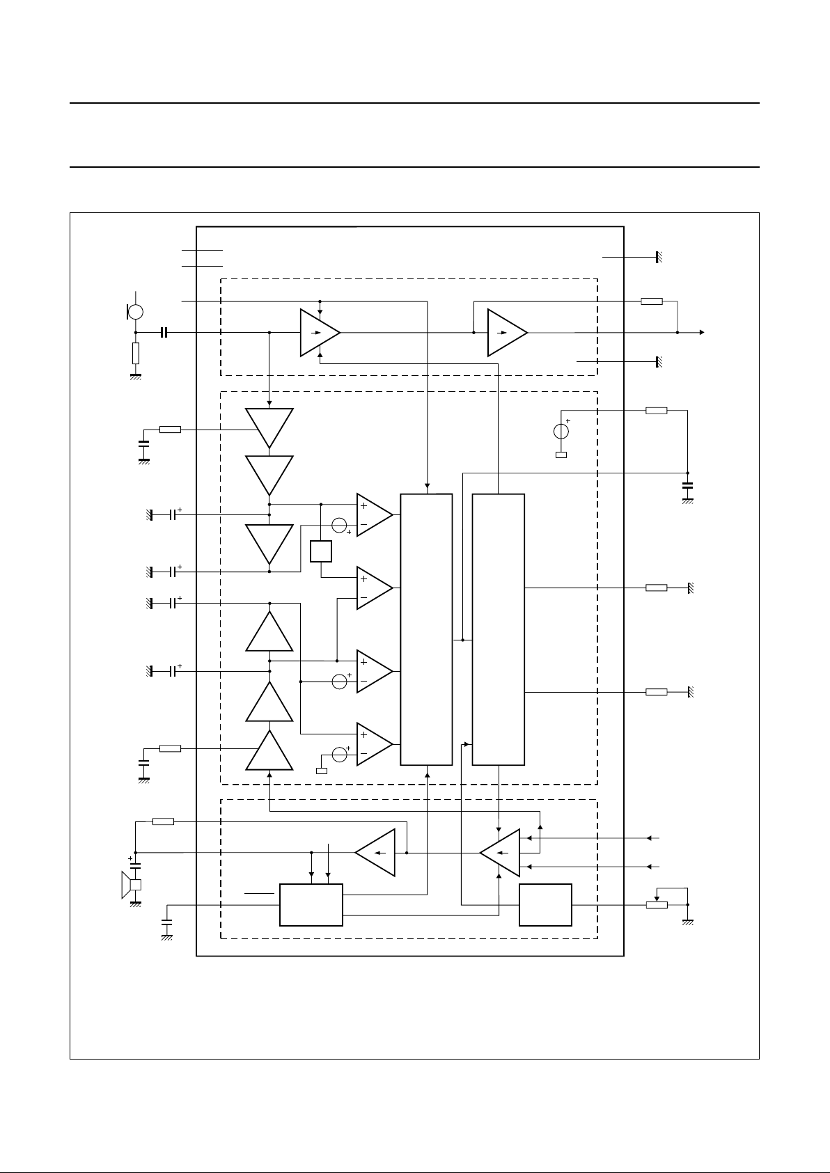
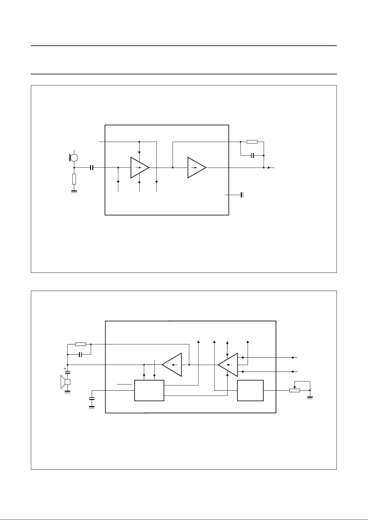
BLOCK DIAGRAM
Fig.1 Block diagram.
handbook, full pagewidth
MGE436
LOG
BUFF
BUFF
LOG
BUFF
BUFF
LOGIC
V I
I V
VOICE
SWITCH
DYNAMIC
LIMITER
VOLUME
CONTROL
I V
V I
DLC/MUTER
LSP
GAR
RSEN
RENV
RNOI
TNOI
TENV
TSEN
MIC
MUTET
VOL
RIN2
RIN1
SWR
STAB
SWT
IDT
MICGND
MOUT
GAT
GND
V
BB
PD
(1)
10
(7)
(13)
19
(15)
22
(18)
28
(24)
27
(23)
26
(22)
23
(19)
24
(20)
25
(21)
5
(4)
6
(5)
1
(1)
8
(6)
21
(17)
20
(16)
18
(14)
16
(12)
14
(11)
13
(10)
12
(9)
2
(2)
2
3
(3)
11
(8)
13 mV
ATTENUATOR
13 mV
V
dt
V
ref
V
BB
V
BB
C
MIC
R
MIC
R
TSEN
C
TSEN
C
TENV
C
TNOI
C
RNOI
C
RENV
R
RSEN
C
RSEN
R
GAR
C
LSP
C
DLC
R
GAT
to TEA106x
R
IDT
C
SWT
R
STAB
R
SWR
from
TEA106x
R
VOL
LOUDSPEAKER CHANNEL
DUPLEX
CONTROLLER
MICROPHONE CHANNEL
TEA1094
TEA1094A
The pin numbers given in parenthesis are for the TEA1094A.
(1) TEA1094A only.
Page 5

1996 Jul 15 5
Philips Semiconductors Product specification
Hands free IC TEA1094; TEA1094A
PINNING
SYMBOL
PINS
DESCRIPTION
TEA1094 TEA1094A
DLC/
MUTER 1 1 dynamic limiter timing adjustment; receiver channel mute input
RIN1 2 2 receiver amplifier input 1
RIN2 3 3 receiver amplifier input 2
n.c. 4 − not connected
GAR 5 4 receiver gain adjustment
LSP 6 5 loudspeaker amplifier output
n.c. 7 − not connected
GND 8 6 ground reference
n.c. 9 − not connected
V
BB
10 7 supply voltage
VOL 11 8 receiver volume adjustment
SWR 12 9 switching range adjustment
STAB 13 10 reference current adjustment
SWT 14 11 switch-over timing adjustment
n.c. 15 − not connected
IDT 16 12 idle mode timing adjustment
PD − 13 power-down input
n.c. 17 − not connected
MICGND 18 14 ground reference for the microphone amplifier
MUTET 19 15 transmit channel mute input
MOUT 20 16 microphone amplifier output
GAT 21 17 microphone gain adjustment
MIC 22 18 microphone input
RNOI 23 19 receive noise envelope timing adjustment
RENV 24 20 receive signal envelope timing adjustment
RSEN 25 21 receive signal envelope sensitivity adjustment
TNOI 26 22 transmit noise envelope timing adjustment
TENV 27 23 transmit signal envelope timing adjustment
TSEN 28 24 transmit signal envelope sensitivity adjustment
Page 6
1996 Jul 15 6
Philips Semiconductors Product specification
Hands free IC TEA1094; TEA1094A
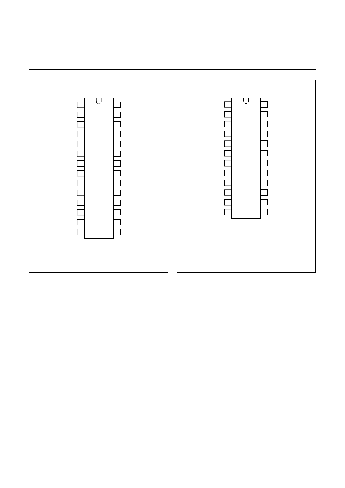
Fig.2 Pin configuration (TEA1094).
handbook, halfpage
DLC/MUTER
RIN1
RIN2
n.c.
GAR
LSP
n.c.
GND
n.c.
V
BB
VOL
SWR
STAB
SWT
TSEN
TENV
TNOI
RSEN
RNOI
MIC
RENV
GAT
MOUT
MUTET
MICGND
n.c.
IDT
n.c.
1
2
3
4
5
6
7
8
9
10
11
12
13
28
27
26
25
24
23
22
21
20
19
18
17
16
1514
TEA1094
MGE434
Fig.3 Pin configuration (TEA1094A).
handbook, halfpage
DLC/MUTER
RIN1
RIN2
GAR
LSP
GND
V
BB
VOL
SWR
STAB
SWT
IDT
TSEN
TENV
TNOI
RSEN
RNOI
MIC
RENV
GAT
MOUT
MUTET
MICGND
PD
1
2
3
4
5
6
7
8
9
10
11
12
24
23
22
21
20
19
18
17
16
15
14
13
TEA1094A
MGE435
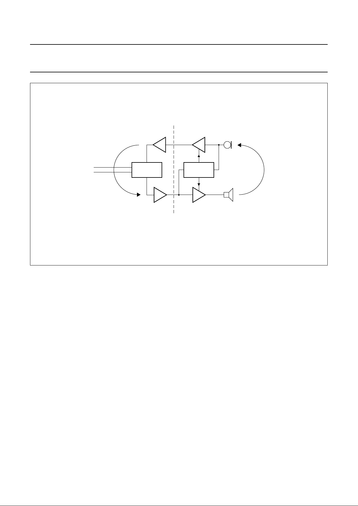
FUNCTIONAL DESCRIPTION
General
The values given in the functional description are typical
values unless otherwise specified.
A principle diagram of the TEA106X is shown on the left
side of Fig.4. The TEA106X is a transmission circuit of the
TEA1060 family intended for hand-set operation.
It incorporates a receiving amplifier for the earpiece, a
transmit amplifier for the microphone and a hybrid.
For more details on the TEA1060 family, please refer to
“data Handbook IC03”
. The right side of Fig.4 shows a
principle diagram of the TEA1094 and TEA1094A,
hands-free add-on circuits with a microphone amplifier, a
loudspeaker amplifier and a duplex controller.
As can be seen from Fig.4, a loop is formed via the
sidetone network in the transmission circuit and the
acoustic coupling between loudspeaker and microphone
of the hands-free circuit. When this loop gain is greater
than 1, howling is introduced. In a full duplex application,
this would be the case.
The loop-gain has to be much lower than 1 and therefore
has to be decreased to avoid howling. This is achieved by
the duplex controller. The duplex controller of the
TEA1094 and TEA1094A detects which channel has the
‘largest’ signal and then controls the gain of the
microphone amplifier and the loudspeaker amplifier so that
the sum of the gains remains constant.
As a result, the circuit can be in three stable modes:
1. Transmit mode (Tx mode).
The gain of the microphone amplifier is at its maximum
and the gain of the loudspeaker amplifier is at its
minimum.
2. Receive mode (Rx mode).
The gain of the loudspeaker amplifier is at its
maximum and the gain of the microphone amplifier is
at its minimum.
3. Idle mode.
The gain of the amplifiers is halfway between their
maximum and minimum value.
The difference between the maximum gain and minimum
gain is called the switching range.
Page 7
1996 Jul 15 7
Philips Semiconductors Product specification
Hands free IC TEA1094; TEA1094A
Fig.4 Hands-free telephone set principles.
handbook, full pagewidth
MGE438
DUPLEX
CONTROL
HYBRID
telephone
line
sidetone
acoustic
coupling
TEA106x
TEA1094
TEA1094A
Supply: pins VBB, GND and PD
The TEA1094 and TEA1094A must be supplied with an
external stabilized voltage source between pins V
BB
and
GND. In the idle mode, without any signal, the internal
supply current is 3.1 mA at VBB=5V.
To reduce the current consumption during pulse dialling or
register recall (flash), the TEA1094A is provided with a
power-down (PD) input. When the voltage on PD is HIGH
the current consumption from VBB is 180 µA.
Microphone channel: pins MIC, GAT, MOUT, MICGND
and MUTET (see Fig.5)
The TEA1094 and TEA1094A have an asymmetrical
microphone input MIC with an input resistance of 20 kΩ.
The gain of the input stage varies according to the mode
of the TEA1094 and TEA1094A. In the transmit mode, the
gain is at its maximum; in the receive mode, it is at its
minimum and in the idle mode, it is halfway between
maximum and minimum.
Switch-over from one mode to the other is smooth and
click-free. The output capability at pin MOUT is
20 µA (RMS).
In the transmit mode, the overall gain of the microphone
amplifier (from pins MIC to MOUT) can be adjusted from
0 dB up to 31 dB to suit specific application requirements.
The gain is proportional to the value of R
GAT
and equals
15.5 dB with R
GAT
= 30.1 kΩ.
A capacitor must be connected in parallel with R
GAT
to
ensure stability of the microphone amplifier. Together with
R
GAT
, it also provides a first-order low-pass filter.
By applying a HIGH level on pin MUTET, the microphone
amplifier is muted and the TEA1094 and TEA1094A are
automatically forced into the receive mode.
Page 8
1996 Jul 15 8
Philips Semiconductors Product specification
Hands free IC TEA1094; TEA1094A
Fig.5 Microphone channel.
handbook, full pagewidth
MGD343
V I I V
C
MIC
V
BB
R
MIC
MUTET
MIC
from
voice
switch
to
envelope
detector
MICGND
MOUT
GAT 21
(17)
19
(15)
22
(18)
20
(16)
18
(14)
to TEA106X
R
GAT
C
GAT
to
logic
The pin numbers given in parenthesis refer to the TEA1094A.
Loudspeaker channel
Fig.6 Loudspeaker channel.
handbook, full pagewidth
MGE437
DYNAMIC
LIMITER
VOLUME
CONTROL
I V
V I
DLC/MUTER
LSP
GAR
VOL
RIN2
RIN1
5
(4)
6
(5)
1
(1)
2
2
(2)
3
(3)
11
(8)
V
BB
R
GAR
C
GAR
C
LSP
C
DLC
from
TEA106x
R
VOL
to
logic
to/from
voice switch
to
envelope
detector
The pin numbers given in parenthesis refer to the TEA1094A.
Page 9

1996 Jul 15 9
Philips Semiconductors Product specification
Hands free IC TEA1094; TEA1094A
LOUDSPEAKER AMPLIFIER: PINS RIN1, RIN2, GAR AND LSP
The TEA1094 and TEA1094A have symmetrical inputs for
the loudspeaker amplifier with an input resistance of 40 kΩ
between RIN1 and RIN2 (2 × 20 kΩ). The input stage can
accommodate signals up to 390 mV (RMS) at room
temperature for 2% of total harmonic distortion (THD).
The gain of the input stage varies according to the mode
of the TEA1094 and TEA1094A. In the receive mode, the
gain is at its maximum; in the transmit mode, it is at its
minimum and in the idle mode, it is halfway between
maximum and minimum. Switch-over from one mode to
the other is smooth and click-free. The rail-to-rail output
stage is designed to power a loudspeaker connected as a
single-ended load (between LSP and GND).
In the receive mode, the overall gain of the loudspeaker
amplifier can be adjusted from 0 dB up to 33 dB to suit
specific application requirements. The gain from
RIN1 and RIN2 to LSP is proportional to the value of R
GAR
and equals 18.5 dB with R
GAR
= 66.5 kΩ. A capacitor
connected in parallel with R
GAR
can be used to provide a
first-order low-pass filter.
V
OLUME CONTROL: PIN VOL
The loudspeaker amplifier gain can be adjusted with the
potentiometer R
VOL
. A linear potentiometer can be used to
obtain logarithmic control of the gain at the loudspeaker
amplifier. Each 950 Ω increase of R
VOL
results in a gain
loss of 3 dB. The maximum gain reduction with the volume
control is internally limited to the switching range.
D
YNAMIC LIMITER: PIN DLC/MUTER
The dynamic limiter of the TEA1094 and TEA1094A
prevents clipping of the loudspeaker output stage and
protects the operation of the circuit when the supply
voltage at VBB falls below 2.9 V.
Hard clipping of the loudspeaker output stage is prevented
by rapidly reducing the gain when the output stage starts
to saturate. The time in which gain reduction is effected
(clipping attack time) is approximately a few milliseconds.
The circuit stays in the reduced gain mode until the peaks
of the loudspeaker signals no longer cause saturation.
The gain of the loudspeaker amplifier then returns to its
normal value within the clipping release time (typically
250 ms). Both attack and release times are proportional to
the value of the capacitor C
DLC
. The total harmonic
distortion of the loudspeaker output stage, in reduced gain
mode, stays below 5% up to 10 dB (minimum) of input
voltage overdrive [providing V
RIN
is below 390 mV (RMS)].
When the supply voltage drops below an internal threshold
voltage of 2.9 V, the gain of the loudspeaker amplifier is
rapidly reduced (approximately 1 ms). When the supply
voltage exceeds 2.9 V, the gain of the loudspeaker
amplifier is increased again.
By forcing a level lower than 0.2 V on pin DLC/
MUTER, the
loudspeaker amplifier is muted and the TEA1094
(TEA1094A) is automatically forced into the transmit
mode.
Duplex controller
S
IGNAL AND NOISE ENVELOPE DETECTORS: PINS TSEN,
TENV, TNOI, RSEN, RENV
AND RNOI
The signal envelopes are used to monitor the signal level
strength in both channels. The noise envelopes are used
to monitor background noise in both channels. The signal
and noise envelopes provide inputs for the decision logic.
The signal and noise envelope detectors are shown in
Fig.7.
For the transmit channel, the input signal at MIC is 40 dB
amplified to TSEN. For the receive channel, the differential
signal between RIN1 and RIN2 is 0 dB amplified to RSEN.
The signals from TSEN and RSEN are logarithmically
compressed and buffered to TENV and RENV
respectively. The sensitivity of the envelope detectors is
set with R
TSEN
and R
RSEN
. The capacitors connected in
series with the two resistors block any DC component and
form a first-order high-pass filter. In the basic application,
see Fig.13, it is assumed that V
MIC
= 1 mV (RMS) and
V
RIN
= 100 mV (RMS) nominal and both R
TSEN
and R
RSEN
have a value of 10 kΩ. With the value of C
TSEN
and C
RSEN
at 100 nF, the cut-off frequency is at 160 Hz.
The buffer amplifiers leading the compressed signals to
TENV and RENV have a maximum source current of
120 µA and a maximum sink current of 1 µA. Together with
the capacitor C
TENV
and C
RENV
, the timing of the signal
envelope monitors can be set. In the basic application, the
value of both capacitors is 470 nF. Because of the
logarithmic compression, each 6 dB signal increase
means 18 mV increase of the voltage on the envelopes
TENV or RENV at room temperature. Thus, timings can be
expressed in dB/ms. At room temperature, the 120 µA
sourced current corresponds to a maximum rise-slope of
the signal envelope of 85 dB/ms. This is sufficient to track
normal speech signals. The 1 µA current sunk by TENV or
RENV corresponds to a maximum fall-slope of 0.7 dB/ms.
This is sufficient for a smooth envelope and also eliminates
the effect of echoes on switching behaviour.
Page 10

1996 Jul 15 10
Philips Semiconductors Product specification
Hands free IC TEA1094; TEA1094A
To determine the noise level, the signals on TENV and
RENV are buffered to TNOI and RNOI. These buffers have
a maximum source current of 1 µA and a maximum sink
current of 120 µA. Together with the capacitors C
TNOI
and
C
RNOI
, the timing can be set. In the basic application of
Fig.13 the value of both capacitors is 4.7 µF. At room
temperature, the 1 µA sourced current corresponds to a
maximum rise-slope of the noise envelope of
approximately 0.07 dB/ms.
This is small enough to track background noise and not to
be influenced by speech bursts. The 120 µA current that is
sunk corresponds to a maximum fall-slope of
approximately 8.5 dB/ms. However, during the decrease
of the signal envelope, the noise envelope tracks the
signal envelope so it will never fall faster than
approximately 0.7 dB/ms. The behaviour of the signal
envelope and noise envelope monitors is illustrated in
Fig.8.
Fig.7 Signal and noise envelope detectors.
handbook, full pagewidth
MGD223
LOG
28
(24)
27
(23)
26
(22)
25
(21)
24
(20)
23
(19)
LOG
from
microphone
amplifier
from
loudspeaker
amplifier
DUPLEX CONTROLLER
TSEN
R
TSEN
C
TSEN
C
TENV
C
TNOI
R
RSEN
C
RSEN
C
RENV
C
RNOI
TENV TNOI RSEN RENV RNOI
to logicto logic
The pin numbers given in parenthesis refer to the TEA1094A.
handbook, full pagewidth
MBG354
INPUT SIGNAL
SIGNAL ENVELOPE
NOISE ENVELOPE
4 mV (RMS)
1 mV (RMS)
A
C
C
36 mV
36 mV
B
B
B
A
B
time
A: 85 dB/ms
B: 0.7 dB/ms
B: 0.7 dB/ms
C: 0.07 dB/ms
Fig.8 Signal and noise envelope waveforms.
Page 11

1996 Jul 15 11
Philips Semiconductors Product specification
Hands free IC TEA1094; TEA1094A
DECISION LOGIC: PINS IDT AND SWT
Fig.9 Decision logic.
The pin numbers given in parenthesis refer to the TEA1094A.
(1) When MUTET = HIGH, +10 µA is forced.
When DLC/MUTER < 0.2 V, −10 µA is forced.
handbook, full pagewidth
MGD224
13 mV
13 mV
TENV
TNOI
RENV
MUTET
from dynamic
limiter
RNOI
V
dt
XX11− 10 µA
+ 10 µA
+ 10 µA
X10X
1X0X
XX10 0
000X 0
V
ref
R
IDT
C
SWT
SWT
16
(12)
14
(11)
27
(23)
26
(22)
24
(20)
23
(19)
19
(15)
IDT
DUPLEX CONTROLLER
LOGIC
(1)
ATTENUATOR
The TEA1094 and TEA1094A select their modes of
operation (transmit, receive or idle mode) by comparing
the signal and the noise envelopes of both channels. This
is executed by the decision logic. The resulting voltage on
pin SWT is the input for the voice-switch.
To facilitate the distinction between signal and noise, the
signal is considered as speech when its envelope is more
than 4.3 dB above the noise envelope. At room
temperature, this is equal to a voltage difference
V
ENV
− V
NOI
= 13 mV. This so called speech/noise
threshold is implemented in both channels.
The signal on MIC contains both speech and the signal
coming from the loudspeaker (acoustic coupling). When
receiving, the contribution from the loudspeaker overrules
the speech.
As a result, the signal envelope on TENV is formed mainly
by the loudspeaker signal. To correct this, an attenuator is
connected between TENV and the TENV/RENV
comparator. Its attenuation equals that applied to the
microphone amplifier.
When a dial tone is present on the line, without monitoring,
the tone would be recognized as noise because it is a
signal with a constant amplitude. This would cause the
TEA1094 (TEA1094A) to go into the idle mode and the
user of the set would hear the dial tone fade away. To
prevent this, a dial tone detector is incorporated which, in
standard applications, does not consider input signals
between RIN1 and RIN2 as noise when they have a level
greater than 127 mV (RMS). This level is proportional to
R
RSEN
.
Page 12

1996 Jul 15 12
Philips Semiconductors Product specification
Hands free IC TEA1094; TEA1094A
As can be seen from Fig.9, the output of the decision logic
is a current source. The logic table gives the relationship
between the inputs and the value of the current source.
It can charge or discharge the capacitor C
SWT
with a
current of 10 µA (switch-over). If the current is zero, the
voltage on SWT becomes equal to the voltage on IDT via
the high-ohmic resistor R
IDT
(idling). The resulting voltage
difference between SWT and IDT determines the mode of
the TEA1094 (TEA1094A) and can vary between
−400 and +400 mV (see Table 1).
Table 1 Modes of TEA1094; TEA1094A
The switch-over timing can be set with C
SWT
, the idle mode
timing with C
SWT
and R
IDT
. In the basic application given in
Fig.13, C
SWT
is 220 nF and R
IDT
is 2.2 MΩ. This enables a
switch-over time from transmit to receive mode or
vice-versa of approximately 13 ms (580 mV swing on
SWT). The switch-over time from idle mode to transmit
mode or receive mode is approximately 4 ms (180 mV
swing on SWT).
The switch-over time, from receive mode or transmit mode
to idle mode, is equal to 4 × R
IDTCSWT
and is
approximately 2 seconds (idle mode time).
The inputs MUTET and DLC/MUTER overrule the decision
logic. When MUTET goes HIGH, the capacitor C
SWT
is
charged with 10 µA thus resulting in the receive mode.
When the voltage on pin DLC/MUTER goes lower than
0.2 V, the capacitor C
SWT
is discharged with 10 µA thus
resulting in the transmit mode.
V
OICE-SWITCH: PINS STAB AND SWR
A diagram of the voice-switch is illustrated in Fig.10. With
the voltage on SWT, the TEA1094 (TEA1094A)
voice-switch regulates the gains of the transmit and the
receive channel so that the sum of both is kept constant.
In the transmit mode, the gain of the microphone amplifier
is at its maximum and the gain of the loudspeaker amplifier
is at its minimum. In the receive mode, the opposite
applies. In the idle mode, both microphone and
loudspeaker amplifier gains are halfway.
V
SWT
− V
IDT
(mV) MODE
<−180 transmit mode
0 idle mode
>180 receive mode
The difference between maximum and minimum is the so
called switching range. This range is determined by the
ratio of R
SWR
and R
STAB
and is adjustable between
0 and 52 dB. R
STAB
should be 3.65 kΩ and sets an
internally used reference current. In the basic application
diagram given in Fig.13, R
SWR
is 365 kΩ which results in a
switching range of 40 dB. The switch-over behaviour is
illustrated in Fig.11.
In the receive mode, the gain of the loudspeaker amplifier
can be reduced using the volume control. Since the
voice-switch keeps the sum of the gains constant, the gain
of the microphone amplifier is increased at the same time
(see dashed curves in Fig.11). In the transmit mode,
however, the volume control has no influence on the gain
of the microphone amplifier or the gain of the loudspeaker
amplifier. Consequently, the switching range is reduced
when the volume is reduced. At maximum reduction of
volume, the switching range becomes 0 dB.
Fig.10 Voice switch.
The pin numbers given in parenthesis refer to the TEA1094A.
(1) C = constant.
G
vtx
+ G
vrx =
C
(1)
VOICE SWITCH
R
STAB
R
SWR
STAB
13
(10)
12
(9)
SWR
to
microphone
amplifier
from
SWT
from
volume
control
to
loudspeaker
amplifier
DUPLEX CONTROLLER
MGD225
Page 13

1996 Jul 15 13
Philips Semiconductors Product specification
Hands free IC TEA1094; TEA1094A
LIMITING VALUES
In accordance with the Absolute Maximum Rating System (IEC 134).
SYMBOL PARAMETER CONDITIONS MIN. MAX. UNIT
V
n(max)
maximum voltage on all pins; except pins
VBB, RIN1 and RIN2
V
GND
− 0.4 VBB+ 0.4 V
V
RIN(max)
maximum voltage on pins RIN1 and RIN2 V
GND
− 1.2 VBB+ 0.4 V
V
BB(max)
maximum voltage on pin V
BB
V
GND
− 0.4 12.0 V
P
tot
total power dissipation T
amb
=75°C
TEA1094 − 1000 mW
TEA1094A − 910 mW
TEA1094T − 625 mW
TEA1094AT − 590 mW
TEA1094AM − 438 mW
T
stg
IC storage temperature −40 +125 °C
T
amb
operating ambient temperature −25 +75 °C
Fig.11 Switch-over behaviour.
handbook, halfpage
−400 −200 0 +400+200
G
vtx,
G
vrx
V
SWT −
V
IDT
(mV)
G
vtx
R
VOL
(Ω)
5700
3800
idle
mode
1900
0
0
1900
3800
5700
(10 dB/div)
Tx mode Rx mode
G
vrx
MBG351
Page 14

1996 Jul 15 14
Philips Semiconductors Product specification
Hands free IC TEA1094; TEA1094A
THERMAL CHARACTERISTICS
CHARACTERISTICS
V
BB
=5V; V
GND
= 0 V; f = 1 kHz; T
amb
=25°C; MUTET = LOW; PD = LOW (TEA1094A only); RL=50Ω; R
VOL
=0Ω;
measured in test circuit of Fig.12; unless otherwise specified.
SYMBOL PARAMETER VALUE UNIT
R
th j-a
thermal resistance from junction to ambient in free air
TEA1094 45 K/W
TEA1094A 50 K/W
TEA1094T 70 K/W
TEA1094AT 75 K/W
TEA1094AM 104 K/W
SYMBOL PARAMETER CONDITIONS MIN. TYP. MAX. UNIT
Supply (V
BB
, GND and PD)
V
BB
supply voltage 3.3 − 12.0 V
I
BB
current consumption from pin V
BB
− 3.1 4.4 mA
POWER-DOWN INPUT PD (TEA1094A ONLY)
V
IL
LOW level input voltage V
GND
− 0.4 − 0.3 V
V
IH
HIGH level input voltage 1.5 − VBB+ 0.4 V
I
PD
input current PD = HIGH − 2.5 5 µA
I
BB(PD)
current consumption from pin V
BB
in power-down condition
PD = HIGH − 180 240 µA
Microphone channel (MIC, GAT, MOUT, MUTET and MICGND)
M
ICROPHONE AMPLIFIER
|Zi| input impedance between
pins MIC and MICGND
17 20 23 kΩ
G
vtx
voltage gain from pin MIC to
MOUT in transmit mode
V
MIC
= 1 mV (RMS) 13 15.5 18 dB
∆G
vtxr
voltage gain adjustment with R
GAT
−15.5 − +15.5 dB
∆G
vtxT
voltage gain variation with
temperature referenced to 25 °C
V
MIC
= 1 mV (RMS);
T
amb
= −25 to +75 °C
−±0.3 − dB
∆G
vtxf
voltage gain variation with
frequency referenced to 1 kHz
V
MIC
= 1 mV (RMS);
f = 300 to 3400 Hz
−±0.3 − dB
V
notx
noise output voltage at pin MOUT pin MIC connected to
MICGND through 200 Ω in
series with 10 µF;
psophometrically weighted
(P53 curve)
−−100 − dBmp
Page 15

1996 Jul 15 15
Philips Semiconductors Product specification
Hands free IC TEA1094; TEA1094A
TRANSMIT MUTE INPUT MUTET
V
IL
LOW level input voltage V
GND
− 0.4 − 0.3 V
V
IH
HIGH level input voltage 1.5 − VBB+ 0.4 V
I
MUTET
input current MUTET = HIGH − 2.5 5 µA
∆G
vtxm
voltage gain reduction with
MUTET active
MUTET = HIGH − 80 − dB
Loudspeaker channel (RIN1, RIN2, GAR, LSP and DLC/
MUTER)
LOUDSPEAKER AMPLIFIER
|Zi| input impedance between pins RIN1 or RIN2
and GND
17 20 23 kΩ
between pins RIN1 and
RIN2
34 40 46 kΩ
G
vrx
voltage gain in receive mode;
between RIN1 and RIN2 to LSP
V
RIN
= 20 mV (RMS) 16 18.5 21 dB
∆G
vrxr
voltage gain adjustment with R
GAR
−18.5 − +14.5 dB
∆G
vrxT
voltage gain variation with
temperature referenced to 25 °C
V
RIN
= 20 mV (RMS);
T
amb
= −25 to +75 °C
−±0.3 − dB
∆G
vrxf
voltage gain variation with
frequency referenced to 1 kHz
V
RIN
= 20 mV (RMS);
f = 300 to 3400 Hz
−±0.3 − dB
V
RIN(rms)
maximum input voltage between
RIN1 and RIN2 (RMS value)
R
GAR
= 11.8 kΩ; for 2%
THD in input stage
− 390 − mV
V
norx(rms)
noise output voltage at pin LSP
(RMS value)
inputs RIN1 and RIN2
short-circuited through
200 Ω in series with 10 µF;
psophometrically weighted
(P53 curve)
− 80 −µV
CMRR common mode rejection ratio − 50 − dB
∆G
vrxv
voltage gain variation related to
∆R
VOL
= 950 Ω
when total attenuation does
not exceed the switching
range
− 3 − dB
OUTPUT CAPABILITY
V
OSE(p-p)
output voltage
(peak-to-peak value)
V
RIN
= 300 mV (RMS);
note 1
3.5 4.5 − V
V
RIN
= 150 mV (RMS);
R
GAR
= 374 kΩ; RL=33Ω;
VBB= 9.0 V; note 2
− 7.5 − V
I
OM
maximum output current at LSP
(peak value)
150 500 − mA
SYMBOL PARAMETER CONDITIONS MIN. TYP. MAX. UNIT
Page 16

1996 Jul 15 16
Philips Semiconductors Product specification
Hands free IC TEA1094; TEA1094A
DYNAMIC LIMITER
t
att
attack time when V
RIN
jumps from
20 mV to 20 mV + 10 dB
R
GAR
= 374 kΩ−−5ms
t
rel
release time when V
RIN
jumps
from 20 mV + 10 dB to 20 mV
R
GAR
= 374 kΩ−250 − ms
THD total harmonic distortion at
V
RIN
=20mV+10dB
R
GAR
= 374 kΩ; t > t
att
− 0.9 5 %
V
BB(th)
VBB limiter threshold − 2.9 − V
t
att
attack time when VBB jumps below
V
BB(th)
− 1 − ms
MUTE RECEIVE
V
DLC(th)
threshold voltage required on pin
DLC/MUTER to obtain mute
receive condition
V
GND
− 0.4 − 0.2 V
I
DLC(th)
threshold current sourced by
pin DLC/MUTER in mute receive
condition
V
DLC
= 0.2 V − 100 −µA
∆G
vrxm
voltage gain reduction in mute
receive condition
V
DLC
< 0.2 V − 80 − dB
Envelope and noise detectors (TSEN, TENV, RSEN, RENV, RNOI and TNOI)
P
REAMPLIFIERS
G
v(TSEN)
voltage gain from MIC to TSEN 37.5 40 42.5 dB
G
v(RSEN)
voltage gain between RIN1 and
RIN2 to RSEN
−2.5 0 +2.5 dB
LOGARITHMIC COMPRESSOR AND SENSITIVITY ADJUSTMENT
∆V
det(TSEN)
sensitivity detection on pin TSEN;
voltage change on pin TENV
when doubling the current from
TSEN
I
TSEN
= 0.8 to 160 µA − 18 − mV
∆V
det(RSEN)
sensitivity detection on
pin RSEN; voltage change on
pin RENV when doubling the
current from RSEN
I
RSEN
= 0.8 to 160 µA − 18 − mV
SIGNAL ENVELOPE DETECTORS
I
source(ENV)
maximum current sourced from
pin TENV or RENV
− 120 −µA
I
sink(ENV)
maximum current sunk by
pin TENV or RENV
0.75 1 1.25 µA
∆V
ENV
voltage difference between
pins RENV and TENV
when 10 µA is sourced
from both RSEN and
TSEN; envelope detectors
tracking; note 3
−±3−mV
SYMBOL PARAMETER CONDITIONS MIN. TYP. MAX. UNIT
Page 17

1996 Jul 15 17
Philips Semiconductors Product specification
Hands free IC TEA1094; TEA1094A
Notes
1. Corresponds to 50 mW output power.
2. Corresponds to 200 mW output power.
3. Corresponds to ±1 dB tracking.
4. Corresponds to 4.3 dB noise/speech recognition level.
N
OISE ENVELOPE DETECTORS
I
source(NOI)
maximum current sourced from
pins TNOI or RNOI
0.75 1 1.25 µA
I
sink(NOI)
maximum current sunk by
pins TNOI or RNOI
− 120 −µA
∆V
NOI
voltage difference between
pins RNOI and TNOI
when 5 µA is sourced from
both RSEN and TSEN;
noise detectors tracking;
note 3
−±3−mV
DIAL TONE DETECTOR
V
RINDT(rms)
threshold level at pins RIN1 and
RIN2 (RMS value)
− 127 − mV
Decision logic (IDT and SWT)
S
IGNAL RECOGNITION
∆V
Srx(th)
threshold voltage between
pins RENV and RNOI to
switch-over from receive to idle
mode
V
RIN
< V
RINDT
; note 4 − 13 − mV
∆V
Stx(th)
threshold voltage between
pins TENV and TNOI to
switch-over from transmit to idle
mode
note 4 − 13 − mV
SWITCH-OVER
I
source(SWT)
current sourced from pin SWT
when switching to receive mode
7.5 10 12.5 µA
I
sink(SWT)
current sunk by pin SWT when
switching to transmit mode
7.5 10 12.5 µA
I
idle(SWT)
current sourced from pin SWT in
idle mode
− 0 −µA
Voice switch (STAB and SWR)
SWRA switching range − 40 − dB
∆SWRA switching range adjustment with R
SWR
referenced to
365 kΩ
−40 − +12 dB
|∆G
v
| voltage gain variation from
transmit mode to idle mode on
both channels
− 20 − dB
G
tr
gain tracking (G
vtx+Gvrx
) during
switching, referenced to idle mode
−±0.5 − dB
SYMBOL P ARAMETER CONDITIONS MIN. TYP. MAX. UNIT
Page 18

1996 Jul 15 18
Philips Semiconductors Product specification
Hands free IC TEA1094; TEA1094A
Fig.12 Test circuit.
handbook, full pagewidth
MGE439
VOLDLC/MUTERTNOITENVTSENRNOIRENVRSEN
GND
MICGND
RIN2
RIN1
GAT
MOUT
PD
(1)
MUTET IDT SWT STAB SWR
V
BB
MIC
GAR
LSP
20
(16)
21
(17)
2
(2)
3
(3)
18
(14)
8
(6)
25
(21)
24
(20)
28
(24)
27
(23)
26
(22)
23
(19)
1
(1)
11
(8)
6
(5)
5
(4)
22
(18)
10
(7)
12
(9)
13
(10)
14
(11)
16
(12)
19
(15)(13)
R
SWR
365
kΩ
R
STAB
3.65
kΩ
C
SWT
220
nF
R
IDT
2.2
MΩ
30.1
kΩ
R
GAT
C
GAT
C
RIN2
C
RIN1
220 nF
220 nF
R
RSEN
C
RSENCRENVCRNOI
C
TNOI
C
TSENCTENV
C
DLC
4.7
µF
4.7
µF
100
nF
470
nF
470
nF
R
TSEN
10 kΩ
R
VOL
C
GAR
R
GAR
66.5
kΩ
C
MIC
220 nF
V
MIC
V
VBB
C
VBB
10 µF
TEA1094
TEA1094A
C
LSP
47 µF
R
L
50 Ω
V
RIN1
10 kΩ
100
nF
470
nF
The pin numbers given in parenthesis refer to the TEA1094A.
(1) TEA1094A only.
Page 19

1996 Jul 15 19
Philips Semiconductors Product specification
Hands free IC TEA1094; TEA1094A
APPLICATION INFORMATION
bo
ok, full pagewidth
MGE440
C7
100 nF
C8
100 nF
20 Ω
R9
C1
100
µF
620 Ω
R1
V
CC
LN
MIC−
MIC+
QR+
V
EE
SLPE
line
TEA106x
VOLDLC/MUTERTNOITENVTSENRNOIRENVRSEN
GND
MICGND
RIN2
RIN1
GAT
MOUT
PD
(1)
MUTET IDT SWT STAB SWR
V
BB
MIC
GAR
LSP
20
(16)
21
(17)
2
(2)
3
(3)
18
(14)
8
(6)
25
(21)24(20)
28
(24)27(23)26(22)
23
(19)
1
(1)11(8)
6
(5)
5
(4)
22
(18)
10
(7)
12
(9)
13
(10)
14
(11)
16
(12)
19
(15)
(13)
R
SWR
365
kΩ
R
STAB
3.65
kΩ
C
SWT
220
nF
R
IDT
2.2
MΩ
30.1
kΩ
R
GAT
C
GAT
C
RIN1
100 nF
R
RSEN
C
RSENCRENVCRNOI
C
TNOI
C
TSENCTENV
C
DLC
4.7
µF
4.7
µF
100
nF
470
nF
470
nF
R
TSEN
10 kΩ
R
VOL
C
GAR
R
GAR
66.5
kΩ
C
MIC
100 nF
V
VBB
C
VBB
10 µF
TEA1094
TEA1094A
C
LSP
47 µF
50 Ω
R
LSP
10 kΩ
100
nF
470
nF
R
MIC
2.2 kΩ
Fig.13 Basic application diagram.
The pin numbers given in parenthesis refer to the TEA1094A.
(1) TEA1094A only.
Page 20

1996 Jul 15 20
Philips Semiconductors Product specification
Hands free IC TEA1094; TEA1094A
b
ook, full pagewidth
MGE441
MICRO-
CONTROLLER
DP DTMF DTMF
100 nF
100 nF
C7a
C7b
C
VBB
10 µF
V
VBB
R
MIC
2.2 kΩ
C
MIC
100 nF
C8
2.2 kΩ
TEA1094
TEA1094A
MUTET
PD
(1)
V
BB
MIC
C
LSP
50 Ω
LSP
10
(7)
22
(18)
C
RIN1
100 nF
2
(2)
MOUT
RIN1
MICGND
GND
20
(16)
18
(14)
8
(6)
TEA106x
MIC−
MIC+
QR+
LNV
CC
10 µF
S2
20 Ω
R9
tip
ring
620 Ω
R1
1 kΩ
100 µF
S1
SLPE
V
EE
LSP
6
(5)
(13)
19
(15)
from
microcontroller
100 µF
C1
interrupter
Fig.14 Application example.
The pin numbers given in parenthesis refer to the TEA1094A.
(1) TEA1094A only.
Page 21

1996 Jul 15 21
Philips Semiconductors Product specification
Hands free IC TEA1094; TEA1094A
PACKAGE OUTLINES
UNIT
A
max.
1 2
b
1
(1)
(1) (1)
cD E weM
H
L
REFERENCES
OUTLINE
VERSION
EUROPEAN
PROJECTION
ISSUE DATE
IEC JEDEC EIAJ
mm
inches
DIMENSIONS (inch dimensions are derived from the original mm dimensions)
SOT117-1
92-11-17
95-01-14
A
min.
A
max.
b
Z
max.
M
E
e
1
1.7
1.3
0.53
0.38
0.32
0.23
36.0
35.0
14.1
13.7
3.9
3.4
0.252.54 15.24
15.80
15.24
17.15
15.90
1.75.1 0.51 4.0
0.066
0.051
0.020
0.014
0.013
0.009
1.41
1.34
0.56
0.54
0.15
0.13
0.010.10 0.60
0.62
0.60
0.68
0.63
0.0670.20 0.020 0.16
051G05 MO-015AH
M
H
c
(e )
1
M
E
A
L
seating plane
A
1
w M
b
1
e
D
A
2
Z
28
1
15
14
b
E
pin 1 index
0 5 10 mm
scale
Note
1. Plastic or metal protrusions of 0.25 mm maximum per side are not included.
handbook, full pagewidth
DIP28: plastic dual in-line package; 28 leads (600 mil)
SOT117-1
Page 22

1996 Jul 15 22
Philips Semiconductors Product specification
Hands free IC TEA1094; TEA1094A
UNIT
A
max.
1 2
b
1
cD E e M
H
L
REFERENCES
OUTLINE
VERSION
EUROPEAN
PROJECTION
ISSUE DATE
IEC JEDEC EIAJ
mm
inches
DIMENSIONS (inch dimensions are derived from the original mm dimensions)
SOT101-1
92-11-17
95-01-23
A
min.
A
max.
b
w
M
E
e
1
1.7
1.3
0.53
0.38
0.32
0.23
32.0
31.4
14.1
13.7
3.9
3.4
0.252.54 15.24
15.80
15.24
17.15
15.90
2.25.1 0.51 4.0
0.066
0.051
0.021
0.015
0.013
0.009
1.26
1.24
0.56
0.54
0.15
0.13
0.010.10 0.60
0.62
0.60
0.68
0.63
0.0870.20 0.020 0.16
051G02 MO-015AD
M
H
c
(e )
1
M
E
A
L
seating plane
A
1
w M
b
1
e
D
A
2
Z
24
1
13
12
b
E
pin 1 index
0 5 10 mm
scale
Note
1. Plastic or metal protrusions of 0.25 mm maximum per side are not included.
Z
max.
(1)
(1)(1)
DIP24: plastic dual in-line package; 24 leads (600 mil)
SOT101-1
Page 23

1996 Jul 15 23
Philips Semiconductors Product specification
Hands free IC TEA1094; TEA1094A
UNIT
A
max.
A
1
A
2
A
3
b
p
cD
(1)E(1) (1)
eHELLpQ
Z
ywv θ
REFERENCES
OUTLINE
VERSION
EUROPEAN
PROJECTION
ISSUE DATE
IEC JEDEC EIAJ
mm
inches
2.65
0.30
0.10
2.45
2.25
0.49
0.36
0.32
0.23
18.1
17.7
7.6
7.4
1.27
10.65
10.00
1.1
1.0
0.9
0.4
8
0
o
o
0.25 0.1
DIMENSIONS (inch dimensions are derived from the original mm dimensions)
Note
1. Plastic or metal protrusions of 0.15 mm maximum per side are not included.
1.1
0.4
SOT136-1
X
14
28
w M
θ
A
A
1
A
2
b
p
D
H
E
L
p
Q
detail X
E
Z
c
L
v M
A
e
15
1
(A )
3
A
y
0.25
075E06 MS-013AE
pin 1 index
0.10
0.012
0.004
0.096
0.089
0.019
0.014
0.013
0.009
0.71
0.69
0.30
0.29
0.050
1.4
0.055
0.419
0.394
0.043
0.039
0.035
0.016
0.01
0.25
0.01
0.004
0.043
0.016
0.01
0 5 10 mm
scale
SO28: plastic small outline package; 28 leads; body width 7.5 mm
SOT136-1
95-01-24
97-05-22
Page 24

1996 Jul 15 24
Philips Semiconductors Product specification
Hands free IC TEA1094; TEA1094A
UNIT
A
max.
A1A
2
A
3
b
p
cD
(1)E(1) (1)
eHELLpQ
Z
ywv θ
REFERENCES
OUTLINE
VERSION
EUROPEAN
PROJECTION
ISSUE DATE
IEC JEDEC EIAJ
mm
inches
2.65
0.30
0.10
2.45
2.25
0.49
0.36
0.32
0.23
15.6
15.2
7.6
7.4
1.27
10.65
10.00
1.1
1.0
0.9
0.4
8
0
o
o
0.25 0.1
DIMENSIONS (inch dimensions are derived from the original mm dimensions)
Note
1. Plastic or metal protrusions of 0.15 mm maximum per side are not included.
1.1
0.4
SOT137-1
X
12
24
w M
θ
A
A
1
A
2
b
p
D
H
E
L
p
Q
detail X
E
Z
c
L
v M
A
13
(A )
3
A
y
0.25
075E05 MS-013AD
pin 1 index
0.10
0.012
0.004
0.096
0.089
0.019
0.014
0.013
0.009
0.61
0.60
0.30
0.29
0.050
1.4
0.055
0.419
0.394
0.043
0.039
0.035
0.016
0.01
0.25
0.01
0.004
0.043
0.016
0.01
e
1
0 5 10 mm
scale
SO24: plastic small outline package; 24 leads; body width 7.5 mm
SOT137-1
95-01-24
97-05-22
Page 25

1996 Jul 15 25
Philips Semiconductors Product specification
Hands free IC TEA1094; TEA1094A
UNIT A1A
2
A
3
b
p
cD
(1)E(1) (1)
eHELLpQZywv θ
REFERENCES
OUTLINE
VERSION
EUROPEAN
PROJECTION
ISSUE DATE
IEC JEDEC EIAJ
mm
0.21
0.05
1.80
1.65
0.38
0.25
0.20
0.09
8.4
8.0
5.4
5.2
0.65 1.25
7.9
7.6
0.9
0.7
0.8
0.4
8
0
o
o
0.13 0.10.2
DIMENSIONS (mm are the original dimensions)
Note
1. Plastic or metal protrusions of 0.20 mm maximum per side are not included.
1.03
0.63
SOT340-1 MO-150AG
93-09-08
95-02-04
X
w M
θ
A
A
1
A
2
b
p
D
H
E
L
p
Q
detail X
E
Z
e
c
L
v M
A
(A )
3
A
112
24 13
0.25
y
pin 1 index
0 2.5 5 mm
scale
SSOP24: plastic shrink small outline package; 24 leads; body width 5.3 mm
SOT340-1
A
max.
2.0
Page 26

1996 Jul 15 26
Philips Semiconductors Product specification
Hands free IC TEA1094; TEA1094A
SOLDERING
Introduction
There is no soldering method that is ideal for all IC
packages. Wave soldering is often preferred when
through-hole and surface mounted components are mixed
on one printed-circuit board. However, wave soldering is
not always suitable for surface mounted ICs, or for
printed-circuits with high population densities. In these
situations reflow soldering is often used.
This text gives a very brief insight to a complex technology.
A more in-depth account of soldering ICs can be found in
our
“IC Package Databook”
(order code 9398 652 90011).
DIP
SOLDERING BY DIPPING OR BY WA VE
The maximum permissible temperature of the solder is
260 °C; solder at this temperature must not be in contact
with the joint for more than 5 seconds. The total contact
time of successive solder waves must not exceed
5 seconds.
The device may be mounted up to the seating plane, but
the temperature of the plastic body must not exceed the
specified maximum storage temperature (T
stg max
). If the
printed-circuit board has been pre-heated, forced cooling
may be necessary immediately after soldering to keep the
temperature within the permissible limit.
R
EPAIRING SOLDERED JOINTS
Apply a low voltage soldering iron (less than 24 V) to the
lead(s) of the package, below the seating plane or not
more than 2 mm above it. If the temperature of the
soldering iron bit is less than 300 °C it may remain in
contact for up to 10 seconds. If the bit temperature is
between 300 and 400 °C, contact may be up to 5 seconds.
SO and SSOP
REFLOW SOLDERING
Reflow soldering techniques are suitable for all SO and
SSOP packages.
Reflow soldering requires solder paste (a suspension of
fine solder particles, flux and binding agent) to be applied
to the printed-circuit board by screen printing, stencilling or
pressure-syringe dispensing before package placement.
Several techniques exist for reflowing; for example,
thermal conduction by heated belt. Dwell times vary
between 50 and 300 seconds depending on heating
method. Typical reflow temperatures range from
215 to 250 °C.
Preheating is necessary to dry the paste and evaporate
the binding agent. Preheating duration: 45 minutes at
45 °C.
W
AVE SOLDERING
Wave soldering is not recommended for SSOP packages.
This is because of the likelihood of solder bridging due to
closely-spaced leads and the possibility of incomplete
solder penetration in multi-lead devices.
If wave soldering cannot be avoided, the following
conditions must be observed:
• A double-wave (a turbulent wave with high upward
pressure followed by a smooth laminar wave)
soldering technique should be used.
• The longitudinal axis of the package footprint must
be parallel to the solder flow and must incorporate
solder thieves at the downstream end.
Even with these conditions, only consider wave
soldering SSOP packages that have a body width of
4.4 mm, that is SSOP16 (SOT369-1) or
SSOP20 (SOT266-1).
During placement and before soldering, the package must
be fixed with a droplet of adhesive. The adhesive can be
applied by screen printing, pin transfer or syringe
dispensing. The package can be soldered after the
adhesive is cured.
Maximum permissible solder temperature is 260 °C, and
maximum duration of package immersion in solder is
10 seconds, if cooled to less than 150 °C within
6 seconds. Typical dwell time is 4 seconds at 250 °C.
A mildly-activated flux will eliminate the need for removal
of corrosive residues in most applications.
R
EPAIRING SOLDERED JOINTS
Fix the component by first soldering two diagonallyopposite end leads. Use only a low voltage soldering iron
(less than 24 V) applied to the flat part of the lead. Contact
time must be limited to 10 seconds at up to 300 °C. When
using a dedicated tool, all other leads can be soldered in
one operation within 2 to 5 seconds between
270 and 320 °C.
Page 27

1996 Jul 15 27
Philips Semiconductors Product specification
Hands free IC TEA1094; TEA1094A
DEFINITIONS
LIFE SUPPORT APPLICATIONS
These products are not designed for use in life support appliances, devices, or systems where malfunction of these
products can reasonably be expected to result in personal injury. Philips customers using or selling these products for
use in such applications do so at their own risk and agree to fully indemnify Philips for any damages resulting from such
improper use or sale.
Data sheet status
Objective specification This data sheet contains target or goal specifications for product development.
Preliminary specification This data sheet contains preliminary data; supplementary data may be published later.
Product specification This data sheet contains final product specifications.
Limiting values
Limiting values given are in accordance with the Absolute Maximum Rating System (IEC 134). Stress above one or
more of the limiting values may cause permanent damage to the device. These are stress ratings only and operation
of the device at these or at any other conditions above those given in the Characteristics sections of the specification
is not implied. Exposure to limiting values for extended periods may affect device reliability.
Application information
Where application information is given, it is advisory and does not form part of the specification.
Page 28

Internet: http://www.semiconductors.philips.com/ps/
(1) TEA1094_3 June 26, 1996 11:51 am
Philips Semiconductors – a worldwide company
© Philips Electronics N.V. 1996 SCA50
All rights are reserved. Reproduction in whole or in part is prohibited without the prior written consent of the copyright owner.
The information presented in this document does not form part of any quotation or contract, is believed to be accurate and reliable and may be changed
without notice. No liability will be accepted by the publisher for any consequence of its use. Publication thereof does not convey nor imply any license
under patent- or other industrial or intellectual property rights.
Netherlands: Postbus 90050, 5600 PB EINDHOVEN, Bldg. VB,
Tel. +31 40 27 83749, Fax. +31 40 27 88399
New Zealand: 2 Wagener Place, C.P.O. Box 1041, AUCKLAND,
Tel. +64 9 849 4160, Fax. +64 9 849 7811
Norway: Box 1, Manglerud 0612, OSLO,
Tel. +47 22 74 8000, Fax. +47 22 74 8341
Philippines: Philips Semiconductors Philippines Inc.,
106 Valero St. Salcedo Village, P.O. Box 2108 MCC, MAKATI,
Metro MANILA, Tel. +63 2 816 6380, Fax. +63 2 817 3474
Poland: Ul. Lukiska 10, PL 04-123 WARSZAWA,
Tel. +48 22 612 2831, Fax. +48 22 612 2327
Portugal: see Spain
Romania: see Italy
Russia: Philips Russia, Ul. Usatcheva 35A, 119048 MOSCOW,
Tel. +7 095 926 5361, Fax. +7 095 564 8323
Singapore: Lorong 1, Toa Payoh, SINGAPORE 1231,
Tel. +65 350 2538, Fax. +65 251 6500
Slovakia: see Austria
Slovenia: see Italy
South Africa: S.A. PHILIPS Pty Ltd., 195-215 Main Road Martindale,
2092 JOHANNESBURG, P.O. Box 7430 Johannesburg 2000,
Tel. +27 11 470 5911, Fax. +27 11 470 5494
South America: Rua do Rocio 220, 5th floor, Suite 51,
04552-903 São Paulo, SÃO PAULO - SP, Brazil,
Tel. +55 11 821 2333, Fax. +55 11 829 1849
Spain: Balmes 22, 08007 BARCELONA,
Tel. +34 3 301 6312, Fax. +34 3 301 4107
Sweden: Kottbygatan 7, Akalla, S-16485 STOCKHOLM,
Tel. +46 8 632 2000, Fax. +46 8 632 2745
Switzerland: Allmendstrasse 140, CH-8027 ZÜRICH,
Tel. +41 1 488 2686, Fax. +41 1 481 7730
Taiwan: PHILIPS TAIWAN Ltd., 23-30F, 66,
Chung Hsiao West Road, Sec. 1, P.O. Box 22978,
TAIPEI 100, Tel. +886 2 382 4443, Fax. +886 2 382 4444
Thailand: PHILIPS ELECTRONICS (THAILAND) Ltd.,
209/2 Sanpavuth-Bangna Road Prakanong, BANGKOK 10260,
Tel. +66 2 745 4090, Fax. +66 2 398 0793
Turkey: Talatpasa Cad. No. 5, 80640 GÜLTEPE/ISTANBUL,
Tel. +90 212 279 2770, Fax. +90 212 282 6707
Ukraine: PHILIPS UKRAINE, 2A Akademika Koroleva str., Office 165,
252148 KIEV, Tel. +380 44 476 0297/1642, Fax. +380 44 476 6991
United Kingdom: Philips Semiconductors Ltd., 276 Bath Road, Hayes,
MIDDLESEX UB3 5BX, Tel. +44 181 730 5000, Fax. +44 181 754 8421
United States: 811 East Arques Avenue, SUNNYVALE, CA 94088-3409,
Tel. +1 800 234 7381, Fax. +1 708 296 8556
Uruguay: see South America
Vietnam: see Singapore
Yugoslavia: PHILIPS, Trg N. Pasica 5/v, 11000 BEOGRAD,
Tel. +381 11 825 344, Fax.+381 11 635 777
For all other countries apply to: Philips Semiconductors, Marketing & Sales Communications,
Building BE-p, P.O. Box 218, 5600 MD EINDHOVEN, The Netherlands, Fax. +31 40 27 24825
Argentina: see South America
Australia: 34 Waterloo Road, NORTH RYDE, NSW 2113,
Tel. +61 2 9805 4455, Fax. +61 2 9805 4466
Austria: Computerstr. 6, A-1101 WIEN, P.O. Box 213,
Tel. +43 1 60 101, Fax. +43 1 60 101 1210
Belarus: Hotel Minsk Business Center, Bld. 3, r. 1211, Volodarski Str. 6,
220050 MINSK, Tel. +375 172 200 733, Fax. +375 172 200 773
Belgium: see The Netherlands
Brazil: see South America
Bulgaria: Philips Bulgaria Ltd., Energoproject, 15thfloor,
51 James Bourchier Blvd., 1407 SOFIA,
Tel. +359 2 689 211, Fax. +359 2 689 102
Canada: PHILIPS SEMICONDUCTORS/COMPONENTS,
Tel. +1 800 234 7381, Fax. +1 708 296 8556
China/Hong Kong: 501 Hong Kong Industrial Technology Centre,
72 Tat Chee Avenue, Kowloon Tong, HONG KONG,
Tel. +852 2319 7888, Fax. +852 2319 7700
Colombia: see South America
Czech Republic: see Austria
Denmark: Prags Boulevard 80, PB 1919, DK-2300 COPENHAGEN S,
Tel. +45 32 88 2636, Fax. +45 31 57 1949
Finland: Sinikalliontie 3, FIN-02630 ESPOO,
Tel. +358 615 800, Fax. +358 615 80920
France: 4 Rue du Port-aux-Vins, BP317, 92156 SURESNES Cedex,
Tel. +33 1 40 99 6161, Fax. +33 1 40 99 6427
Germany: Hammerbrookstraße 69, D-20097 HAMBURG,
Tel. +49 40 23 52 60, Fax. +49 40 23 536 300
Greece: No. 15, 25th March Street, GR 17778 TAVROS,
Tel. +30 1 4894 339/911, Fax. +30 1 4814 240
Hungary: see Austria
India: Philips INDIA Ltd, Shivsagar Estate, A Block, Dr. Annie Besant Rd.
Worli, MUMBAI 400 018, Tel. +91 22 4938 541, Fax. +91 22 4938 722
Indonesia: see Singapore
Ireland: Newstead, Clonskeagh, DUBLIN 14,
Tel. +353 1 7640 000, Fax. +353 1 7640 200
Israel: RAPAC Electronics, 7 Kehilat Saloniki St, TEL AVIV 61180,
Tel. +972 3 645 0444, Fax. +972 3 648 1007
Italy: PHILIPS SEMICONDUCTORS, Piazza IV Novembre 3,
20124 MILANO, Tel. +39 2 6752 2531, Fax. +39 2 6752 2557
Japan: Philips Bldg 13-37, Kohnan 2-chome, Minato-ku, TOKYO 108,
Tel. +81 3 3740 5130, Fax. +81 3 3740 5077
Korea: Philips House, 260-199 Itaewon-dong, Yongsan-ku, SEOUL,
Tel. +82 2 709 1412, Fax. +82 2 709 1415
Malaysia: No. 76 Jalan Universiti, 46200 PETALING JAYA, SELANGOR,
Tel. +60 3 750 5214, Fax. +60 3 757 4880
Mexico: 5900 Gateway East, Suite 200, EL PASO, TEXAS 79905,
Tel. +1 800 234 7381, Fax. +1 708 296 8556
Middle East: see Italy
Printed in The Netherlands 417021/1200/03/pp28 Date of release: 1996 Jul 15 Document order number: 9397 750 00926
 Loading...