

Page 1
Interface circuit (relay and Lamp-driver)
Features
■ Open ground protection
■ High output current
■ Adjustable short-circuit protection
■ Internal thermal protection with external reset
■ Large supply voltage range
■ Alarm output
■ Input voltage can be higher than V
■
Output voltage can be lower than ground
(V
- VO ≤ V
CC
CC[max]
)
Description
CC
TDE1767
TDE1787
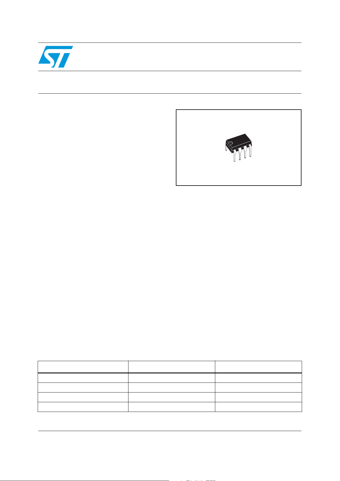
DIP-8
The TDE1767, TDE1767A, TDE1787, TDE1787A
are a monolithic amplifiers designed for high
current and high voltage applications, specifically
to drive lamps, relays, stepping motors.
The devices are assentially blow-out proof. The
output is prois protected from short-circuits with
the positive supply or drive. In addition thermal
shut down is provited to keep the IC from
overheathing.
If internal dissipation becomes too high, the driver
will shut down to prevent excessive heating. The
output stays null after the overheating is off, if the
reset input is low. If high the output will
alternatively switch-on and off until the overload is
removed.
Table 1. Device summary
Part number Package Packaging
TDE1767DP DIP8 Tube
TDE1767ADP DIP8 Tube
The devices operates over a wide range voltages
from standard 15V operational amplifier supplies
to the single +6V or +48V used for industrial
electric systems. Input voltages can be higher
than in the V
CC
.
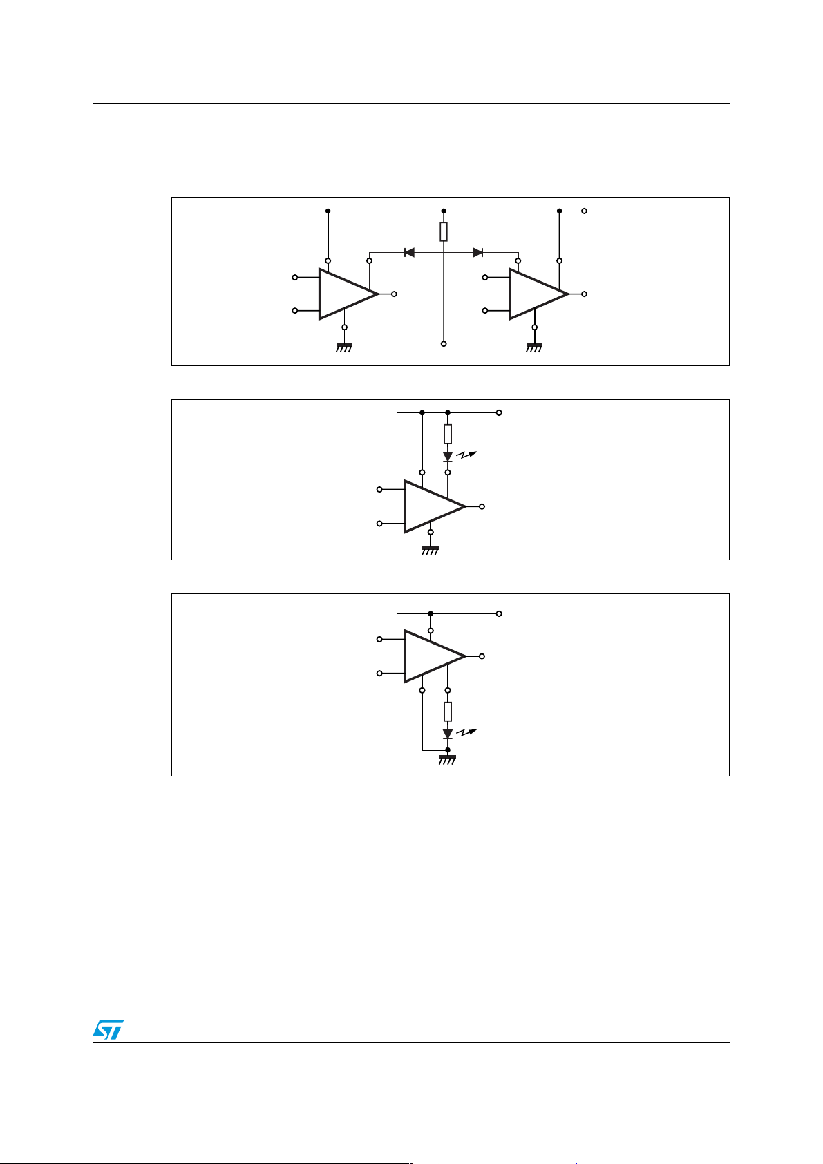
An alarm output suitable for driving a LED is
provited. This LED, normally on (if referred to
ground), will die out or flash during an overload
depending on the state of the reset input.
The output is low in open ground conditions.
TDE1787DP DIP8 Tube
TDE1787ADP DIP8 Tube
March 2007 Rev 2 1/16
www.st.com
16
Page 2

Contents TDE1767 - TDE1787
Contents
1 Pin connections . . . . . . . . . . . . . . . . . . . . . . . . . . . . . . . . . . . . . . . . . . . . . 3
2 Maximum ratings . . . . . . . . . . . . . . . . . . . . . . . . . . . . . . . . . . . . . . . . . . . . 3
2.1 Absolute maximum ratings . . . . . . . . . . . . . . . . . . . . . . . . . . . . . . . . . . . . . 3
2.2 Thermal data . . . . . . . . . . . . . . . . . . . . . . . . . . . . . . . . . . . . . . . . . . . . . . . 3
3 Electrical characteristcs . . . . . . . . . . . . . . . . . . . . . . . . . . . . . . . . . . . . . . 4
4 Schematic diagrams . . . . . . . . . . . . . . . . . . . . . . . . . . . . . . . . . . . . . . . . . 6
5 Typical characteristics . . . . . . . . . . . . . . . . . . . . . . . . . . . . . . . . . . . . . . . 7
6 Typical application . . . . . . . . . . . . . . . . . . . . . . . . . . . . . . . . . . . . . . . . . . 9
7 Using alarm output . . . . . . . . . . . . . . . . . . . . . . . . . . . . . . . . . . . . . . . . . 11
8 Mechanical data . . . . . . . . . . . . . . . . . . . . . . . . . . . . . . . . . . . . . . . . . . . . 13
9 Revision history . . . . . . . . . . . . . . . . . . . . . . . . . . . . . . . . . . . . . . . . . . . 15
2/16
Page 3

TDE1767 - TDE1787 Pin connections
1 Pin connections
Figure 1. Pin connection (top view)
ALARM OUTPUT
INVERTING INPUT
NON INVERTING INPUT
GND
2 Maximum ratings
2.1 Absolute maximum ratings
Table 2. Absolute maximum ratings
Symbol Parameter
VCC Supply voltage 60 50 V
V
V
l(reset)
I
P
T
oper
T
Input differential voltage 60 50 V
ID
V
Input voltage - 10 to + 60 - 10 to + 50 V
l
Output current 1.3 1.2 A
I
O
Reset input voltage - 0.5 to + 60 - 0.5 to + 50 V
Alarm output current - 10 to + 20 - 10 to + 20 mA
OA
Power dissipation Internally Limited mW
tot
Operating ambient temperature
range
Storage temperature range - 65 to + 150 - 65 to + 150 °C
stg
1
2
3
4 RESET
D03IN1475
TDE1767A
TDE1787A
CURRENT LIMIT8
V
7
CC
OUTPUT
6
5
TDE1767
TDE1787
- 25 to + 85 - 25 to + 85 °C
Unit
2.2 Thermal data
Table 3. Thermal data
Symbol Parameter Value Unit
R
th(JC)
R
th(JA)
Note: Devices bonded on a 40 cm2 glass-epoxy printed circuit 0.15 cm thick with 4 cm2 of copper.
Thermal resistance junction-case max 30 °C/W
Thermal resistance junction-ambient max 80 °C/W
3/16
Page 4
Electrical characteristcs TDE1767 - TDE1787
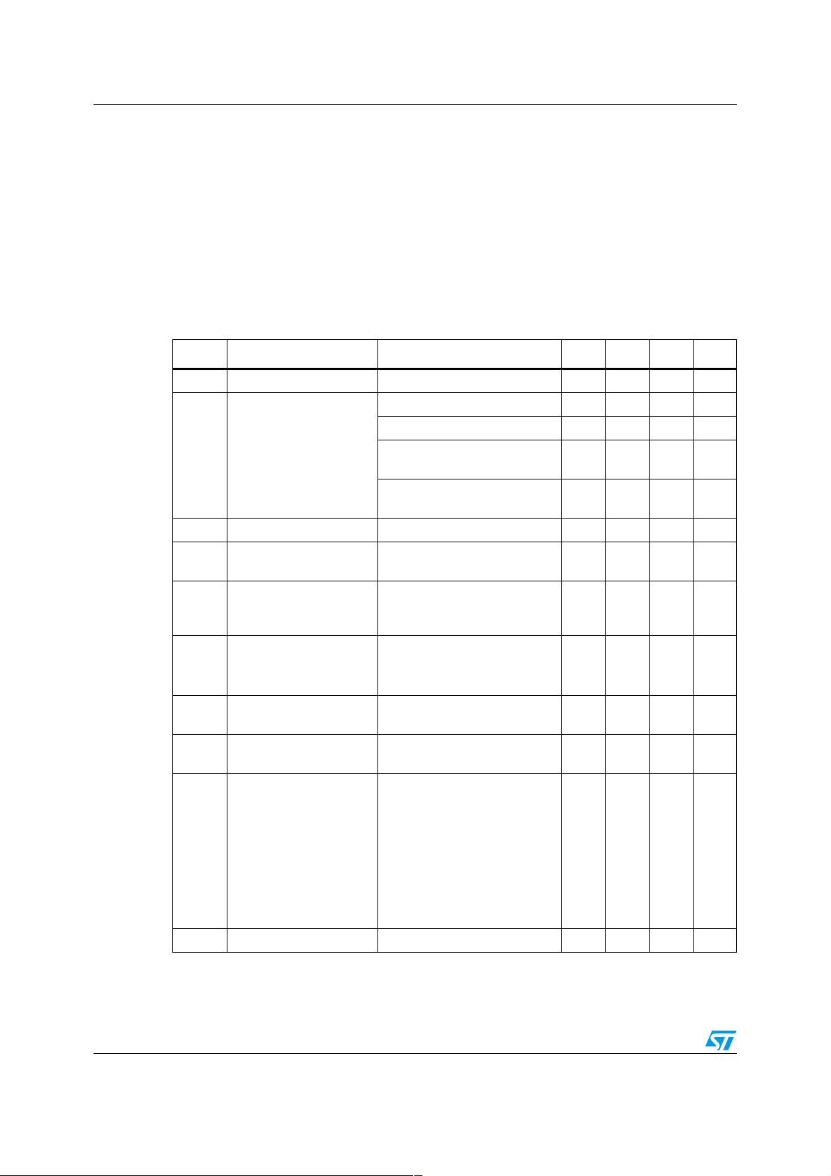
3 Electrical characteristcs
TDE1767A: - 25°C ≤ TA ≤ 85°C, 6V ≤ VCC ≤ 55V, Io ≤ 500mA, TJ ≤ 150°C
TDE1767: - 25°C ≤ T
TDE1787A: - 25°C ≤ T
TDE1787: 25°C ≤ T
≤ 85°C, 6V ≤ VCC ≤ 45V, Io ≤ 500mA, TJ ≤ 150°C
A
≤ 85°C, 6V ≤ VCC ≤ 55V, Io ≤ 300mA, TJ ≤ 150°C
A
≤ 85°C, 6V ≤ VCC ≤ 45V, Io ≤ 300mA, TJ ≤ 150°C
A
Unless otherwise specified.
Table 4. Electrical characteristics
Symbol Parameter Test condition Min. Typ. Max. Unit
V
Input offset voltage (note 1) 2 50 mV
IO
(measured on pin 4)
= 25°C) 5.8 8 mA
A
CCmax
CCmax
, (TJ = 150°C)
, (TA = 25°C)
57mA
1.5 4 mA
1
1
1
1
= 0.22Ω
SC
= 0.33Ω
SC
700
380
60
45
60
45
mA
mA
V
V
Output high (T
Power supply current
I
CC
Output high
(V
= V
CC
Output low
(V
= V
CC
Imput bias current 15 100 µA
I
IB
Common-mode input
CM
voltage range
V
Input voltage range
I
TDE1787A, TDE1767A
TDE1787, TDE1767
Vref
≥ 1V (figure1, note2)
TDE1787A, TDE1767A
TDE1787, TDE1767
= 35V, t = 10ms
V
Short circuit output
I
SC
current
Output limit sense
sense
voltage
CC
TDE1767A: R
TDE1787A: R
V
= VCC -2V, t = 10ms 130 150 170 mV
O
V
V
V
V
V
Output limit sense
sense
voltage
= 0V, t = 10ms 120 140 165 mV
V
O
Output high V
= 0; VCC = 30V
R
SC
TDE1787A, TDE1767A:
TJ = 25°C
V
O(sat)
Output saturation voltage
TDE1787, TDE1767: T
TDE1787A, TDE1767A:
= 150°C
T
J
TDE1787, TDE1767:
= 150°C
T
J
Output leakage current Output low 100 µA
I
OL
4/16
+
- V
I
-
≥ 50mV;
I
= 25°C
J
1
1
1.1
1.1
1.1
1.2
1.2
1.3
V
V
V
V
Page 5
TDE1767 - TDE1787 Electrical characteristcs
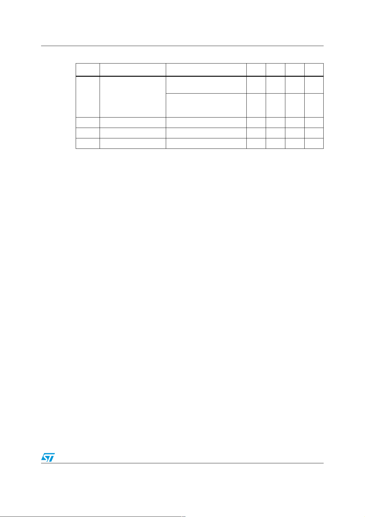
Table 4. Electrical characteristics (continued)
Symbol Parameter Test condition Min. Typ. Max. Unit
I
I
reset
V
th-reset
Output source current
= VCC-2.5V
V
Available alarm output
A
current
AH
Output sink current
(in thermal shut-down)
= 1.4V
V
A
Reset input current 2 40 µA
Reset threhold 1.4 A
-4 -5 mA
510 mA
Output leakage current open ground 10 µA
Note: 1 The offset voltage given is the maximum value of different input voltage reguired to drive the
output voltage whitin 2 V of the ground or the supply voltage.
2 Input voltage range is indipendent of the supply voltage.
5/16
Page 6
Schematic diagrams TDE1767 - TDE1787
8
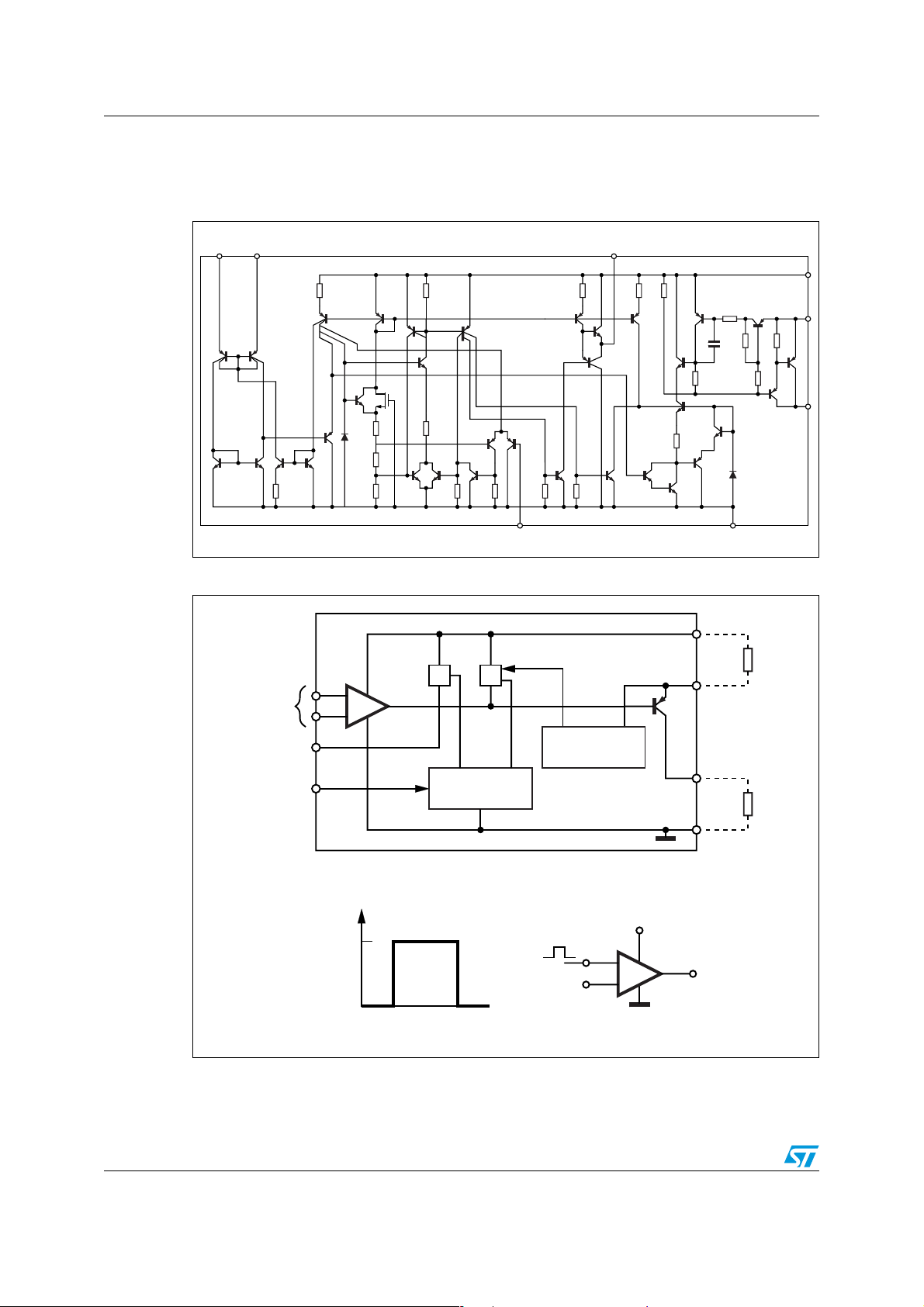
4 Schematic diagrams
Figure 2. Schematic diagram
+-
3 1
2
600
210Ω
3KΩ 2KΩ
20
Ω
KΩ
5KΩ
300
20
Ω
pF
2KΩ 2KΩ
200
7
8
Ω
3.6KΩ
1.1KΩ
8.4KΩ
300Ω
Figure 3. Equivalent schematic
G1 G2
ALARM OUTPUT
RESET
2
3INPUTS
1
5
AMP
-
+
10
KΩ
20KΩ20
KΩ
THERMAL
PROTECTION
6
1.8
KΩ
10
KΩ
54
3
KΩ
D03IN1476
7
V
CC
R
SC
8
CURRENT LIMIT
SHORT-CIRCUIT
PROTECTION
6 OUTPUT
R
L
4
GROUND
D03IN1477
V
l
1V
l(max)
0
The reference input can be the inverting or non-inverting one
6/16
V
REF
≥1V
V
+6V<VCC<V
CC
2
3
CC(max)
E
E
D03IN147
Page 7
TDE1767 - TDE1787 Typical characteristics
5 Typical characteristics
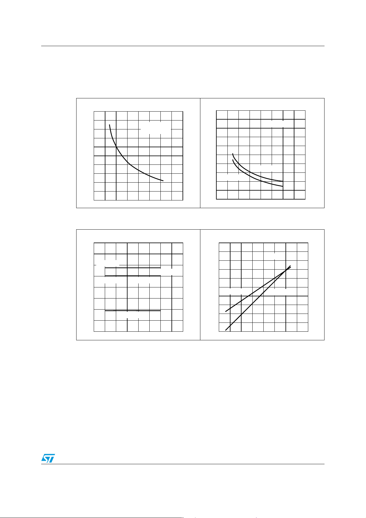
Figure 4. Peak short-circuit vs limiting
I
CS
(A)
0.9
0.8
0.7
0.6
0.5
0.4
0.3
0.2
0.1
resistor
V
T
CC
amb
= +30V
= +25˚C
D03IN1479
Figure 5. Available output current vs
limiting resistor
I
(A)
0.9
0.8
0.7
0.6
0.5
0.4
0.3
0.2
0.1
O
V
CC
T
= +25˚C
amb
T
= +85˚C
amb
D03IN1480
= +30V
000.1
0.2
0.3
0.4
0.5
0.6
0.7
RL(Ω)
000.1
0.2
0.3
0.4
0.5
0.6
0.7
RL(Ω)
Figure 6. Power supply current (pin 4) Figure 7. Output saturation voltage vs
I
S
(mA)
Tj = +25˚C
Tj = +150˚C
Output high
Output low
D03IN1481
IO = 0.5A
0010 20230 40 50 604706VS(V)
V
O (sat)
(V)
1.4
1.3
1.2
1.1
1.0
0.9
0.8
0.7
0.6
0.5
output current
Tj = +25˚C
0
0.1
0.2
0.3
0.4
R
= 0
SC
Tj = +150˚C
0.5
0.6
D03IN1482
0.7
IO(A)
7/16
Page 8
Typical characteristics TDE1767 - TDE1787
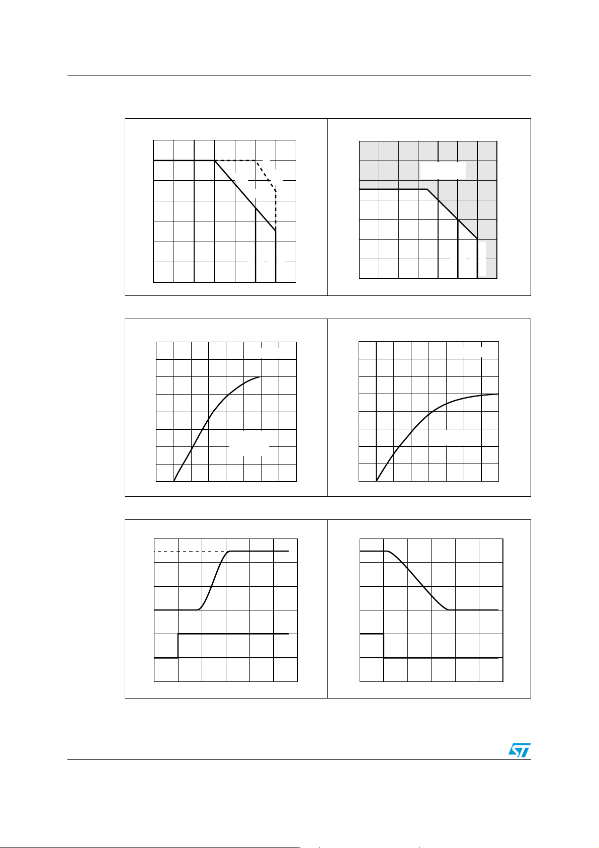
Figure 8. Output transistor safe
I
O
(A)
1.2
1.0
0.8
0.6
0.4
0.2
0
Figure 10. Current sinking Figure 11. Current sourcing
I
sync
(mA)
28
24
operating area (pulsed))
0
10
20
30
t = 100ms
40
t = 10ms
TDE1767
TDE1787
50
T
= +25˚C
amb
D03IN1483
TDE1787A
TDE1767A
60 VS(V)
D03IN1485
Figure 9. Normal operating area (short
circuit protected)
R
L
(Ω)
no short circuit
20
protection
30
40
TDE1767
50
T
amb
0.1
0.2
0.3
0.4
0.5
0.6
I
sync
(mA)
14
12
0
10
D03IN1484
TDE1787
TDE1787A
TDE1767A
60 VS(V)
D03IN1486
= +25˚C
20
16
12
8
Alarm output
after thermal
shutdown
4
0
0
Figure 12. Response time Figure 13. Response time
V
o
(V)
1
23
D03IN1487
(V)
V
O
0
V
i
(V)
0
10
V
(V)
2.5V
V
(V)
8
6
4
Alarm output
normal operation
2
0
0
o
1
23
0
i
0
V
D03IN1488
(V)
O
0
1234t(µs)
8/16
0
5101520t(µs)
Page 9
TDE1767 - TDE1787 Typical application
6 Typical application
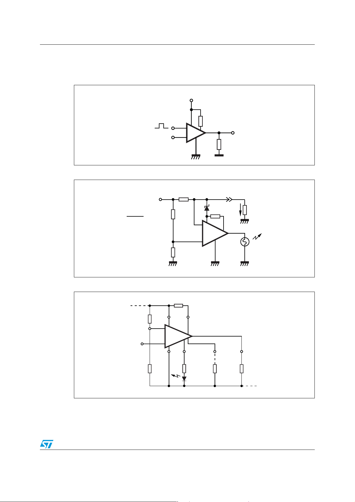
Figure 14. Test circuit
V
+30V
CC
0.22Ω
+
1.4V
D03IN1489
Figure 15. Open load detection.4
V
CC
VCCR
1
≥ 50mV
R
2
≥ 100mV
R
SIL
100Ω
R
S
LOADI
R
R
1
SC
+
-
R
2
L
D03IN1492
Figure 16. Driving lamps, relays, etc...
R
SC
V
CC
-
INPUT
GROUND
+
CURRENT LIMITING
ALARM
OUTPUT
5.6KΩ 100KΩ
RESET OUTPUT
(max)
R
L
D03IN1493
9/16
Page 10
Typical application TDE1767 - TDE1787
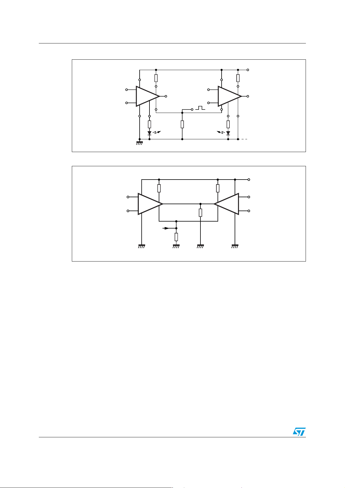
Figure 17. Common reset.
V
R
SC
CC
R
SC
-
RESET
ALARM
OUTPUT
RESET
100KΩ
(max)
++
GROUND
Figure 18. Parallel driving of loads up to 1 A.
0.15Ω 0.15Ω
V
ref
V
-
++
i
RESET
100KΩ
(max)
D03IN1494
R
L
D03IN1495
-
V
CC
-
V
ref
V
i
10/16
Page 11
TDE1767 - TDE1787 Using alarm output
7 Using alarm output
Figure 19. Parallel alarm output
V
CC
10KΩ
71 71
-
++
4
-
4
Figure 20. LED to VCC
Figure 21. LED to ground
ALARM SIGNAL
5.6KΩ
71
4
7
14
5.6KΩ
D03IN1497
D03IN1496
V
CC
V
CC
D03IN1498
11/16
Page 12
Using alarm output TDE1767 - TDE1787
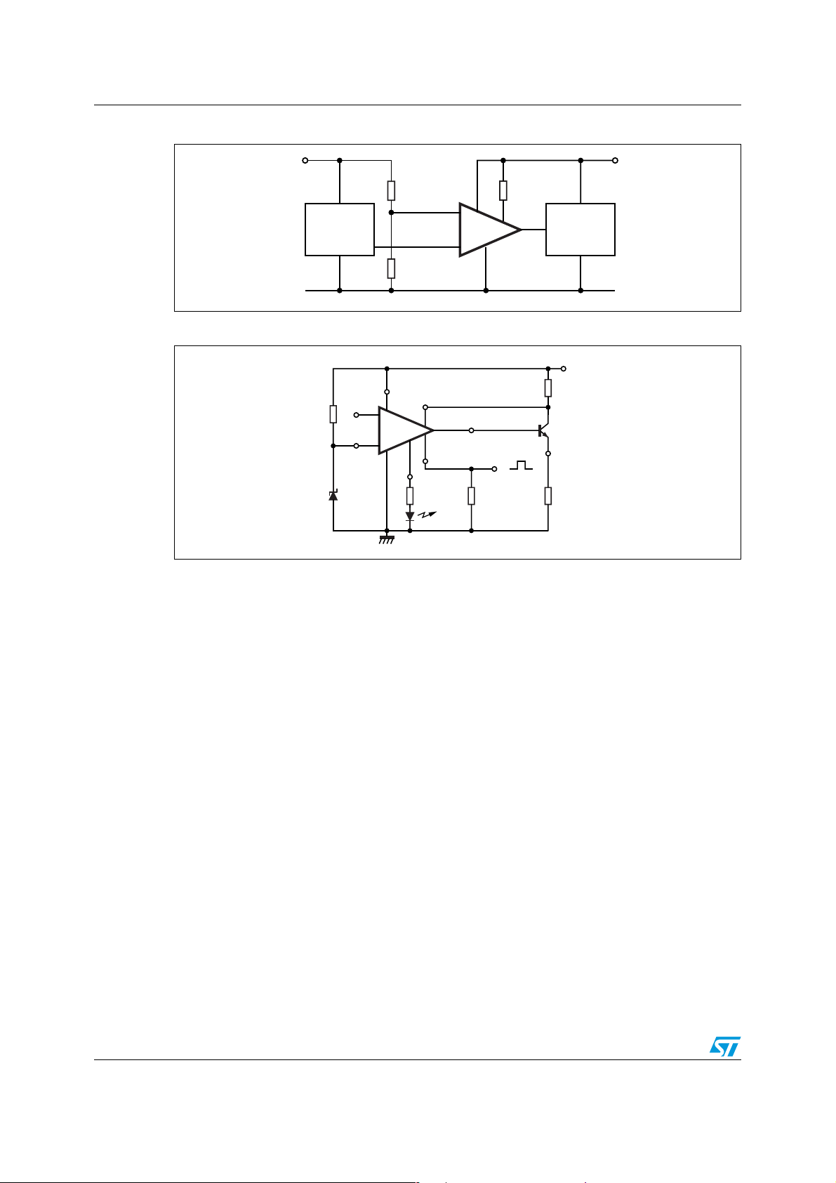
Figure 22. Interface between high voltage and low voltage system.
VCC≥+6VVCC≤+50V
R
SC
+1<V
<+50
I
HIGH
VOLTAGE
SYSTEM
0<V
<+50
I
LOW
VOLTAGE
SYSTEM
D03IN1499
Figure 23. Increasing current up to 10A.
V
CC
V
CC
CURRENT LIMITING
-
+
OUTPUT
RESET RESET
ALARM
OUTPUT
100KΩ
(max)
0.01Ω
R
L
GROUND
D03IN1500
12/16
Page 13

TDE1767 - TDE1787 Mechanical data
8 Mechanical data
In order to meet environmental requirements, ST offers these devices in ECOPACK®
packages. These packages have a Lead-free second level interconnect. The category of
second Level Interconnect is marked on the package and on the inner box label, in
compliance with JEDEC Standard JESD97. The maximum ratings related to soldering
conditions are also marked on the inner box label. ECOPACK is an ST trademark.
ECOPACK specifications are available at: www.st.com.
13/16
Page 14
Mechanical data TDE1767 - TDE1787
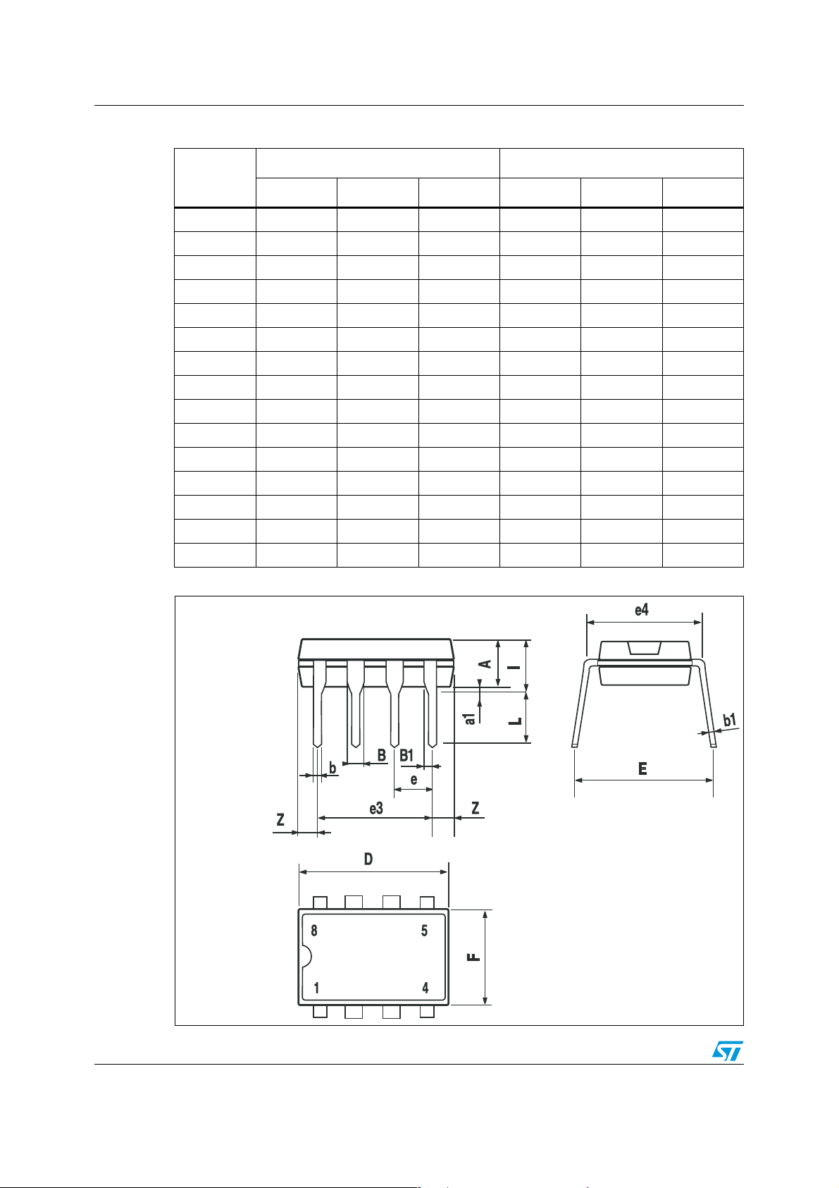
Table 5. DIP-8 Mechanical data
mm Inch
Dim.
Min Typ Max Min Typ Max
A 3.32 0.131
a1 0.51 0.020
B 1.15 1.65 0.045 0.065
b 0.356 0.55 0.014 0.022
b1 0.204 0.304 0.008 0.012
D 10.92 0.430
E 7.95 9.75 0.313 0.384
e 2.54 0.100
e3 7.62 0.300
e4 7.62 0.300
F 6.6 0.260
I 5.08 0.200
L 3.18 3.81 0.125 0.150
Z 1.52 0.060
Figure 24. Package dimensions
14/16
Page 15

TDE1767 - TDE1787 Revision history
9 Revision history
Table 6. Revision history
Date Revision Changes
20-Sep-2003 1 Initial release.
3-Mar-2007 2 Document reformatted, typo Figure 1 on page 3
15/16
Page 16

TDE1767 - TDE1787
Please Read Carefully:
Information in this document is provided solely in connection with ST products. STMicroelectronics NV and its subsidiaries (“ST”) reserve the
right to make changes, corrections, modifications or improvements, to this document, and the products and services described herein at any
time, without notice.
All ST products are sold pursuant to ST’s terms and conditions of sale.
Purchasers are solely responsible for the choice, selection and use of the ST products and services described herein, and ST assumes no
liability whatsoever relating to the choice, selection or use of the ST products and services described herein.
No license, express or implied, by estoppel or otherwise, to any intellectual property rights is granted under this document. If any part of this
document refers to any third party products or services it shall not be deemed a license grant by ST for the use of such third party products
or services, or any intellectual property contained therein or considered as a warranty covering the use in any manner whatsoever of such
third party products or services or any intellectual property contained therein.
UNLESS OTHERWISE SET FORTH IN ST’S TERMS AND CONDITIONS OF SALE ST DISCLAIMS ANY EXPRESS OR IMPLIED
WARRANTY WITH RESPECT TO THE USE AND/OR SALE OF ST PRODUCTS INCLUDING WITHOUT LIMITATION IMPLIED
WARRANTIES OF MERCHANTABILITY, FITNESS FOR A PARTICULAR PURPOSE (AND THEIR EQUIVALENTS UNDER THE LAWS
OF ANY JURISDICTION), OR INFRINGEMENT OF ANY PATENT, COPYRIGHT OR OTHER INTELLECTUAL PROPERTY RIGHT.
UNLESS EXPRESSLY APPROVED IN WRITING BY AN AUTHORIZED ST REPRESENTATIVE, ST PRODUCTS ARE NOT
RECOMMENDED, AUTHORIZED OR WARRANTED FOR USE IN MILITARY, AIR CRAFT, SPACE, LIFE SAVING, OR LIFE SUSTAINING
APPLICATIONS, NOR IN PRODUCTS OR SYSTEMS WHERE FAILURE OR MALFUNCTION MAY RESULT IN PERSONAL INJURY,
DEATH, OR SEVERE PROPERTY OR ENVIRONMENTAL DAMAGE. ST PRODUCTS WHICH ARE NOT SPECIFIED AS "AUTOMOTIVE
GRADE" MAY ONLY BE USED IN AUTOMOTIVE APPLICATIONS AT USER’S OWN RISK.
Resale of ST products with provisions different from the statements and/or technical features set forth in this document shall immediately void
any warranty granted by ST for the ST product or service described herein and shall not create or extend in any manner whatsoever, any
liability of ST.
ST and the ST logo are trademarks or registered trademarks of ST in various countries.
Information in this document supersedes and replaces all information previously supplied.
The ST logo is a registered trademark of STMicroelectronics. All other names are the property of their respective owners.
© 2007 STMicroelectronics - All rights reserved
STMicroelectronics group of companies
Australia - Belgium - Brazil - Canada - China - Czech Republic - Finland - France - Germany - Hong Kong - India - Israel - Italy - Japan -
Malaysia - Malta - Morocco - Singapore - Spain - Sweden - Switzerland - United Kingdom - United States of America
www.st.com
16/16
 Loading...