

Page 1

INTEGRATED CIRCUITS
DATA SH EET
TDA9880T
Alignment-freemultistandardvision
and FM sound IF-PLL demodulator
Product specification
Supersedes data of 1999 Jul 21
File under Integrated Circuits, IC02
2000 Nov 22
Page 2

Philips Semiconductors Product specification
Alignment-free multistandardvisionand
FM sound IF-PLL demodulator
FEATURES
• 5 V supply voltage
• Gain controlled wide-band Vision Intermediate
Frequency (VIF) amplifier (AC-coupled)
• True synchronous demodulation with active carrier
regeneration (very linear demodulation, good
intermodulation figures, reduced harmonics and
excellent pulse response)
• Fully integrated VIF Voltage Controlled Oscillator
(VCO), alignment-free
• Digital acquisition help, VIF frequencies of 38.0, 38.9,
45.75 and 58.75 MHz
• 4 MHz reference frequency input [signal from
Phase-Locked Loop (PLL) tuning system] or operating
as crystal oscillator
• VIF Automatic Gain Control (AGC) detector for gain
control, operating as peak sync detector, fast reaction
time
TDA9880T
• Precise fullydigital Automatic Frequency Control (AFC)
detector with 4-bit digital-to-analog converter
• Fully integrated sound carrier trap for 4.5, 5.5,
6.0 and 6.5 MHz, controlled by reference signal
• Alignment-freeselectiveFM-PLL demodulator with high
linearity and low noise
• Digital frequency control, sound carrier frequencies
4.5, 5.5, 6.0 and 6.5 MHz
• Stabilizer circuit for ripple rejection and to achieve
constant output signals
• Electrostatic discharge (ESD) protection for all pins.
GENERAL DESCRIPTION
The TDA9880T is an integrated circuit for multistandard
vision IF signal processing and FM demodulation in TV
and VTR sets.
ORDERING INFORMATION
TYPE NUMBER
NAME DESCRIPTION VERSION
TDA9880T SO20 plastic small outline package; 20 leads; body width 7.5 mm SOT163-1
PACKAGE
2000 Nov 22 2
Page 3

Philips Semiconductors Product specification
Alignment-free multistandard vision and
TDA9880T
FM sound IF-PLL demodulator
QUICK REFERENCE DATA
SYMBOL PARAMETER CONDITIONS MIN. TYP. MAX. UNIT
V
P
I
P
V
i(sens)(VIF)(rms)
G
VIF(cr)
f
VIF
∆f
VIF
V
o(v)(p-p)
G
dif
ϕ
dif
B
v(−3dB)(trap)
α
SC1
S/N
W
PSRR
13
B
v(−1dB)
I
ch(max)(20)
I
dch(max)(20)
I
sink(14)
AFC
stps
I
o(source)(19)
I
o(sink)(19)
V
o(intc)(rms)
supply voltage note 1 4.5 5.0 5.5 V
supply current 85 100 115 mA
VIF input voltage sensitivity
−1 dB video at output − 50 100 µV
(RMS value)
VIF gain control range see Fig.3 65 69 − dB
VIF frequencies see Table 2 − 38.0 − MHz
− 38.9 − MHz
− 45.75 − MHz
− 58.75 − MHz
VIF frequency window of digital
referenced to f
VIF
−±2.38 − MHz
acquisition help
video output signal voltage
(peak-to-peak value)
sound carrier off; see Fig.9 1.7 2.0 2.3 V
trap bypass mode;
0.95 1.10 1.25 V
see Fig.9
differential gain
differential phase
−3 dB video bandwidth including
sound carrier trap
“NTC-7 Composite”
“NTC-7 Composite”
CL< 20 pF; RL>1kΩ;
AC load; note 2
f
= 4.5 MHz
trap
− 25%
− 2 4 deg
3.95 4.05 − MHz
(M/N standard)
f
= 5.5 MHz
trap
4.90 5.00 − MHz
(B/G standard)
trap attenuation at first sound carrier M/N standard 30 36 − dB
B/G standard 30 36 − dB
weighted signal-to-noise ratio of
see Fig.5; note 3 56 60 − dB
video signal
power supply ripple rejection at
pin 13
−1 dB video bandwidth CL< 20 pF; RL>1kΩ;
f
= 70 Hz; video signal;
ripple
grey level; see Fig.8
25 28 − dB
56−MHz
AC load; trap bypass mode
AGC maximum charge current at
6810µA
pin 20
AGC maximum discharge current at
7.5 10 12.5 µA
pin 20
sink current of tuner AGC at pin 14 maximum tuner gain
450 600 750 µA
reduction; V14=1V;
see Fig.3
AFC steepness ∆I19/∆f 0.85 1.05 1.25 µA/kHz
AFC output source current at pin 19 160 200 240 µA
AFC output sink current at pin 19 160 200 240 µA
intercarrier output voltage
(RMS value)
V
i(SC)
-------------V
i(PC)
note 4
24 dB;–=
− 49 − mV
2000 Nov 22 3
Page 4

Philips Semiconductors Product specification
Alignment-free multistandard vision and
TDA9880T
FM sound IF-PLL demodulator
SYMBOL PARAMETER CONDITIONS MIN. TYP. MAX. UNIT
B
intc(−3dB)(ul)
V
o(AF)(8)(rms)
THD
8
B
AF(−3dB)
S/N
W(AF)
α
AM(sup)
PSRR
8
∆f
FM
f
ref(15)
V
ref(15)(rms)
upper limit −3 dB intercarrier
7.5 9.0 − MHz
bandwidth
audio output signal voltage at pin 8
(RMS value)
25 kHz FM deviation;
75 µs de-emphasis
400 500 600 mV
total harmonic distortion at pin 8 − 0.15 0.5 %
−3 dB audio frequency bandwidth without de-emphasis;
100 120 − kHz
dependent on loop filter at
pin 4
weighted signal-to-noise ratio of
audio signal
black picture 50 56 − dB
white picture 45 51 − dB
6 kHz sine wave
40 46 − dB
(black-to-white modulation)
sound carrier
35 40 − dB
subharmonics;
f = 2.25 MHz ±3 kHz
AM suppression of FM demodulator 75 µs de-emphasis;
40 46 − dB
AM: f = 1 kHz; m = 0.3
referenced to 25 kHz
FM deviation
power supply ripple rejection at pin 8 f
frequency window of digital
= 70 Hz; see Fig.8 14 20 − dB
ripple
−±225 − kHz
acquisition help for FM demodulator
frequency of reference signal at
− 4.0 − MHz
pin 15
amplitude of referencesignal source
operation as input terminal 80 − 400 mV
at pin 15 (RMS value)
Notes
1. Values of video and sound parameters can be decreased at VP= 4.5 V.
2. The sound carrier frequencies (depending on TV standard) are attenuated by the integrated sound carrier traps
(see Figs 12 to 17); H (s) is the absolute value of transfer function.
3. S/N is the ratio of black-to-white amplitude to the black level noise voltage (RMS value, pin 13). B = 4.2 MHz
(M/N standard) or B = 5.0 MHz (B/G, I and D/K standard) weighted in accordance with
“CCIR 567”
.
4. The intercarrier output signal at pin 11 can be calculated by the following formula taking into account the internal
video signal with 1.1 V (p-p) as a reference:
V
iSC()
dB()6 dB 3 dB±+
--------------V
iPC()
V
o(intc)(rms)
1.1 V (p-p)
1
× 10
---------- 22
--------------------------------------------------------------- -
×=
20
where:
1
= correction term for RMS value, = sound-to-picture carrier ratio at VIF input (pins 1 and 2) in dB,
---------- 22
V
iSC()
--------------V
iPC()
dB()
6 dB = correction term of internal circuitry and ±3 dB = tolerance of video output and intercarrier output amplitude
V
o(intc)(rms)
.
2000 Nov 22 4
Page 5
This text is here in white to force landscape pages to be rotated correctly when browsing through the pdf in the Acrobat reader.This text is here in
d
_white to force landscape pages to be rotated correctly when browsing through the pdf in the Acrobat reader.This text is here inThis text is here in
white to force landscape pages to be rotated correctly when browsing through the pdf in the Acrobat reader. white to force landscape pages to be ...
2000 Nov 22 5
book, full pagewidth
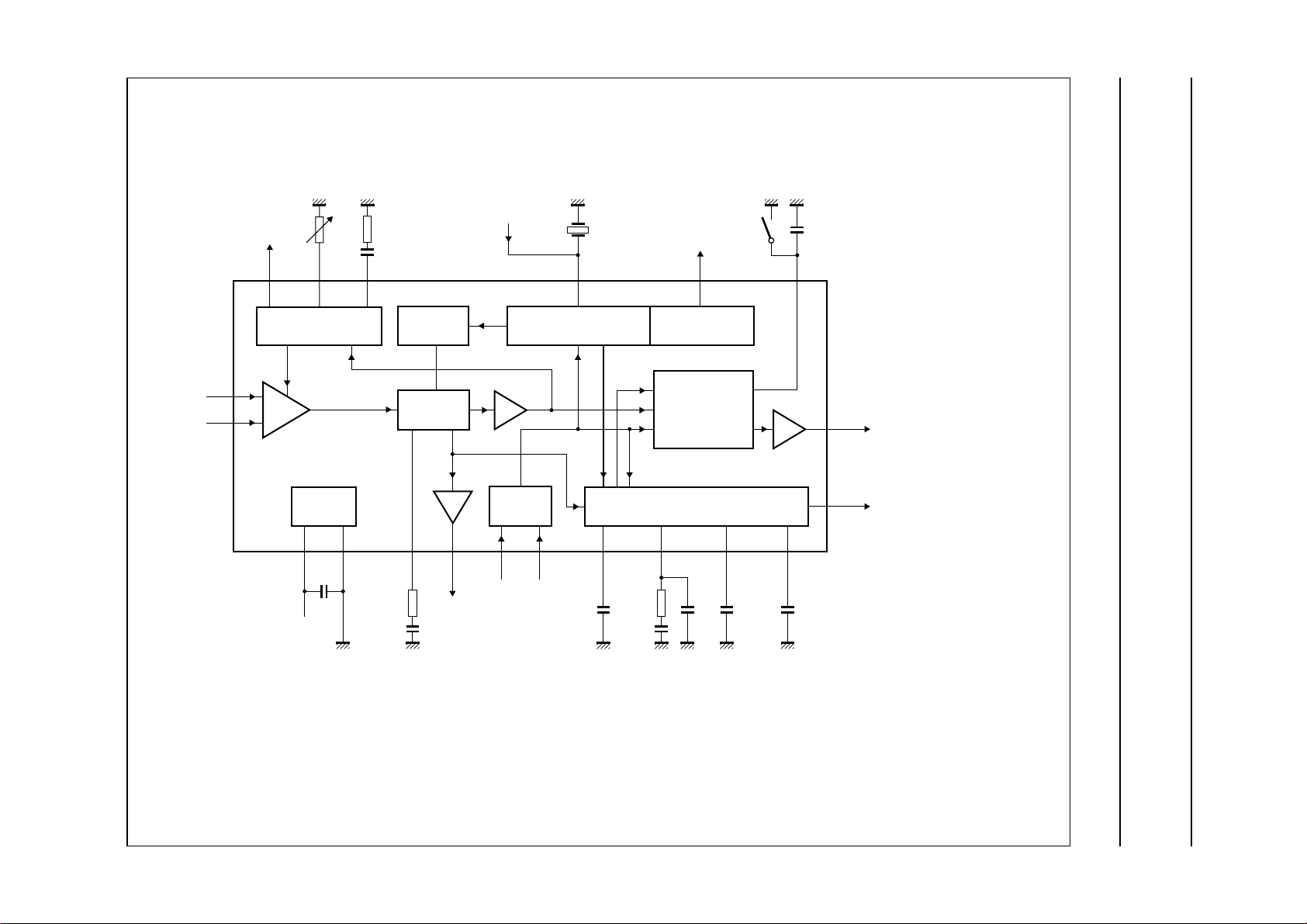
BLOCK DIAGRAM
Philips Semiconductors Product specification
Alignment-free multistandard vision and
FM sound IF-PLL demodulator
VIF1
VIF2
external reference
or 4 MHz crystal
R
TOP
C
VAGC
TAGC
14 3 20 15 19 12
1
2
TOP
AGC
VAGC
RC VCO
VIF-PLL
DIGIT AL VCO CONTROL AFC DETECTOR
REF
SOUND TRAPS
trap disable
switch
AFC
4.5 to 6.5 MHz
TDA9880T
SUPPL Y
VPLLVPGND
sound
intercarrier
output
SIO
LOGIC
911181617
S1S0
NARROW-BAND FM-PLL DETECTOR
FAGC
C
FMPLL DEEM AFD
FAGC
C
DEEM
C
TR
TR
CVBS
13
8
AUD
645710
C
AFD
video output 2 V (p-p)
[1.1 V (p-p) without trap]
audio output
VIF-PLL
filter
FM-PLL
filter
Fig.1 Block diagram.
de-emphasis decoupling
MHB506
TDA9880T
Page 6

Philips Semiconductors Product specification
Alignment-free multistandard vision and
FM sound IF-PLL demodulator
PINNING
SYMBOL PIN DESCRIPTION
VIF1 1 VIF differential input 1
VIF2 2 VIF differential input 2
TOP 3 tuner AGC TakeOver Point (TOP)
FMPLL 4 FM-PLL filter
DEEM 5 de-emphasis capacitor
AFD 6 AF decoupling capacitor
FAGC 7 FM-PLL AGC capacitor
AUD 8 audio output
S0 9 switch input S0
S1 10 switch input S1
SIO 11 sound intercarrier output
TR 12 trap control
CVBS 13 video output
TAGC 14 tuner AGC output
REF 15 4 MHz crystal or reference input
GND 16 ground supply
V
P
VPLL 18 VIF-PLL filter
AFC 19 AFC output
VAGC 20 VIF-AGC capacitor
17 supply voltage (+5 V)
handbook, halfpage
VIF1
1
VIF2
2
TOP
3
FMPLL
4
DEEM
5
6
7
8
9
10
TDA9880T
MHB106
AFD
FAGC
AUD
S0
S1
Fig.2 Pin configuration.
TDA9880T
VAGC
20
19
AFC
18
VPLL
V
17
P
16
GND
15
REF
TAGC
14
CVBS
13
TR
12
SIO
11
2000 Nov 22 6
Page 7

Philips Semiconductors Product specification
Alignment-free multistandard vision and
FM sound IF-PLL demodulator
FUNCTIONAL DESCRIPTION
Figure 1 shows the simplified block diagram of the
integrated circuit. The integrated circuit comprises the
following functional blocks:
1. VIF amplifier
2. Tuner-AGC and VIF-AGC
3. VIF-AGC detector
4. Frequency Phase-Locked Loop (FPLL) detector
5. VCO and Travelling Wave Divider (TWD)
6. Digital acquisition help and AFC
7. Video demodulator and amplifier
8. Sound carrier trap
9. Intercarrier mixer
10. FM demodulator and acquisition help
11. Audio amplifier
12. Internal voltage stabilizer.
VIF amplifier
The VIF amplifier consists of three AC-coupled differential
amplifier stages. Each differential stage comprises a
feedback network controlled by emitter degeneration.
Tuner-AGC and VIF-AGC
The AGC capacitor voltage is converted to an internal VIF
gaincontrol signal, and is fedto the tuner AGC togenerate
the tuner AGC output current at pin TAGC (open-collector
output). The tuner AGC takeover point can be adjusted
with R
filter in order to achieve the optimum IF input level.
VIF-AGC detector
The AGC detector generates the required VIF gain control
voltage for constant video output by charging or
discharging the AGC capacitor. Gain control is performed
by sync level detection. The newly developed AGC circuit
provides fast reaction time to cope with ‘aeroplane
fluttering’. The time constants for decreasing or increasing
gain are nearly equal.
. This allows the tuner to be matchedto the SAW
TOP
TDA9880T
After frequency lock-in the phase detector produces a DC
current proportional to the phase difference between the
VCO and the input signal. The DC current of either the
frequency detector or the phase detector is converted into
aDCvoltagevia the VIF-PLL filter, which controls the VCO
frequency.
VCO and Travelling Wave Divider (TWD)
The Resistor Capacitor (RC) VCO operates as an
integrated relaxation oscillator atdouble the picture carrier
frequency.The control voltage required totunethe VCO to
actually double the picture carrier frequency is generated
by the FPLL detector and fed via the loop filter to the VCO
control input terminal.
The oscillator signal is divided-by-two with a TWD which
generatestwo differential output signals witha 90 degrees
phase difference independent of the frequency.
Digital acquisition help and AFC
The integrated relaxation oscillator has a very wide
frequency range from approximately 30 to 70 MHz (after
the TWD). To prevent false locking of the FPLL and with
respect to the catching range of the frequency detector of
maximum ±2.5 MHz, the Digital Acquisition Help (DAH)
provides current into the loop filter until the VCO is in a
frequency window of ±2.3 MHz around the wanted VIF
frequency. In this case the analog operating FPLL willlock
the VCO to the VIF carrier and the acquisition help does
not provide any current to the loop filter.
The principle of the digital acquisition help is as follows:
the VCO is connected to a downcounter, which is preset
depending on the required VIF frequency. The counting
time, as well as the counter control, is derived from a
4 MHz reference signal. This signal can be supplied from
the internal 4 MHz crystal oscillator or from the 4 MHz
reference oscillator of an external tuning system.
The counting result after a counting cycle corresponds to
the actual VCO frequency.
The digital AFC is also derived from the counting result
after a counting cycle by digital-to-analog converting the
last four bits of the counter.
Frequency Phase-Locked Loop (FPLL) detector
The VIF amplifier output signal is fed into a Frequency
Detector(FD) and into a PhaseDetector (PD) via a limiting
amplifier. During acquisition the frequency detector
produces a DC current proportional to the frequency
difference between the input and the VCO signal.
2000 Nov 22 7
Video demodulator and amplifier
The video demodulator is realized by a multiplier which is
designedforlowdistortionandlargebandwidth.Thevision
IF input signal is multiplied with the ‘in phase’ signal of the
travelling wave divider output.
Page 8

Philips Semiconductors Product specification
Alignment-free multistandard vision and
FM sound IF-PLL demodulator
The demodulator output signal is fed via an integrated
low-pass filter for attenuation of the carrier harmonics to
the video amplifier. The video amplifier is realized by an
operational amplifier with internal feedback and high
bandwidth. A low-pass filter is integrated to achieve an
attenuation of the carrier harmonics. The video signal of
1.1 V (p-p) for nominal vision IF modulation is fed
internally to the integrated sound carrier trap as well as to
the VIF-AGC detector. The second stage of the video
amplifier converts and amplifies the differential output
signal from the sound carrier trap to the single-ended
CVBS output signal at pin 13 with a 2 V (p-p) amplitude.
Noise clipping is provided. Furthermore the trap can be
bypassed by the implemented input switch of the second
amplifier stage, forced by connecting pin 12 to ground.
Sound carrier trap
The sound carrier trap consists of a reference filter, a
phase detector and the sound trap itself.
A sound carrier reference signal is fed into the reference
low-pass filter and is shifted by a nominal 90 degrees.
The phasedetectorcomparestheoriginalreferencesignal
with the signal shiftedby the reference filter and produces,
at the external capacitor CTR, a DC voltage by charging or
discharging the capacitor with a current proportional to the
phase difference between both signals, respectively to the
frequency error of the integrated filters. The DC voltage is
converted to currents which control the frequency position
of the reference filter and the sound trap.
The sound trap itselfis constructed of three separate traps
to realize sufficient suppression of the first and second
sound carrier. The right frequency position of the different
standards is set by the sound carrier reference signal.
Intercarrier mixer
The intercarrier mixer is realized by a multiplier, operating
inquadraturemodeforsuppressionoflowfrequencyvideo
signals. The VIF amplifier output signal is fed to the
intercarrier mixer and converted to an intercarrier
frequency by the regenerated 90 degree picture carrier
from the VCO. The mixer output signal is fed via a
band-pass filter and amplifier for attenuation of the high
frequency video signal components and carrier harmonics
to the output pin 11. The intercarrier signal is fed also to
the integrated FM demodulator.
TDA9880T
FM demodulator and acquisition help
The FM demodulator is realized as a narrow-band PLL
with external loop filter, which provides the necessary
selectivity. To achieve good selectivity, a linear phase
detector and constant input level are required. The
intercarrier signal from the intercarrier mixer is fed via a
gain controlled amplifier to the phase detector and it’s
output signal controls (via the loop filter) the integrated
relaxation oscillator. The possible frequency range is from
4 to 7 MHz. As a result of locking the oscillator frequency
tracks with the FM modulation of the input signal;
therefore,theoscillator control voltage is superimposed by
the AF voltage. In this way the FM-PLL operates as an
FM demodulator. The AF voltage is present at the loop
filter and is fed via a buffer with 0 dB gain to the audio
amplifier.
The digital acquisition help operates in the same way as
described in Section “Digital acquisition help and AFC”.
Audio amplifier
The audio amplifier consists of two parts:
1. The AF preamplifier is an operational amplifier with
internal feedback, high gain and high common mode
rejection. The AF voltage from the PLL demodulator,
by principle a small output signal, is amplified by
30 dB. A DC operating point control circuit (pin 6)
decouples the AF amplifier from the DC voltage of the
PLL. The low-pass characteristic of the amplifier
reduces the harmonics of the intercarrier signal at the
sound output terminal. If required, a de-emphasis
network can be realized by the amplifier output
resistance and an external capacitor.
2. The AF output amplifier (10 dB) provides the required
output level by a rail-to-rail output stage. This amplifier
makes use of an input selector for switching to mute
state, automatically controlled by the mute switching
voltage from the digital acquisition help in order to
avoid lock-in noise. During normal operation the
automatic audio mute function is not active.
Application of a 2.2 kΩ resistor between the
intercarrier output (pin 11) and ground will activate the
automatic audio mute function.
Internal voltage stabilizer
The band gap circuit internally generates a voltage of
approximately 2.4 V, independent of the supply voltage
and the temperature. Avoltage regulator circuit, controlled
by this voltage, produces a constant voltage of 3.55 V
which is used as an internal reference voltage.
2000 Nov 22 8
Page 9

Philips Semiconductors Product specification
Alignment-free multistandard vision and
TDA9880T
FM sound IF-PLL demodulator
LIMITING VALUES
In accordance with the Absolute Maximum Rating System (IEC 60134).
SYMBOL PARAMETER CONDITIONS MIN. MAX. UNIT
V
P
V
n
t
sc
T
stg
T
amb
V
es
Notes
1. Charge device model class A; machine model: discharging a 200 pF capacitor via a 0.75 µH inductance.
2. Charge device model class B; human body model: discharging a 100 pF capacitor via a 1.5 kΩ series resistor.
supply voltage IP= 115 mA; T
=70°C; at
amb
− 5.5 V
maximum chip temperature of 125 °C
voltage at
pins 1 to 4, 6 to 10, 12 and 17 to 20 0 V
P
V
pin 14 0 13.2 V
short-circuit time to ground or V
P
− 10 s
storage temperature −25 +150 °C
ambient temperature −20 +70 °C
electrostatic handling voltage for all
pins
note 1 −250 +250 V
note 2 −3000 +3000 V
THERMAL CHARACTERISTICS
SYMBOL PARAMETER CONDITIONS VALUE UNIT
R
th(j-a)
thermal resistance from junction to ambient in free air 85 K/W
2000 Nov 22 9
Page 10

Philips Semiconductors Product specification
Alignment-free multistandard vision and
TDA9880T
FM sound IF-PLL demodulator
CHARACTERISTICS
VP=5V; T
PC/SC = 10 dB) is used for specification; V
1 : 1; DSB video modulation; 10% residual carrier; video signal in accordance with
taken in test circuit of Fig.18; unless otherwise specified.
SYMBOL PARAMETER CONDITIONS MIN. TYP. MAX. UNIT
Supply (pin 17)
V
P
I
P
P
tot
VIF amplifier (pins 1 and 2)
V
i(sens)(VIF)(rms)
V
i(max)(rms)
∆V
int
G
VIF(cr)
B
VIF(−3dB)(ll)
B
VIF(−3dB)(ul)
R
i(dif)
C
i(dif)
V
I
FPLL and true synchronous video demodulator; note 4
f
VCO(max)
f
VIF
∆f
VIF
t
acq
V
i(sens)(VIF)(rms)
SIGNAL AT PIN 18
I
o(source)(PD)(max)
=25°C; see Table 2 for input frequencies; M standard (fPC= 45.75 MHz; fSC= 41.25 MHz;
amb
i(VIF)(rms)
= 10 mV (sync level); IF input from 50 Ω via broadband transformer
“NTC-7 Composite”
supply voltage note 1 4.5 5 5.5 V
supply current 85 100 115 mA
total power dissipation − 500 633 mW
VIF input voltage sensitivity
−1 dB video at output − 50 100 µV
(RMS value)
maximum input signal voltage
(RMS value)
internal IF amplitudedifference
between picture and sound
1 dB video at output;
note 2
within AGC range;
∆f = 4.5 MHz
110 −−mV
− 0.7 1 dB
carrier
VIF gain control range see Fig.3 65 69 − dB
lower limit −3 dB VIF
− 15 25 MHz
bandwidth
upper limit −3 dB VIF
70 100 − MHz
bandwidth
differential input resistance note 3 1.7 2.2 2.7 kΩ
differential input capacitance note 3 1.2 1.7 2.5 pF
DC input voltage − 3.35 − V
maximum oscillator frequency
f=2f
PC
120 140 − MHz
for carrier regeneration
vision carrier operating
frequencies
see Table 2 − 38.0 − MHz
− 38.9 − MHz
− 45.75 − MHz
− 58.75 − MHz
VIFfrequency window of digital
referenced to f
VIF
−±2.38 − MHz
acquisition help
acquisition time BL = 70 kHz; note 5 −−30 ms
VIF input voltage sensitivity at
pins 1 and 2 (RMS value)
for PLL to be locked maximum IF gain − 30 70 µV
for C/N = 10 dB notes 6 and 7 − 100 140 µV
maximum source current of
− 17 −µA
phase detector output
; measurements
2000 Nov 22 10
Page 11

Philips Semiconductors Product specification
Alignment-free multistandard vision and
TDA9880T
FM sound IF-PLL demodulator
SYMBOL PARAMETER CONDITIONS MIN. TYP. MAX. UNIT
I
o(sink)(PD)(max)
I
o(source)(DAH)
I
o(sink)(DAH)
t
W(min)(DAH)
K
O(VIF)
K
D(VIF)
Video output signal and sound carrier trap (pin 13; sound carrier off)
V
o(v)(p-p)
V
sync
V
zc
V
v(clu)
V
v(cll)
R
o
I
bias(int)
I
o(source)(max)
I
o(sink)(max)
∆V
o
∆V
o(bl)
G
dif
ϕ
dif
B
v(−3dB)(trap)
maximum sink current of
− 17 −µA
phase detector output
output source current of digital
− 23 −µA
acquisition help
output sink current of digital
− 23 −µA
acquisition help
minimum pulse width of digital
− 64 −µs
acquisition help current
VCO steepness ∆f
phase detector steepness
∆I18/∆ϕ
VIF
video output signal voltage
VIF
/∆V
18
− 20 − MHz/V
− 23 −µA/rad
see Fig.9 1.7 2.0 2.3 V
(peak-to-peak value)
sync pulse voltage level see Fig.9 1.15 1.35 1.55 V
zero carrier voltage level see Fig.9 3.27 3.57 3.87 V
upper video clipping voltage
VP− 1.1 VP− 1 − V
level
lower video clipping voltage
− 0.7 1.0 V
level
output resistance note 3 −−30 Ω
internal DC bias current for
2.0 2.5 − mA
emitter-follower
maximum AC and DC output
2.4 −−mA
source current
maximum AC and DC output
1.4 −−mA
sink current
deviation of CVBS output
signal voltage
50 dB gain control −−0.5 dB
30 dB gain control −−0.1 dB
black level tilt −−1%
differential gain
differential phase
−3 dB video bandwidth
including sound carrier trap
“NTC-7 Composite”
“NTC-7 Composite”
CL< 20 pF; RL>1kΩ;
AC load; note 8
f
= 4.5 MHz
trap
− 25%
− 2 4 deg
3.95 4.05 − MHz
(M/N standard)
f
= 5.5 MHz
trap
4.90 5.00 − MHz
(B/G standard)
= 6.0 MHz
f
trap
5.2 5.50 − MHz
(I standard)
f
= 6.5 MHz
trap
5.5 5.95 − MHz
(D/K standard)
2000 Nov 22 11
Page 12

Philips Semiconductors Product specification
Alignment-free multistandard vision and
TDA9880T
FM sound IF-PLL demodulator
SYMBOL PARAMETER CONDITIONS MIN. TYP. MAX. UNIT
α
SC1
α
SC1(60 kHz)
α
SC2
α
SC2(60 kHz)
t
d(g)(CC)
S/N
W
S/N
UW
αd
blue
αd
yellow
∆V
r(vc)(rms)
α
H(sup)
α
H(spur)
PSRR
13
trap attenuation at first sound
carrier
M/N standard 30 36 − dB
B/G standard 30 36 − dB
I standard 26 32 − dB
D/K standard 26 32 − dB
trap attenuation at first sound
carrier f
SC1
±60 kHz
M/N standard 21 27 − dB
B/G standard 24 30 − dB
I standard 20 26 − dB
D/K standard 20 26 − dB
trap attenuation at second
sound carrier
M/N standard 21 27 − dB
B/G standard 21 27 − dB
I standard 12 18 − dB
D/K standard 18 24 − dB
trap attenuation at second
sound carrier f
SC2
±60 kHz
M/N standard 15 21 − dB
B/G standard 15 21 − dB
I standard 10 15 − dB
D/K standard 13 18 − dB
group delay at chrominance
carrier frequency
3.58 MHz at
M/N standard
4.43 MHz at B/G standard 110 180 250 ns
4.43 MHz at I standard − 90 160 ns
4.28 MHz at D/K standard − 60 130 ns
weighted signal-to-noise ratio weighted in accordance
with
“CCIR 567”
;
see Fig.5; note 9
unweighted signal-to-noise
note 9 47 51 − dB
ratio
intermodulation attenuation at
‘blue’
f = 0.92 MHz; see Fig.6;
note 10
f = 2.76 MHz; see Fig.6;
note 10
intermodulation attenuation at
‘yellow’
f = 0.92 MHz; see Fig.6;
note 10
f = 2.76 MHz; see Fig.6;
note 10
residual vision carrier
(RMS value)
harmonics suppression in
video signal
spuriouselementssuppression
fundamental wave and
harmonics
CL< 20 pF; RL>1kΩ;
AC load; note 11a
note 11b 40 −−dB
in video signal
powersupply ripple rejectionat
pin 13
f
= 70 Hz; video
ripple
signal; grey level;
see Fig.8
110 180 250 ns
56 60 − dB
58 64 − dB
58 64 − dB
60 66 − dB
59 65 − dB
− 25mV
35 40 − dB
25 28 − dB
2000 Nov 22 12
Page 13

Philips Semiconductors Product specification
Alignment-free multistandard vision and
TDA9880T
FM sound IF-PLL demodulator
SYMBOL PARAMETER CONDITIONS MIN. TYP. MAX. UNIT
Video output signal (pin 13; trap bypass mode; V12< 0.8 V; sound carrier off); see Fig.9; note 12
V
o(v)(p-p)
video output signal voltage
(peak-to-peak value)
V
V
V
sync
zc
v(clu)
sync pulse voltage level 1.4 1.5 1.6 V
zero carrier voltage level 2.57 2.72 2.87 V
upper video clipping voltage
level
V
v(cll)
lower video clipping voltage
level
B
v(−1dB)
B
v(−3dB)
S/N
S/N
W
UW
−1 dB video bandwidth CL< 20 pF; RL>1kΩ;
−3 dB video bandwidth CL< 20 pF; RL>1kΩ;
weighted signal-to-noise ratio weighted in accordance
unweighted signal-to-noise
ratio
Trap control (pin 12)
I
o(source)(max)
maximum output source
current
I
o(sink)(max)
K
D(trap)
V
12
maximum output sink current 9 13 17 µA
frequency detector steepness
∆I12/∆f
trap
operating voltage range of trap
frequency control at pin 12
I
L(12)
CR
V
sw
I
source
stps
leakage current at pin 12 ∆f
control steepness ∆f
switching voltage trap bypass mode active −−0.8 V
source current trap bypass mode active;
VIF-AGC detector (pin 20)
I
ch(max)(20)
I
dch(max)(20)
t
res(inc)
maximum charge current 6 8 10 µA
maximum discharge current 7.5 10 12.5 µA
AGC response time to an
increasing VIF step
trap
/∆V
see Fig.9 0.95 1.10 1.25 V
3.1 3.25 − V
− 1.15 1.3 V
56−MHz
AC load
78−MHz
AC load
56 60 − dB
with
“CCIR 567”
;
see Fig.5; note 9
note 9 49 53 − dB
5913µA
f
= 4.5 MHz
trap
−−8−µA/MHz
(M/N standard)
f
= 6.5 MHz
trap
−−5.5 −µA/MHz
(D/K standard)
1.5 − 3.5 V
< ±25 kHz −−±80 nA
trap
f
12
= 4.5 MHz
trap
− 4.5 − MHz/V
(M/N standard)
= 6.5 MHz
f
trap
− 9 − MHz/V
(D/K standard)
− 185 −µA
V12≤ 0.8 V
6 dB; note 13 − 2.0 − ms
20 dB; note 13 − 2.5 − ms
40 dB; note 13 − 4.0 − ms
2000 Nov 22 13
Page 14

Philips Semiconductors Product specification
Alignment-free multistandard vision and
TDA9880T
FM sound IF-PLL demodulator
SYMBOL PARAMETER CONDITIONS MIN. TYP. MAX. UNIT
t
res(dec)
V
20
CR
stps
Tuner AGC (pin 14); see Figs 3 and 4
V
i(VIF)(min)(rms)
V
i(VIF)(max)(rms)
QV
i(VIF)(rms)
V
o
V
sat
V
i(VIF)(rms)
I
sink
∆G
/∆T variation of takeover point with
IF
AFC circuit (pin 19); notes 14 and 15
AFC
stps
Qf
VIF
V
sat(ul)
V
sat(ll)
I
o(source)
I
o(sink)
AGC response time to a
decreasing VIF step
−6 dB; note 13 − 1.0 − ms
−20 dB; note 13 − 1.5 − ms
−40 dB; note 13 − 2.5 − ms
gain control voltage range at
1.7 − 3.6 V
pin 20
control steepness ∆GIF/∆V
VIF input signal voltage for
minimumstarting point of tuner
V20= 2.2 to 3.2 V −−40 − dB/V
20
R
TOP
=22kΩ;
− 25mV
I14= 120 µA
takeover at pins 1 and 2
(RMS value)
VIF input signal voltage for
R
=0Ω; I14= 120 µA45 90 − mV
TOP
maximum starting point of
tuner takeover at pins 1 and 2
(RMS value)
tuner takeover point accuracy
(RMS value)
R
=12kΩ;
TOP
I14= 120 µA
5 1020mV
permissible output voltage from external source −−13.2 V
saturation voltage I14= 450 µA −−0.2 V
I14= 120 µA − 0.03 0.07 dB/K
temperature
sink current no tuner gain reduction;
see Fig.3
V
=12V −−0.75 µA
14
V
= 13.2 V −−1.5 µA
14
maximum tuner gain
reduction; V
14
=1V;
450 600 750 µA
see Fig.3
IF slip by automatic gain
control
AFC steepness ∆I19/∆f
VIF
accuracy of AFC circuit I
tuner gain current from
− 58dB
20% to 80%
0.85 1.05 1.25 µA/kHz
= 0; f15= 4.0 MHz −20 − +20 kHz
o(19)
upper limit saturation voltage see Fig.7 VP− 0.6 VP− 0.3 − V
lower limit saturation voltage see Fig.7 − 0.3 0.6 V
output source current 160 200 240 µA
output sink current 160 200 240 µA
2000 Nov 22 14
Page 15

Philips Semiconductors Product specification
Alignment-free multistandard vision and
TDA9880T
FM sound IF-PLL demodulator
SYMBOL PARAMETER CONDITIONS MIN. TYP. MAX. UNIT
Intercarrier mixer (pin 11)
V
o(intc)(rms)
intercarrier output voltage
(RMS value)
B
intc(−3dB)(ul)
upper limit −3 dB intercarrier
bandwidth
∆V
r(SC)(rms)
residual sound carrier
(RMS value)
R
o
V
O
I
bias(int)
output resistance note 3 −−70 Ω
DC output voltage 1.85 2.05 2.35 V
internal DC bias current for
emitter-follower
I
o(source)(max)
maximum AC output source
current
I
o(sink)(max)
maximum AC output sink
current
I
O(source)
DC output source current automatic audio mute
FM-PLL demodulator; notes 15 and 18 to 21
f
intc
sound intercarrier operating
frequencies
∆f
FM
frequency window of digital
acquisition help for
FM demodulator
V
FM(rms)
IF intercarrier level for gain
controlled operation of FM-PLL
(RMS value)
V
FM(lock)(rms)
IF intercarrier level for lock-in
of PLL (RMS value)
G
FM
IF intercarrier gain control
range
SIGNAL AT PIN 7
V
7
gain control voltage range at
pin 7
I
ch(max)(7)
I
dch(max)(7)
CR
stps
maximum charge current 1.5 2.2 2.9 µA
maximum discharge current 1.5 2.2 2.9 µA
control steepness ∆GFM/∆V
SIGNAL AT PIN 8
V
o(AF)(rms)
audio output signal voltage
(RMS value)
V
i(SC)
-------------V
i(PC)
24 dB–=
; note 16
fundamental wave and
harmonics
note 17 0.6 0.8 − mA
note 17 0.6 0.8 − mA
function activated;
note 17
see Table 2 − 4.5 − MHz
corresponding PC/SC
ratio at input pins 1 and 2
is 7to40dB
V7= 2.2 to 2.7 V −−30 − dB/V
7
25 kHz FM deviation 400 500 600 mV
27 kHz FM deviation 432 540 648 mV
− 49 − mV
7.5 9 − MHz
− 2 − mV
0.9 1.15 − mA
0.75 0.93 1.20 mA
− 5.5 − MHz
− 6.0 − MHz
− 6.5 − MHz
−±225 − kHz
6 − 320 mV
−−3mV
30 34 − dB
1.5 − 3.5 V
2000 Nov 22 15
Page 16

Philips Semiconductors Product specification
Alignment-free multistandard vision and
TDA9880T
FM sound IF-PLL demodulator
SYMBOL PARAMETER CONDITIONS MIN. TYP. MAX. UNIT
V
o(AF)(cl)(rms)
THD total harmonic distortion − 0.15 0.5 %
∆V
/∆T temperature drift of AF output
o(AF)
∆f
AF
B
AF(−3dB)
S/N
W
∆V
r(SC)(rms)
α
AM(sup)
PSRR
8
SIGNAL AT PIN 4
I
o(source)(PD)(max)
I
o(sink)(PD)(max)
I
o(source)(DAH)
I
o(sink)(DAH)
t
W(DAH)
T
cy(DAH)
K
O(FM)
K
D(FM)
audio output clipping signal
THD < 1.5% 1.3 1.4 − V
voltage level (RMS value)
− 3 × 10−37 × 10−3dB/K
signal voltage
audio frequency deviation THD < 1.5%; note 22 −−±55 kHz
−3 dB audio frequency
bandwidth
without de-emphasis;
dependent on loop filter at
80 100 − kHz
pin 4; measured in
accordance with Fig.18
weighted signal-to-noise ratio
of audio signal
black picture 50 56 − dB
white picture 45 51 − dB
6 kHz sine wave
40 46 − dB
(black-to-white
modulation)
sound carrier
35 40 − dB
subharmonics;
f = 2.25 MHz ±3 kHz
residual sound carrier
(RMS value)
fundamental wave and
harmonics; without
−−2mV
de-emphasis
AM suppression of
FM demodulator
75 µs de-emphasis;
AM: f = 1 kHz; m = 0.3
40 46 − dB
referenced to 25 kHz
FM deviation
powersupply ripple rejectionat
f
= 70 Hz; see Fig.8 14 20 − dB
ripple
pin 8
maximum phase detector
− 86 −µA
output source current
maximum phase detector
− 80 −µA
output sink current
output source current of digital
− 110 −µA
acquisition help
output sink current of digital
− 110 −µA
acquisition help
pulse width of digital
− 16 −µs
acquisition help current
cycle time of digital acquisition
− 64 −µs
help
VCO steepness ∆fFM/∆V
phase detector steepness
∆I4/∆ϕ
FM
4
− 3.3 − MHz/V
− 9 −µA/rad
2000 Nov 22 16
Page 17

Philips Semiconductors Product specification
Alignment-free multistandard vision and
TDA9880T
FM sound IF-PLL demodulator
SYMBOL PARAMETER CONDITIONS MIN. TYP. MAX. UNIT
Audio amplifier (pins 5, 6 and 8)
R
o(5)
V
AF(5)(rms)
V
O(5)
R
o(8)
V
O(8)
I
o(source)(max)(8)
I
o(sink)(max)(8)
V
6
I
L(6)
I
ch(max)(6)
I
dch(max)(6)
B
AF(−3dB)
α
mute(8)
∆V
8
Standard switch (pins 9 and 10); see Table 2
V
i
I
i(source)
Reference input (pin 15); note 25
V
I
R
i
R
xtal
C
x
f
ref
∆f
ref
output resistance at pin 5 note 23 4.4 5.0 5.6 kΩ
audio signal (RMS value) at
− 170 − mV
pin 5
DC output voltage at pin 5 − 2.37 − V
output resistance at pin 8 note 3 −−200 Ω
DC output voltage at pin 8 − 2.37 − V
maximum AC and DC output
−−0.5 mA
source current at pin 8
maximum AC and DC output
−−0.5 mA
sink current at pin 8
DC decoupling voltage at pin 6 dependent on intercarrier
frequency f
leakage current at pin 6 ∆V
O(8)
FM
< ±50 mV −−±25 nA
maximum charge current at
1.5 − 3.3 V
1.15 1.5 1.85 µA
pin 6
maximum discharge current at
1.15 1.5 1.85 µA
pin 6
−3 dB audio frequency
bandwidth of audio amplifier
mute attenuation of AF signal
upper limit 150 −−kHz
lower limit; note 24 −−20 Hz
note 17 70 75 − dB
at pin 8
DC jump voltage at pin 8 for
switching AF output to mute
activated by digital
acquisition help; note 17
−±50 ±150 mV
state and vice versa
input voltage pin open-circuit;
I
< 0.1 µA
i(9,10)
2.8 3.0 3.6 V
for LOW 0 − 0.8 V
for MID 1.3 1.8 2.3 V
input source current V
for HIGH 2.8 − V
= 0 V 87 105 122 µA
i(9,10)
V
=1.8V 333945µA
i(9,10)
P
DC input voltage 2.3 2.6 2.9 V
input resistance 2.5 3.0 3.5 kΩ
resonance resistance of crystal operation as crystal
−−200 Ω
oscillator
pull-up/down capacitance note 26 −−−pF
frequency of reference signal − 4.0 − MHz
tolerance of reference
note 15 −−±0.1 %
frequency
V
2000 Nov 22 17
Page 18

Philips Semiconductors Product specification
Alignment-free multistandard vision and
TDA9880T
FM sound IF-PLL demodulator
SYMBOL PARAMETER CONDITIONS MIN. TYP. MAX. UNIT
V
ref(rms)
amplitude of reference signal
source (RMS value)
R
o(ref)
output resistance of reference
source
C
K
decoupling capacitance to
external reference source
Notes
1. Values of video and sound parameters can be decreased at VP= 4.5 V.
2. This parameter is tested with 110 mV to ensure maximum input level.
3. Thisparameter is not tested during production andisonly given as application information for designingthetelevision
receiver.
4. Loop bandwidth BL = 70 kHz (damping factor d = 1.9; calculated with sync level within gain control range).
Calculation of the VIF-PLL filter can be done by use of the following formulae:
BL
d
1
K
------ -
3 dB–
2π
1
RKOKDC=
-- 2
, valid for d ≥ 1.2
R=
OKD
,
where:
rad
K
= VCO steepness or ; KD= phase detector steepness ;
O
--------
V
Hz
2π
------ -
V
R = loop resistor; C = loop capacitor; BL
5. V
i(VIF)(rms)
= 10 mV; ∆f = 1 MHz (VCO frequency offset related to picture carrier frequency); white picture video
modulation.
6. V
signal for nominal video signal.
i(VIF)
7. Broadband transformer at VIF input. The C/N ratio at VIF input is defined as the VIF input signal (sync level,
RMS value) related to a superimposed 4.2 MHz band-limited white noise signal (RMS value); white picture video
modulation.
8. The sound carrier frequencies (depending on TV standard) are attenuated by the integrated sound carrier traps
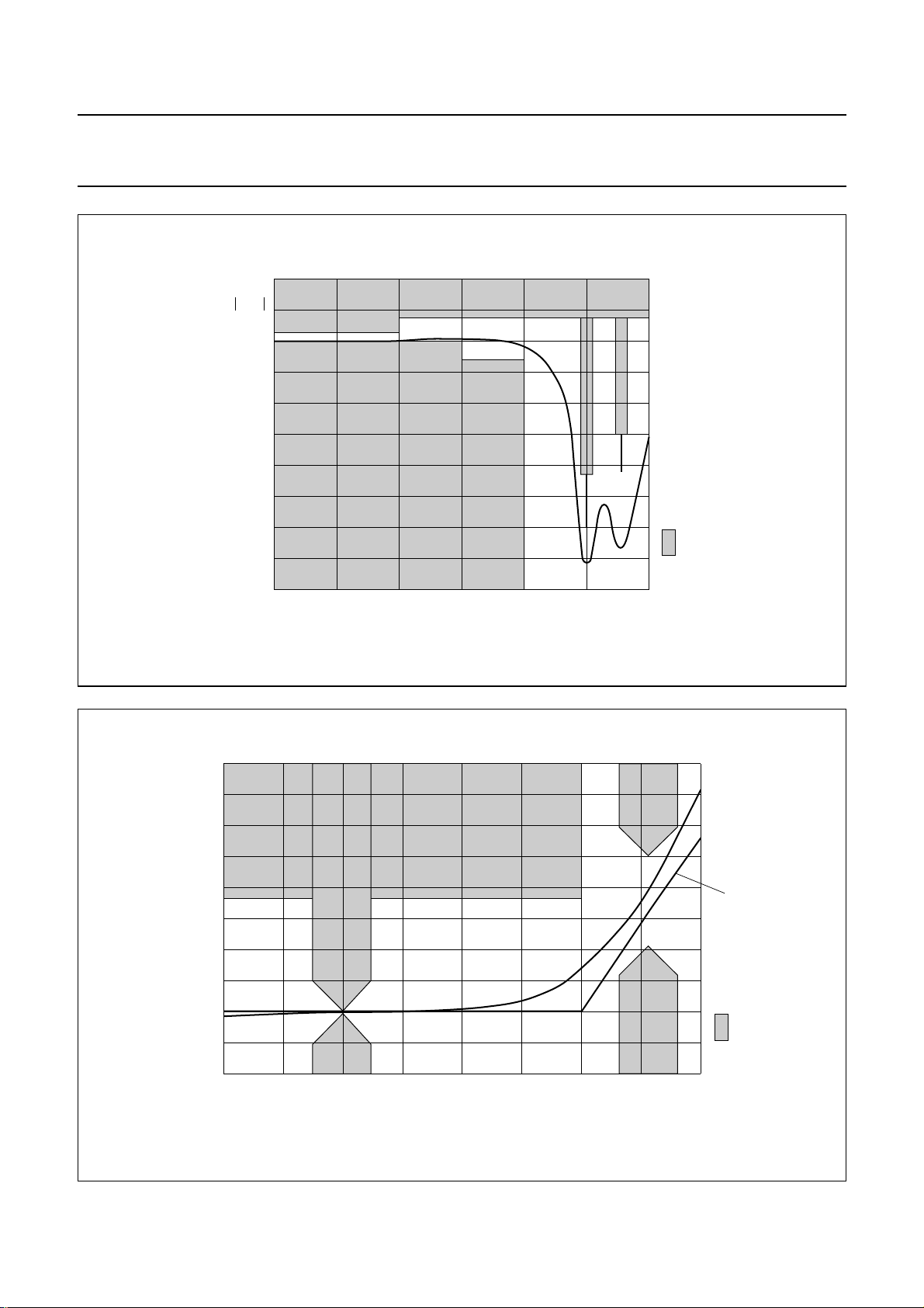
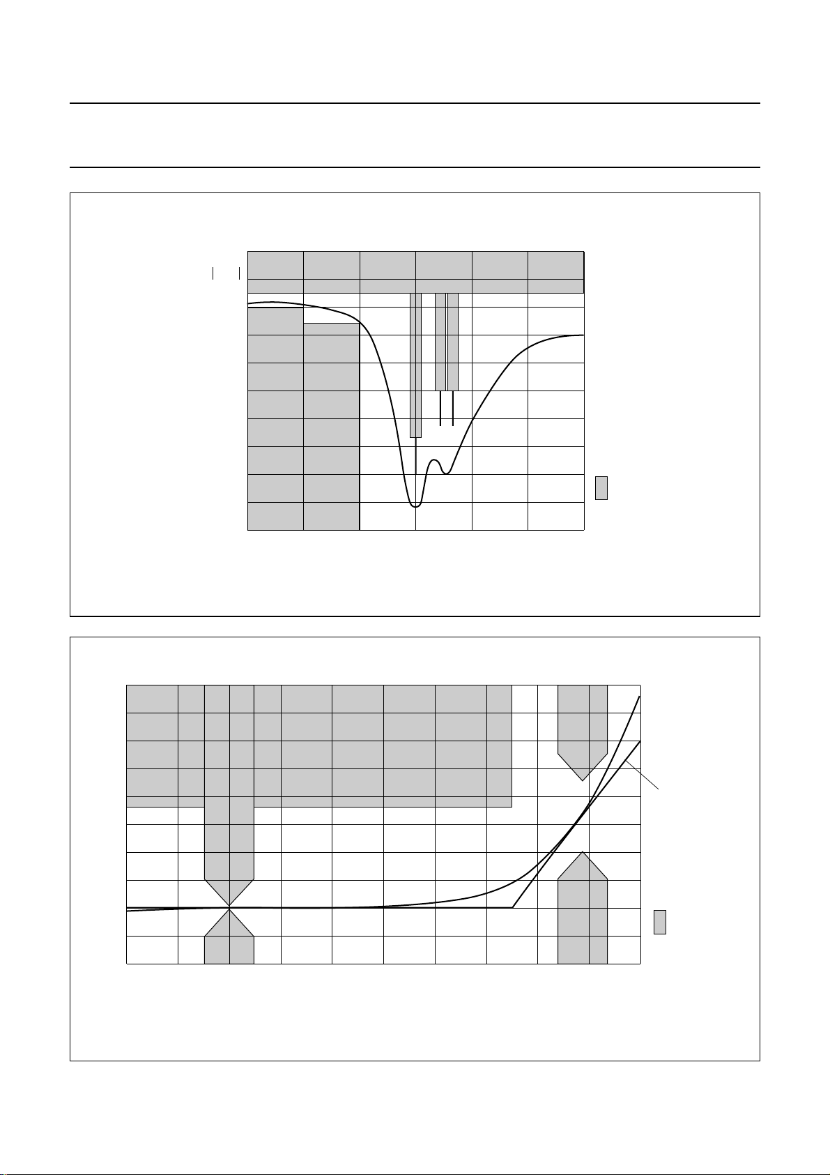
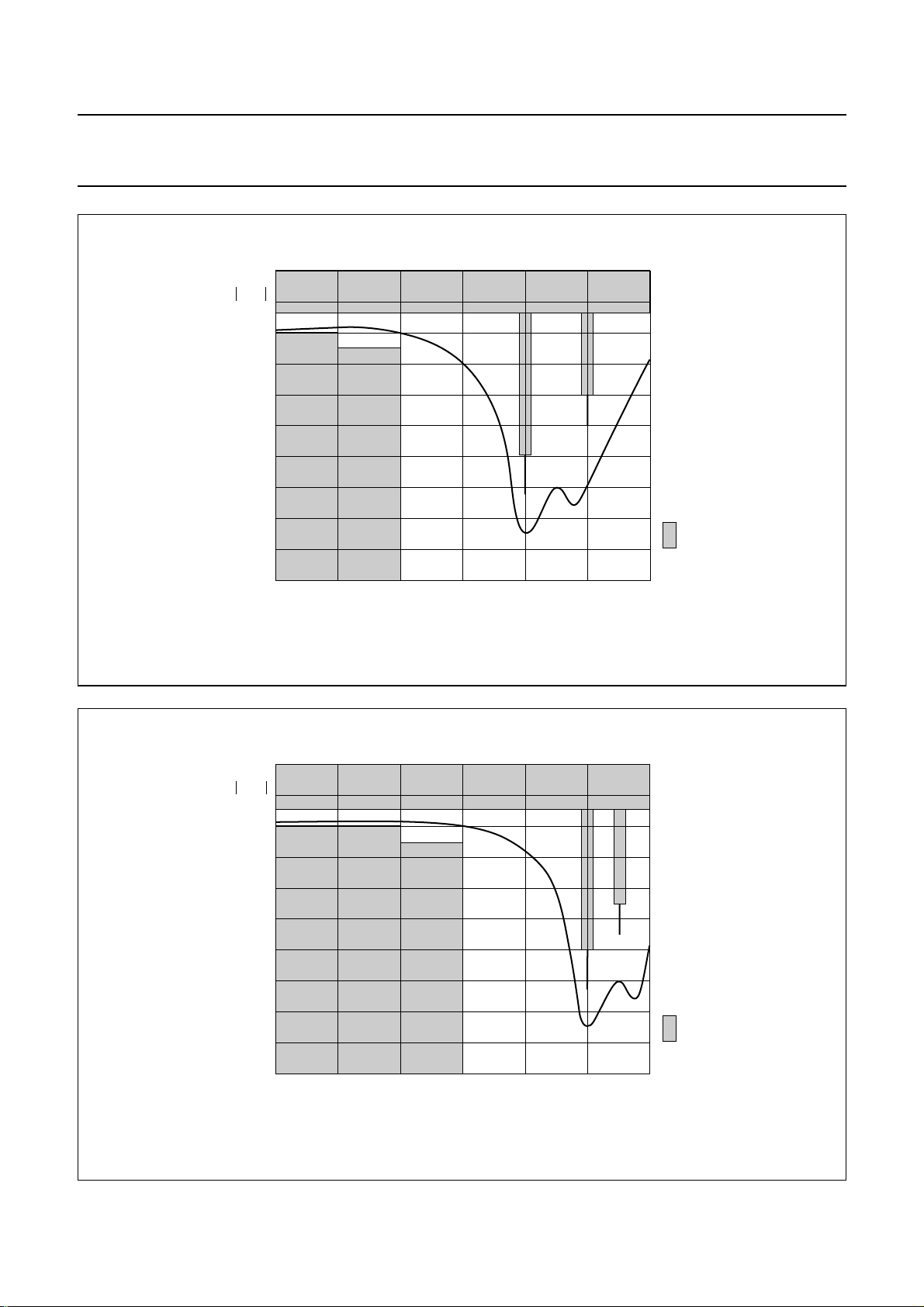
(see Figs 12 to 17); H (s) is the absolute value of transfer function.
9. S/N is the ratio of black-to-white amplitude to the black level noise voltage (RMS value, pin 13).
B = 4.2 MHz (M/N standard) or B = 5.0 MHz (B/G, I and D/K standard).
10. The intermodulation figures are defined:
αd
0.92
αd
2.76
20
20
---------------------------------------
V
at 0.92 MHz
0
at 3.58 MHz
V
0
log=
---------------------------------------
V
at 2.76 MHz
0
3.6 dB+log=
; αd
2.76
at 3.58 MHz
V
0
11. Measurements taken with SAW filter M1963M (sound shelf: 20 dB); loop bandwidth BL = 70 kHz.
a) Modulation Vestigial Side-Band (VSB); sound carrier off; f
b) Sound carrier on; f
= 10 kHz to 10 MHz.
video
12. The sound carrier trap can be disabled by switching pin 12 to ground (<0.8 V). In this way the full composite video
spectrum appears at pin 13. The amplitude is 1.1 V (p-p).
13. Response time valid for a VIF input level range of 200 µVto70mV.
operation as input
80 − 400 mV
terminal
−−4.7 kΩ
operation as input
22 100 − pF
terminal
µA
--------
rad
= loop bandwidth for −3 dB; d = damping factor.
−3dB
; αd
value at 0.92 MHz referenced to black or white signal;
0.92
value at 2.76 MHz referenced to chrominance carrier.
> 0.5 MHz.
video
2000 Nov 22 18
Page 19

Philips Semiconductors Product specification
Alignment-free multistandard vision and
TDA9880T
FM sound IF-PLL demodulator
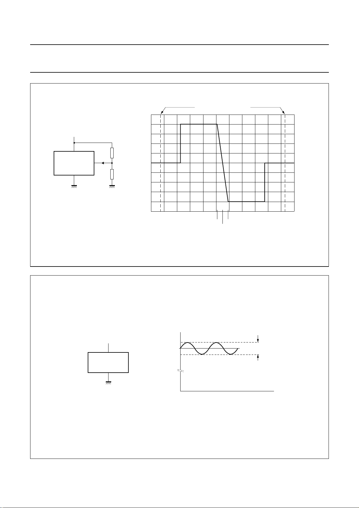
14. To match the AFC output signal to different tuning systems a current source output is provided. The test circuit is
given in Fig.7. The AFC steepness can be changed by resistors R1 and R2.
15. The tolerance of the reference frequencydeterminestheaccuracy of the VIF AFC, FM demodulatorcentrefrequency
and maximum FM deviation.
16. The intercarrier output signal at pin 11 can be calculated by the following formula taking into account the internal
video signal with 1.1 V (p-p) as a reference:
V
iSC()
dB()6 dB 3 dB±+
--------------V
iPC()
V
o(intc)(rms)
1.1 V (p-p)
1
× 10
---------- 22
where:
1
= correction term for RMS value, = sound-to-picture carrier ratio at VIF input(pins 1 and 2) in dB,
---------- 22
6 dB = correction term of internal circuitry and ±3 dB = tolerance of video output and intercarrier output amplitude
V
o(intc)(rms)
.
17. For normal operation no DC load at pin 11 is allowed, so the automatic audio mute function is not active.
By connecting a 2.2 kΩ resistor between pin 11 and ground the automatic audio mute function will be activated.
With this application also the series capacitor C
18. Calculation of the FM-PLL filter can be done approximately by use of the following formulae:
K
1
OKD
f
o
ϑ
=
---------------=
------ C
2π
-----------------------------------2R K
P
1
OKDCP
--------------------------------------------------------------- -
×=
V
iSC()
--------------V
iPC()
20
dB()
of the loop filter at pin 4 should be changed from 33 nF to 4.7 nF.
S
BL
fo1.55 ϑ2–()=
3 dB–
The formulae are only valid under the following conditions:
ϑ≤1 and C
>5C
S
P
where:
rad
K
= VCO steepness or ; KD= phase detector steepness ;
O
R
= loop resistor; CS= series capacitor; CP= parallel capacitor; fo= natural frequency of PLL;
S
BL
= loop bandwidth for −3 dB; ϑ = damping factor. For examples see Table 1.
−3dB
--------
V
Hz
2π
------ -
V
µA
--------
rad
19. For all S/N measurements the used vision IF modulator requires an incidental phase modulation for black-to-white
jump of less than 0.5 degrees.
20. Measurements taken with SAW filter M1963M (Siemens) for vision and sound IF (sound shelf: 20 dB).
Picture-to-sound carrier ratio of transmitter: PC/SC = 10 dB. Input level (at pins 1 and 2) V
i(VIF)(rms)
level), 25 kHz FM deviation for sound carrier, fAF= 400 Hz. Measurement in accordance with
= 10 mV (sync
“CCIR 468-4”
.
De-emphasis = 75 µs.
21. The PC/SC ratio is calculated as the addition of TV transmitter PC/SC ratio and SAW filter PC/SC ratio. This PC/SC
ratio is necessary to achieve the S/NW values as noted. A different PC/SC ratio will change these values.
22. Measured with an FM deviation of 25 kHz, the typical AF output signal is 500 mV (RMS). By using Rx=20kΩ the
AF output signal is attenuated by 6 dB, so 250 mV (RMS). For handling an FM deviation of more than 55 kHz the
AF output signal has to be reduced by using Rx in order to avoid clipping (THD < 1.5%). For an FM deviation up to
100 kHz an attenuation of 6 dB is recommended.
23. C
= 10 nF results in τ =50µs and C
DEEM
= 15 nF results in τ =75µs.
DEEM
2000 Nov 22 19
Page 20

Philips Semiconductors Product specification
Alignment-free multistandard vision and
TDA9880T
FM sound IF-PLL demodulator
24. The lower limit of audio bandwidth depends on the value of the capacitor at pin 6. A value of C
f
AF(−3 dB)
≈ 20 Hz and C
= 220 nF leads to f
AFD
AF(−3 dB)
≈ 40 Hz.
25. The reference input pin 15 is able to operate as a 1-pin crystal oscillator as well as an input terminal with external
reference signal, e.g. from the tuning system.
26. The value of Cxdetermines the accuracy of the resonance frequency of the crystal. It depends on the type of crystal
used.
Table 1 Examples to note 18 of Chapter “Characteristics”
BL
(kHz) CS (nF) CP (pF) R (kΩ) ϑ
−3dB
100 33 820 2.7 0.5
160 33 330 3.9 0.5
Table 2 Standard switch settings
S0 S1 f
(MHz) f
VIF
(MHz) STANDARD REMARK
intc
LOW LOW 38.9 5.5 B/G Europe
LOW MID 38.9 6.5 D/K
LOW HIGH 38.9 6.0 I United Kingdom
MID LOW 38.0 5.5 B/G
MID MID 38.0 6.0 I
MID HIGH 38.0 6.5 D/K
HIGH LOW 45.75 4.5 M/N USA
HIGH MID 38.0 4.5 M
HIGH HIGH 58.75 4.5 M Japan
= 470 nF leads to
AFD
2000 Nov 22 20
Page 21
Philips Semiconductors Product specification
Alignment-free multistandard vision and
FM sound IF-PLL demodulator
handbook, halfpage
V
20
(V)
4
3
2
1
30 50 110
(2) (3) (4)(1)
70 90
V
i(VIF)
MHB158
(dB/µV)
(µA)
600
500
400
300
200
100
0
I
14
120
handbook, halfpage
V
i(VIF)
(dBµV)
100
90
80
70
60
024
TDA9880T
MHB159
12820416
R
TOP
(kΩ)
(1) VIF AGC voltage.
(2) I
; R
TOP
=22kΩ.
tuner
(3) I
(4) I
tuner
tuner
; R
; R
TOP
TOP
=12kΩ.
=0Ω.
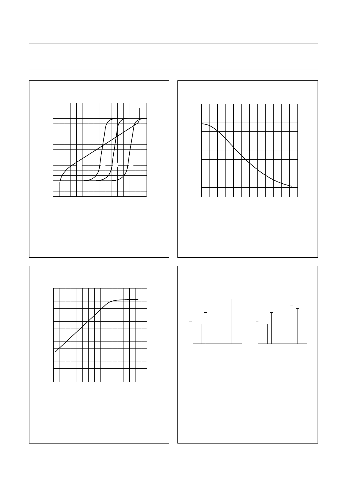
Fig.3 Typical VIF and tuner AGC characteristic.
70
handbook, halfpage
S/N
(dB)
60
50
40
30
20
10
0
30 50 110
70 90
V
i(VIF)
MHB160
(dB/µV)
Fig.5 Typical signal-to-noise ratio as a function of
VIF input voltage.
Fig.4 Typical tuner takeoverpoint as a function of
R
.
TOP
handbook, halfpage
13.2 dB
21 dB
SC CC PC SC CC PC
3.2 dB
13.2 dB
21 dB
BLUE YELLOW
SC = sound carrier, with respect to sync level.
CC = chrominance carrier, with respect to sync level.
PC = picture carrier, with respect to sync level.
The sound carrier levels are taking into account a sound shelf
attenuation of 20 dB (SAW filter M1963M).
Fig.6 Input signal conditions.
10 dB
MHA739
2000 Nov 22 21
Page 22
Philips Semiconductors Product specification
Alignment-free multistandard vision and
FM sound IF-PLL demodulator
handbook, full pagewidth
5
V
19
V
P
TDA9880T
R1
22 kΩ
I
19
19
R2
22 kΩ
MHB075
(V)
4
3
2
1
0
43 48
lock range without SAW filter
44 45 46
45.75
45.94
45.56
47
f (MHz)
TDA9880T
−200
I
19
(µA)
−100
0
100
200
handbook, full pagewidth
Fig.7 Measurement conditions and typical AFC characteristic.
VP = 5 V
VP = 5 V
TDA9880T
MHB076
(f
ripple
100 mV
= 70 Hz)
t
Fig.8 Ripple rejection condition.
2000 Nov 22 22
Page 23
Philips Semiconductors Product specification
Alignment-free multistandard vision and
FM sound IF-PLL demodulator
handbook, full pagewidth
2.6 V
1.5 V
3.57 V
3.35 V
1.95 V
1.35 V
2.72 V
1.83 V
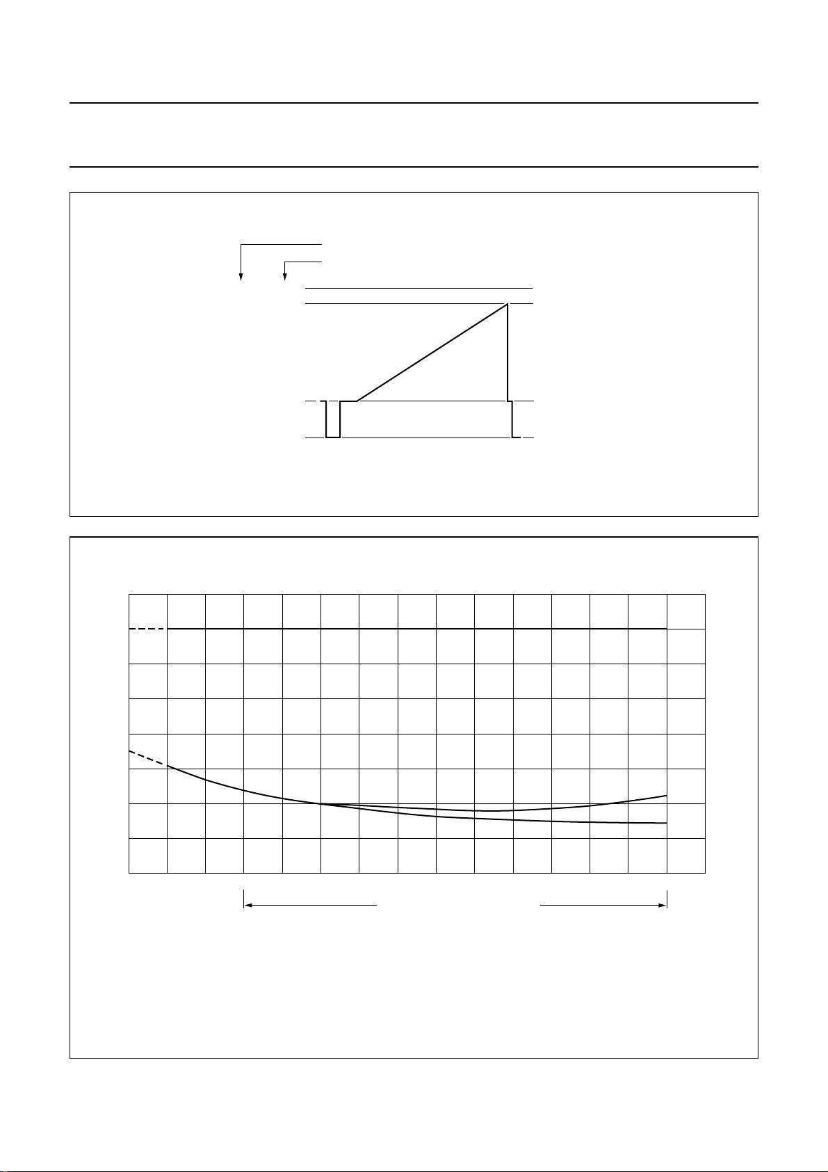
Fig.9 Typical video signal levels on output pin 13 (sound carrier off).
trap bypass mode
normal mode
TDA9880T
zero carrier level
white level
black level
sync level
MHB163
10
handbook, full pagewidth
audio
0
S/N
(dB)
−10
−20
−30
−40
−50
−60
−70
49 46 43 40 1337 10 728 2225 193134 16
Conditions: 25 kHz FM deviation; 75 µs de-emphasis.
(1) Signal.
(2) Noise at H-picture.
(3) Noise at black picture.
MHB164
(1)
(2)
(3)
4
gain controlled operation of FM-PLL
PC/SC ratio at pins 1 and 2 (dB)
Fig.0 Audio S/N as a function of picture-to-sound carrier ratio.
2000 Nov 22 23
Page 24
Philips Semiconductors Product specification
Alignment-free multistandard vision and
FM sound IF-PLL demodulator
(dBµV)
120
100
(1)
80
tuner gain
control range
handbook, full pagewidth
antenna input
SAW insertion
loss 14 dB
IF slip
6 dB
70 dB
VIF AGC
MHB079
TDA9880T
1
video 1.1 V (p-p)
−1
10
IF signals
RMS value
(V)
−2
10
(TOP)
−3
60
SAW insertion
loss 14 dB
40
40 dB
RF gain
20
10
VHF/UHF tuner VIF
tuner SAW filter
VIF amplifier, demodulator
and video
TDA9880T
10
0.66 × 10
−4
10
−5
10
0.66 × 10
−3
−5
(1) Depends on TOP.
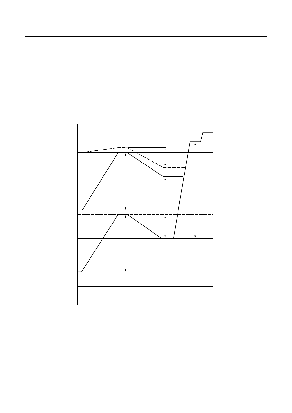
Fig.11 Front-end level diagram.
2000 Nov 22 24
Page 25
Philips Semiconductors Product specification
Alignment-free multistandard vision and
FM sound IF-PLL demodulator
handbook, full pagewidth
10
H (s)
(dB)
0
−10
−20
−30
−40
2 2.5 3 3.5 4 4.5 5
TDA9880T
MHB166
minimum
requirements
f (MHz)
handbook, full pagewidth
Fig.12 Typical amplitude response for sound trap at M/N standard (including Korea).
400
group
delay
(ns)
300
200
100
0
−100
0 0.5 1.5 2 31 2.5 3.5 4
MHB167
due to pre-correction
f (MHz)
ideal characteristic
in the transmitter
minimum
requirements
Remark: overall delay is not shown, here the maximum ripple is specified.
Fig.13 Typical group delay for sound trap at M/N standard.
2000 Nov 22 25
Page 26
Philips Semiconductors Product specification
Alignment-free multistandard vision and
FM sound IF-PLL demodulator
handbook, full pagewidth
10
H (s)
(dB)
0
−10
−20
−30
−40
4 4.5 5 5.5 6 6.5 7
TDA9880T
MHB168
minimum
requirements
f (MHz)
400
handbook, full pagewidth
group
delay
(ns)
300
200
100
0
−100
0 0.5 1.5 2 31 2.5 3.5 4 4.5 5
Fig.14 Typical amplitude response for sound trap at B/G standard.
MHB169
ideal characteristic
due to pre-correction
in the transmitter
minimum
requirements
f (MHz)
Remark: Overall delay is not shown, here the maximum ripple is specified.
Fig.15 Typical group delay for sound trap at B/G standard.
2000 Nov 22 26
Page 27
Philips Semiconductors Product specification
Alignment-free multistandard vision and
FM sound IF-PLL demodulator
handbook, full pagewidth
10
H (s)
(dB)
0
−10
−20
−30
−40
4 4.5 5 5.5 6 6.5 7
TDA9880T
MHB170
minimum
requirements
f (MHz)
handbook, full pagewidth
Fig.16 Typical amplitude response for sound trap at I standard.
10
H (s)
(dB)
0
−10
−20
−30
−40
4 4.5 5 5.5 6 6.5 7
MHB171
f (MHz)
minimum
requirements
Fig.17 Typical amplitude response for sound trap at D/K standard.
2000 Nov 22 27
Page 28
This text is here in white to force landscape pages to be rotated correctly when browsing through the pdf in the Acrobat reader.This text is here in
_white to force landscape pages to be rotated correctly when browsing through the pdf in the Acrobat reader.This text is here inThis text is here in
white to force landscape pages to be rotated correctly when browsing through the pdf in the Acrobat reader. white to force landscape pages to be ...
2000 Nov 22 28
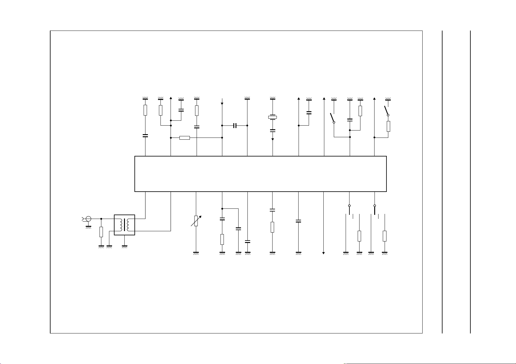
TEST CIRCUIT
Alignment-free multistandard vision and
FM sound IF-PLL demodulator
Philips Semiconductors Product specification
IF
input
AFC
output
1.5
22
kΩ
kΩ
C
VAGC
10 nF
VAGC AFC VPLL
20
22 kΩ
(1)
VIF-PLL
filter
100
R
nF
150 Ω
1819 1417 16 15
C
220 nF
V
P
10 nF
V
P
GND REF
4 MHz
(3)
C
x
f
ref
TAGC
output
CVBS
output
10
nF
TAGC CVBS TR SIO
C
TR
470
nF
bypass
13 12 11
sound
intercarrier
output
3.3
MΩ
auto
mute
2.2
kΩ
TDA9880T
13 72456
VIF1 VIF2 TOP FMPLL
1
: 1
22 kΩ
50
Ω
R
TOP
C
33 nF
R
2.7 kΩ
S
S
FM-PLL
filter
(2)
C
820
pF
P
DEEM AFD FAGC AUD S0 S1
470 nF
C
100 nF
C
DEEM
15 nF
(4)
R
x
8910
FAGC
output
LM
H
logicaudio
LM
H
47
kΩ
47
kΩ
MHB162
(1) See note 4 of Chapter “Characteristics”.
(2) See notes 17 and 18 of Chapter “Characteristics”.
(3) See note 26 of Chapter “Characteristics”.
(4) See note 22 of Chapter “Characteristics”.
Fig.18 Test circuit.
TDA9880T
handbook, full pagewidth
Page 29
Philips Semiconductors Product specification
Alignment-free multistandard vision and
FM sound IF-PLL demodulator
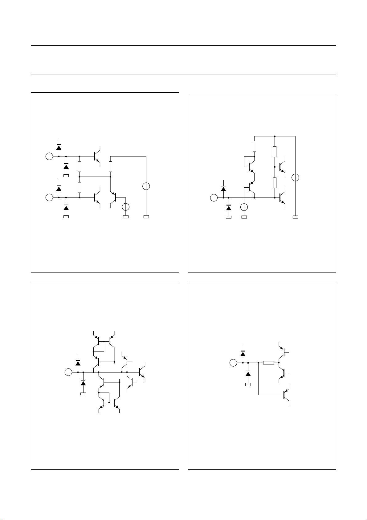
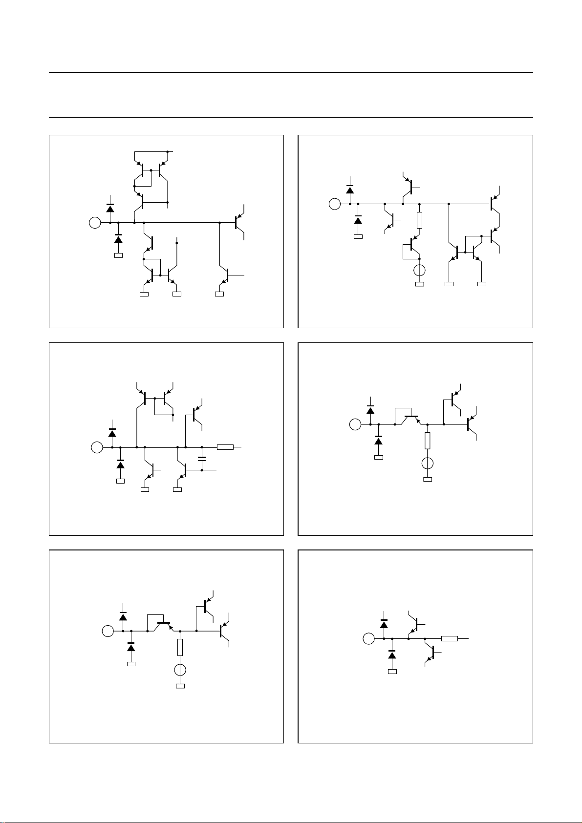
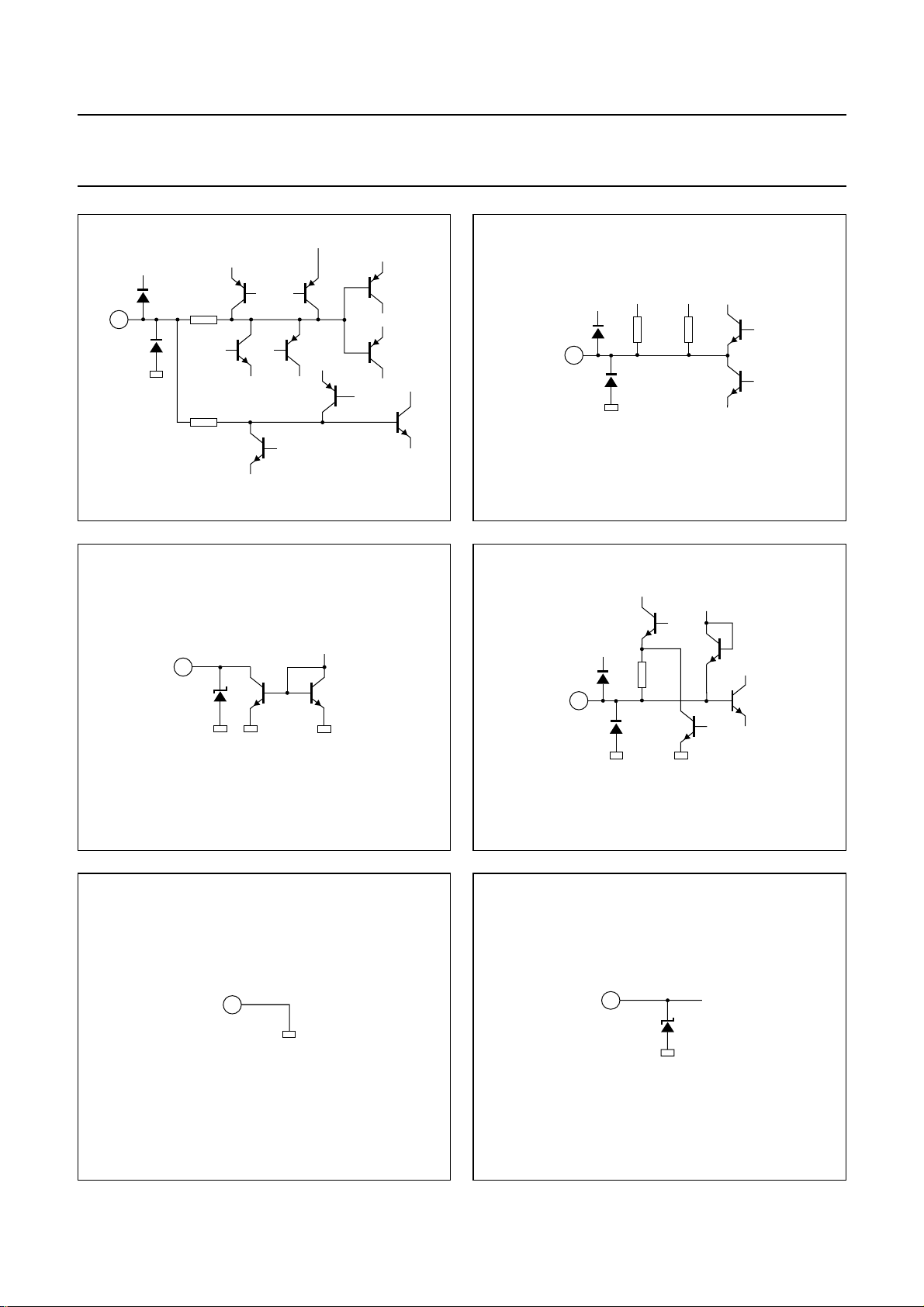
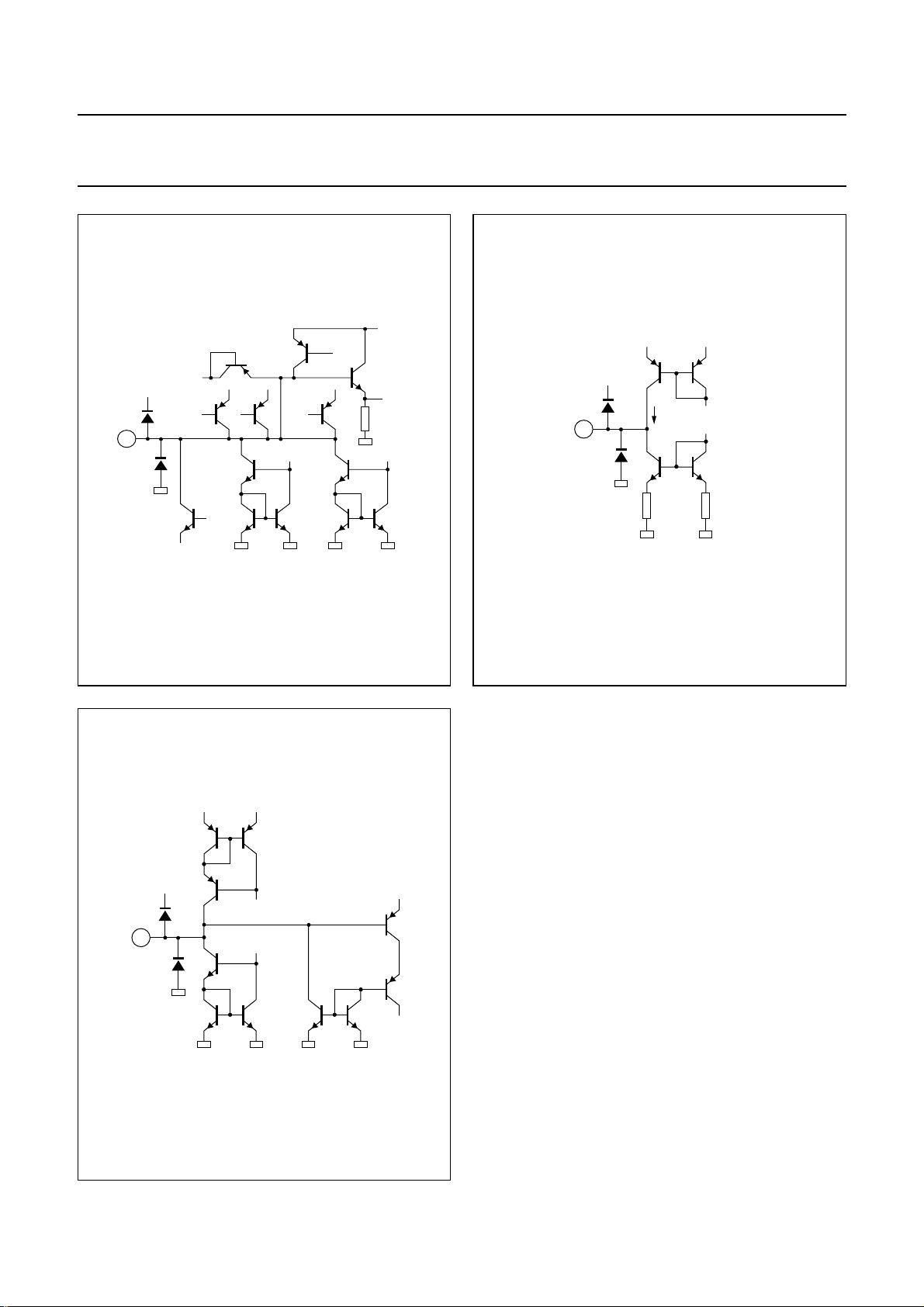
INTERNAL PIN CONFIGURATIONS
handbook, halfpage
+
1
1.1 kΩ 5 kΩ
+
1.1 kΩ
2
2.65 V
3.55 V
MHB087
handbook, halfpage
3
TDA9880T
30 kΩ
+
1.9 V
20 kΩ
3.55 V
9 kΩ
MHB088
Fig.19 Pin 1 (VIF1) and pin 2 (VIF2).
handbook, halfpage
maximum 100 µA
+
4
maximum 100 µA
MHB089
andbook, halfpage
Fig.20 Pin 3 (TOP).
+
5
240 µA
5.0 kΩ
MHB090
Fig.21 Pin 4 (FMPLL).
2000 Nov 22 29
Fig.22 Pin 5 (DEEM).
Page 30
Philips Semiconductors Product specification
Alignment-free multistandard vision and
FM sound IF-PLL demodulator
handbook, halfpage
+
6
Fig.23 Pin 6 (AFD).
+
maximum 1.5 µA
maximum 1.5 µA
MHB091
handbook, halfpage
7
maximum 2.2 µA
+
maximum
2.2 µA
Fig.24 Pin 7 (FAGC).
TDA9880T
2 kΩ
1.5 V
MHB092
handbook, halfpage
8
handbook, halfpage
++
+
Fig.25 Pin 8 (AUD).
+
10
600 µA
27 kΩ
15 kΩ
10 pF
MHB093
handbook, halfpage
handbook, halfpage
+
9
Fig.26 Pin 9 (S0).
+
11
27 kΩ
3.55 V
MHB094
14.7 kΩ
3.55 V
MHB095
Fig.27 Pin 10 (S1).
2000 Nov 22 30
1.2 mA
MHB096
Fig.28 Pin 11 (SIO).
Page 31
Philips Semiconductors Product specification
Alignment-free multistandard vision and
FM sound IF-PLL demodulator
handbook, halfpage
+
12
maximum 9 µA
1 kΩ
maximum 13 µA
500 Ω
Fig.29 Pin 12 (TR).
maximum 150 µA
1.1 V
MHB165
handbook, halfpage
+
13
MHB098
Fig.30 Pin 13 (CVBS).
TDA9880T
+
7 kΩ10 kΩ
2.5 mA
handbook, halfpage
handbook, halfpage
14
maximum
600 µA
Fig.31 Pin 14 (TAGC).
16GND
MHB101
MHB099
handbook, halfpage
handbook, halfpage
+
3 kΩ
15
200 µA
Fig.32 Pin 15 (REF).
17
MHB100
+
MHB102
Fig.33 Pin 16 (GND).
2000 Nov 22 31
Fig.34 Pin 17 (VP).
Page 32
Philips Semiconductors Product specification
Alignment-free multistandard vision and
FM sound IF-PLL demodulator
handbook, halfpage
+
18
maximum
15 µA
maximum
5 µA
+
VCO
25 kΩ
MHB103
handbook, halfpage
TDA9880T
+
19
maximum 200 µA
1 kΩ
1 kΩ
MHB104
handbook, halfpage
20
Fig.35 Pin 18 (VPLL).
+
maximum 8 µA
maximum 10 µA
Fig.36 Pin 19 (AFC).
MHB105
Fig.37 Pin 20 (VAGC).
2000 Nov 22 32
Page 33
Philips Semiconductors Product specification
Alignment-free multistandard vision and
FM sound IF-PLL demodulator
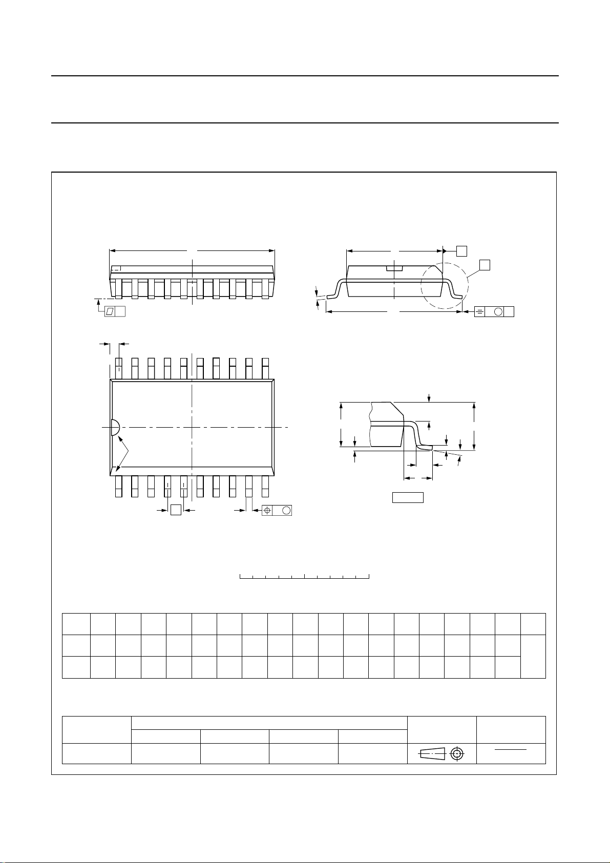
PACKAGE OUTLINE
SO20: plastic small outline package; 20 leads; body width 7.5 mm
D
c
y
Z
20
11
TDA9880T
SOT163-1
E
H
E
A
X
v M
A
pin 1 index
1
e
0 5 10 mm
DIMENSIONS (inch dimensions are derived from the original mm dimensions)
mm
A
max.
2.65
0.10
A
0.30
0.10
0.012
0.004
1
A2A
2.45
2.25
0.096
0.089
0.25
0.01
b
0.49
0.36
p
cD
0.32
0.23
0.013
0.009
3
0.019
0.014
UNIT
inches
Note
1. Plastic or metal protrusions of 0.15 mm maximum per side are not included.
10
w M
b
p
scale
(1)E(1) (1)
13.0
12.6
0.51
0.49
eHELLpQ
7.6
1.27
7.4
0.30
0.050
0.29
10.65
10.00
0.419
0.394
Q
A
2
0.055
A
1.4
1
detail X
1.1
1.1
1.0
0.4
0.043
0.043
0.039
0.016
(A )
L
p
L
0.25
0.01
A
3
θ
0.25 0.1
0.01
ywv θ
Z
0.9
0.4
8
0.004
0.035
0.016
0
o
o
OUTLINE
VERSION
SOT163-1
IEC JEDEC EIAJ
075E04 MS-013
REFERENCES
2000 Nov 22 33
EUROPEAN
PROJECTION
ISSUE DATE
97-05-22
99-12-27
Page 34

Philips Semiconductors Product specification
Alignment-free multistandard vision and
FM sound IF-PLL demodulator
SOLDERING
Introduction to soldering surface mount packages
Thistextgivesa very brief insight to a complex technology.
A more in-depth account of soldering ICs can be found in
our
“Data Handbook IC26; Integrated Circuit Packages”
(document order number 9398 652 90011).
There is no soldering method that is ideal for all surface
mount IC packages. Wave soldering can still be used for
certainsurfacemountICs,butit is not suitable for fine pitch
SMDs. In these situations reflow soldering is
recommended.
Reflow soldering
Reflow soldering requires solder paste (a suspension of
fine solder particles, flux and binding agent) to be applied
tothe printed-circuit board by screen printing,stencillingor
pressure-syringe dispensing before package placement.
Several methods exist for reflowing; for example,
convection or convection/infrared heating in a conveyor
type oven. Throughput times (preheating, soldering and
cooling) vary between 100 and 200 seconds depending
on heating method.
Typical reflow peak temperatures range from
215 to 250 °C. The top-surface temperature of the
packages should preferable be kept below 220 °C for
thick/large packages, and below 235 °C for small/thin
packages.
Wave soldering
Conventional single wave soldering is not recommended
forsurfacemountdevices(SMDs)or printed-circuit boards
with a high component density, as solder bridging and
non-wetting can present major problems.
To overcome these problems the double-wave soldering
method was specifically developed.
TDA9880T
If wave soldering is used the following conditions must be
observed for optimal results:
• Use a double-wave soldering method comprising a
turbulent wave with high upward pressure followed by a
smooth laminar wave.
• For packages with leads on two sides and a pitch (e):
– larger than or equal to 1.27 mm, the footprint
longitudinal axis is preferred to be parallel to the
transport direction of the printed-circuit board;
– smaller than 1.27 mm, the footprint longitudinal axis
must be parallel to the transport direction of the
printed-circuit board.
The footprint must incorporate solder thieves at the
downstream end.
• Forpackageswithleadsonfoursides,thefootprintmust
be placed at a 45° angle to the transport direction of the
printed-circuit board. The footprint must incorporate
solder thieves downstream and at the side corners.
During placement and before soldering, the package must
be fixed with a droplet of adhesive. The adhesive can be
applied by screen printing, pin transfer or syringe
dispensing. The package can be soldered after the
adhesive is cured.
Typical dwell time is 4 seconds at 250 °C.
A mildly-activated flux will eliminate the need for removal
of corrosive residues in most applications.
Manual soldering
Fix the component by first soldering two
diagonally-opposite end leads. Use a low voltage (24 V or
less) soldering iron applied to the flat part of the lead.
Contact time must be limited to 10 seconds at up to
300 °C.
When using a dedicated tool, all other leads can be
soldered in one operation within 2 to 5 seconds between
270 and 320 °C.
2000 Nov 22 34
Page 35

Philips Semiconductors Product specification
Alignment-free multistandard vision and
TDA9880T
FM sound IF-PLL demodulator
Suitability of surface mount IC packages for wave and reflow soldering methods
PACKAGE
BGA, LFBGA, SQFP, TFBGA not suitable suitable
HBCC, HLQFP, HSQFP, HSOP, HTQFP, HTSSOP, SMS not suitable
(3)
PLCC
LQFP, QFP, TQFP not recommended
SSOP, TSSOP, VSO not recommended
Notes
1. All surface mount (SMD) packages are moisture sensitive. Depending upon the moisture content, the maximum
2. These packages are not suitable for wave soldering as a solder joint between the printed-circuit board and heatsink
3. If wave soldering is considered, then the package must be placed at a 45° angle to the solder wave direction.
4. Wave soldering is only suitable for LQFP, TQFP and QFP packages with a pitch (e) equal to or larger than 0.8 mm;
5. Wave soldering is only suitable for SSOP and TSSOP packages with a pitch (e) equal to or larger than 0.65 mm; it is
, SO, SOJ suitable suitable
temperature (with respect to time) and body size of the package, there is a risk that internal or external package
cracks may occur due to vaporization of the moisture in them (the so called popcorn effect). For details, refer to the
Drypack information in the
(at bottom version) can not be achieved, and as solder may stick to the heatsink (on top version).
The package footprint must incorporate solder thieves downstream and at the side corners.
it is definitely not suitable for packages with a pitch (e) equal to or smaller than 0.65 mm.
definitely not suitable for packages with a pitch (e) equal to or smaller than 0.5 mm.
“Data Handbook IC26; Integrated Circuit Packages; Section: Packing Methods”
SOLDERING METHOD
WAVE REFLOW
(2)
(3)(4)
(5)
suitable
suitable
suitable
(1)
.
2000 Nov 22 35
Page 36

Philips Semiconductors Product specification
Alignment-free multistandard vision and
TDA9880T
FM sound IF-PLL demodulator
DATA SHEET STATUS
DATA SHEET STATUS
Objective specification Development This data sheet contains the design target or goal specifications for
Preliminary specification Qualification This data sheet contains preliminary data, and supplementary data will be
Product specification Production This data sheet contains final specifications. Philips Semiconductors
Note
1. Please consult the most recently issued data sheet before initiating or completing a design.
DEFINITIONS
Short-form specification The data in a short-form
specification is extracted from a full data sheet with the
same type number and title. For detailed information see
the relevant data sheet or data handbook.
Limiting values definition Limiting values given are in
accordance with the Absolute Maximum Rating System
(IEC 60134). Stress above one or more of the limiting
values may cause permanent damage to the device.
These are stress ratings only and operation of the device
attheseor at any other conditions above those giveninthe
Characteristics sections of the specification is not implied.
Exposure to limiting values for extended periods may
affect device reliability.
Application information Applications that are
described herein for any of these products are for
illustrative purposes only. Philips Semiconductors make
norepresentationorwarrantythatsuchapplicationswillbe
suitable for the specified use without further testing or
modification.
PRODUCT
STATUS
DEFINITIONS
product development. Specification may change in any manner without
notice.
published at a later date. Philips Semiconductors reserves the right to
make changes at any time without notice in order to improve design and
supply the best possible product.
reserves the right to make changes at any time without notice in order to
improve design and supply the best possible product.
DISCLAIMERS
Life support applications These products are not
designed for use in life support appliances, devices, or
systems where malfunction of these products can
reasonably be expected toresult in personal injury. Philips
Semiconductorscustomersusingorsellingtheseproducts
for use in such applications do so at their own risk and
agree to fully indemnify Philips Semiconductors for any
damages resulting from such application.
Right to make changes Philips Semiconductors
reserves the right to make changes, without notice, in the
products, including circuits, standard cells, and/or
software, described or contained herein in order to
improve design and/or performance. Philips
Semiconductors assumes no responsibility or liability for
theuseofanyofthese products, conveys no licence or title
under any patent, copyright, or mask work right to these
products,andmakes no representations or warranties that
these products are free from patent, copyright, or mask
work right infringement, unless otherwise specified.
(1)
2000 Nov 22 36
Page 37

Philips Semiconductors Product specification
Alignment-free multistandard vision and
FM sound IF-PLL demodulator
NOTES
TDA9880T
2000 Nov 22 37
Page 38

Philips Semiconductors Product specification
Alignment-free multistandard vision and
FM sound IF-PLL demodulator
NOTES
TDA9880T
2000 Nov 22 38
Page 39

Philips Semiconductors Product specification
Alignment-free multistandard vision and
FM sound IF-PLL demodulator
NOTES
TDA9880T
2000 Nov 22 39
Page 40

Philips Semiconductors – a w orldwide compan y
Argentina: see South America
Australia: 3 Figtree Drive, HOMEBUSH, NSW 2140,
Tel. +61 2 9704 8141, Fax. +61 2 9704 8139
Austria: Computerstr. 6, A-1101 WIEN, P.O. Box 213,
Tel. +43 1 60 101 1248, Fax. +43 1 60 101 1210
Belarus: Hotel Minsk Business Center, Bld. 3, r. 1211, Volodarski Str. 6,
220050 MINSK, Tel. +375 172 20 0733, Fax. +375 172 20 0773
Belgium: see The Netherlands
Brazil: see South America
Bulgaria: Philips Bulgaria Ltd., Energoproject, 15th floor,
51 James Bourchier Blvd., 1407 SOFIA,
Tel. +359 2 68 9211, Fax. +359 2 68 9102
Canada: PHILIPS SEMICONDUCTORS/COMPONENTS,
Tel. +1 800 234 7381, Fax. +1 800 943 0087
China/Hong Kong: 501 Hong Kong Industrial Technology Centre,
72 Tat Chee Avenue, Kowloon Tong, HONG KONG,
Tel. +852 2319 7888, Fax. +852 2319 7700
Colombia: see South America
Czech Republic: see Austria
Denmark: Sydhavnsgade 23, 1780 COPENHAGEN V,
Tel. +45 33 29 3333, Fax. +45 33 29 3905
Finland: Sinikalliontie 3, FIN-02630 ESPOO,
Tel. +358 9 615 800, Fax. +358 9 6158 0920
France: 51 Rue Carnot, BP317, 92156 SURESNES Cedex,
Tel. +33 1 4099 6161, Fax. +33 1 4099 6427
Germany: Hammerbrookstraße 69, D-20097 HAMBURG,
Tel. +49 40 2353 60, Fax. +49 40 2353 6300
Hungary: see Austria
India: Philips INDIA Ltd, Band Box Building, 2nd floor,
254-D, Dr. Annie Besant Road, Worli, MUMBAI 400 025,
Tel. +91 22 493 8541, Fax. +91 22 493 0966
Indonesia: PT Philips DevelopmentCorporation, SemiconductorsDivision,
Gedung Philips, Jl. Buncit Raya Kav.99-100, JAKARTA 12510,
Tel. +62 21 794 0040 ext. 2501, Fax. +62 21 794 0080
Ireland: Newstead, Clonskeagh, DUBLIN 14,
Tel. +353 1 7640 000, Fax. +353 1 7640 200
Israel: RAPAC Electronics, 7 Kehilat Saloniki St, PO Box 18053,
TEL AVIV 61180, Tel. +972 3 645 0444, Fax. +972 3 649 1007
Italy: PHILIPS SEMICONDUCTORS, Via Casati, 23 - 20052 MONZA (MI),
Tel. +39 039 203 6838, Fax +39 039 203 6800
Japan: Philips Bldg 13-37, Kohnan 2-chome, Minato-ku,
TOKYO 108-8507, Tel. +81 3 3740 5130, Fax. +81 3 3740 5057
Korea: Philips House, 260-199 Itaewon-dong, Yongsan-ku, SEOUL,
Tel. +82 2 709 1412, Fax. +82 2 709 1415
Malaysia: No. 76 Jalan Universiti, 46200 PETALING JAYA, SELANGOR,
Tel. +60 3 750 5214, Fax. +60 3 757 4880
Mexico: 5900 Gateway East, Suite 200, EL PASO, TEXAS 79905,
Tel. +9-5 800 234 7381, Fax +9-5 800 943 0087
Middle East: see Italy
Netherlands: Postbus 90050, 5600 PB EINDHOVEN, Bldg. VB,
Tel. +31 40 27 82785, Fax. +31 40 27 88399
New Zealand: 2 Wagener Place, C.P.O. Box 1041, AUCKLAND,
Tel. +64 9 849 4160, Fax. +64 9 849 7811
Norway: Box 1, Manglerud 0612, OSLO,
Tel. +47 22 74 8000, Fax. +47 22 74 8341
Pakistan: see Singapore
Philippines: Philips Semiconductors Philippines Inc.,
106 Valero St. Salcedo Village, P.O. Box 2108 MCC, MAKATI,
Metro MANILA, Tel. +63 2 816 6380, Fax. +63 2 817 3474
Poland: Al.Jerozolimskie 195 B, 02-222 WARSAW,
Tel. +48 22 5710 000, Fax. +48 22 5710 001
Portugal: see Spain
Romania: see Italy
Russia: Philips Russia, Ul. Usatcheva 35A, 119048 MOSCOW,
Tel. +7 095 755 6918, Fax. +7 095 755 6919
Singapore: Lorong 1, Toa Payoh, SINGAPORE 319762,
Tel. +65 350 2538, Fax. +65 251 6500
Slovakia: see Austria
Slovenia: see Italy
South Africa: S.A. PHILIPS Pty Ltd., 195-215 Main Road Martindale,
2092 JOHANNESBURG, P.O. Box 58088 Newville 2114,
Tel. +27 11 471 5401, Fax. +27 11 471 5398
South America: Al. Vicente Pinzon, 173, 6th floor,
04547-130 SÃO PAULO, SP, Brazil,
Tel. +55 11 821 2333, Fax. +55 11 821 2382
Spain: Balmes 22, 08007 BARCELONA,
Tel. +34 93 301 6312, Fax. +34 93 301 4107
Sweden: Kottbygatan 7, Akalla, S-16485 STOCKHOLM,
Tel. +46 8 5985 2000, Fax. +46 8 5985 2745
Switzerland: Allmendstrasse 140, CH-8027 ZÜRICH,
Tel. +41 1 488 2741 Fax. +41 1 488 3263
Taiwan: Philips Semiconductors, 5F, No. 96, Chien Kuo N. Rd., Sec. 1,
TAIPEI, Taiwan Tel. +886 2 2134 2451, Fax. +886 2 2134 2874
Thailand: PHILIPS ELECTRONICS (THAILAND) Ltd.,
60/14 MOO 11, Bangna Trad Road KM. 3, Bagna, BANGKOK 10260,
Tel. +66 2 361 7910, Fax. +66 2 398 3447
Turkey: Yukari Dudullu, Org. San. Blg., 2.Cad. Nr. 28 81260 Umraniye,
ISTANBUL, Tel. +90 216 522 1500, Fax. +90 216 522 1813
Ukraine: PHILIPS UKRAINE, 4 Patrice Lumumba str., Building B, Floor 7,
252042 KIEV, Tel. +380 44 264 2776, Fax. +380 44 268 0461
United Kingdom: Philips Semiconductors Ltd., 276 Bath Road, Hayes,
MIDDLESEX UB3 5BX, Tel. +44 208 730 5000, Fax. +44 208 754 8421
United States: 811 East Arques Avenue, SUNNYVALE, CA 94088-3409,
Tel. +1 800 234 7381, Fax. +1 800 943 0087
Uruguay: see South America
Vietnam: see Singapore
Yugoslavia: PHILIPS, Trg N. Pasica 5/v, 11000 BEOGRAD,
Tel. +381 11 3341 299, Fax.+381 11 3342 553
For all other countries apply to: Philips Semiconductors,
Marketing Communications, Building BE-p, P.O. Box 218, 5600 MD EINDHOVEN,
The Netherlands, Fax. +31 40 27 24825
© Philips Electronics N.V. SCA
All rights are reserved. Reproduction in whole or in part is prohibited without the prior written consent of the copyright owner.
The information presented in this document does not form part of any quotation or contract, is believed to be accurate and reliable and may be changed
without notice. No liability will be accepted by the publisher for any consequence of its use. Publication thereof does not convey nor imply any license
under patent- or other industrial or intellectual property rights.
2000
Internet: http://www.semiconductors.philips.com
70
Printed in The Netherlands 753504/04/pp40 Date of release: 2000 Nov 22 Document order number: 9397 750 07671
 Loading...