

Page 1
INTEGRATED CIRCUITS
DATA SH EET
TDA9875
Digital TV Sound Processor
(DTVSP)
Preliminary specification
Supersedes data of 1997 Mar 20
File under Integrated Circuits, IC02
1998 Feb 13
Page 2

Philips Semiconductors Preliminary specification
Digital TV Sound Processor (DTVSP) TDA9875
CONTENTS
1 FEATURES
1.1 Demodulator and decoder section
1.2 DSP section
1.3 Analog audio section
2 GENERAL DESCRIPTION
2.1 Supported standards
3 ORDERING INFORMATION
4 BLOCK DIAGRAM
5 PINNING
6 FUNCTIONAL DESCRIPTION
6.1 Description of the demodulator and decoder
section
6.2 Description of the DSP
6.3 Description of the analog audio section
7 LIMITING VALUES
8 THERMAL CHARACTERISTICS
9 CHARACTERISTICS
10 I2C-BUS CONTROL
10.1 Introduction
10.2 Power-up state
10.3 Slave receiver mode
10.4 Slave transmitter mode
10.5 Expert mode
11 I2S-BUS DESCRIPTION
12 EXTERNAL COMPONENTS
13 PACKAGE OUTLINE
14 SOLDERING
14.1 Introduction
14.2 Soldering by dipping or by wave
14.3 Repairing soldered joints
15 DEFINITIONS
16 LIFE SUPPORT APPLICATIONS
17 PURCHASE OF PHILIPS I2C COMPONENTS
1998 Feb 13 2
Page 3

Philips Semiconductors Preliminary specification
Digital TV Sound Processor (DTVSP) TDA9875
1 FEATURES
1.1 Demodulator and decoder section
• Sound IF (SIF) input switch e.g. to select between
terrestrial TV SIF and SAT SIF sources
• SIF AGC with 21 dB control range
• SIF 8-bit Analog-to-Digital Converter (ADC)
• DQPSK demodulation for different standards,
simultaneously with 1-channel FM demodulation
• NICAM decoding (B/G, I and L standard)
• Two-carrier multistandard FM demodulation (B/G, D/K
and M standard)
• Decoding for three analog multi-channel systems (A2,
A2+ and A2*) and satellite sound
• Optional AM demodulation for system L, simultaneously
with NICAM
• Programmable identification (B/G, D/K and M standard)
and different identification times.
1.2 DSP section
• Digital crossbar switch for all digital signal sources and
destinations
• Control of volume, balance, contour, bass, treble,
pseudo stereo, spatial, bass boost and soft-mute
• Plop-free volume control
• Automatic Volume Level (AVL) control
• Adaptive de-emphasis for satellite
• Programmable beeper
• Monitor selection for FM/AM DC values and signals,
with peak detection option
2
• I
S-bus interface for a feature extension (e.g. Dolby
surround) with matrix, level adjust and mute.
1.3 Analog audio section
• Analog crossbar switch with inputs for mono and stereo
(also applicable as SCART 3 input), SCART 1
input/output, SCART 2 input/output and line output
• User defined full-level/−3 dB scaling for SCART outputs
• Output selection of mono, stereo, dual A/B, dual A or
dual B
• 20 kHz bandwidth for SCART-to-SCART copies
• Standby mode with functionality for SCART copies
• Dual audio digital-to-analog converter from
DSP to analog crossbar switch, bandwidth 15 kHz
• Dual audio ADC from analog inputs to DSP
• Two dual audio Digital-to-Analog Converters (DACs) for
loudspeaker (Main) and headphone (Auxiliary) outputs;
also applicable for L, R, C and S in the Dolby Pro Logic
mode with feature extension.
2 GENERAL DESCRIPTION
The TDA9875 is a single-chip Digital TV Sound Processor
(DTVSP) for analog and digital multi-channel sound
systems in TV sets and satellite receivers.
2.1 Supported standards
The multistandard/multi-stereo capability of the TDA9875
is mainly of interest in Europe, but also in Hong
Kong/Peoples Republic of China and South East Asia.
This includes B/G, D/K, I, M and L standard. In other
application areas there exists only subsets of those
standard combinations otherwise only single standards
are transmitted.
M standard is transmitted in Europe by the American
Forces Network (AFN) with European channel spacing
(7 MHz VHF, 8 MHz UHF) and monaural sound.
The AM sound of L/L’ standard is normally demodulated in
the 1st sound IF. The resulting AF signal has to be entered
into the mono audio input of the TDA9875. A second
possibility is to use the internal AM demodulator stage,
however this gives limited performance.
Korea has a stereo sound system similar to Europe and is
supported by the TDA9875. Differences include deviation,
modulation contents and identification. It is based on
M standard.
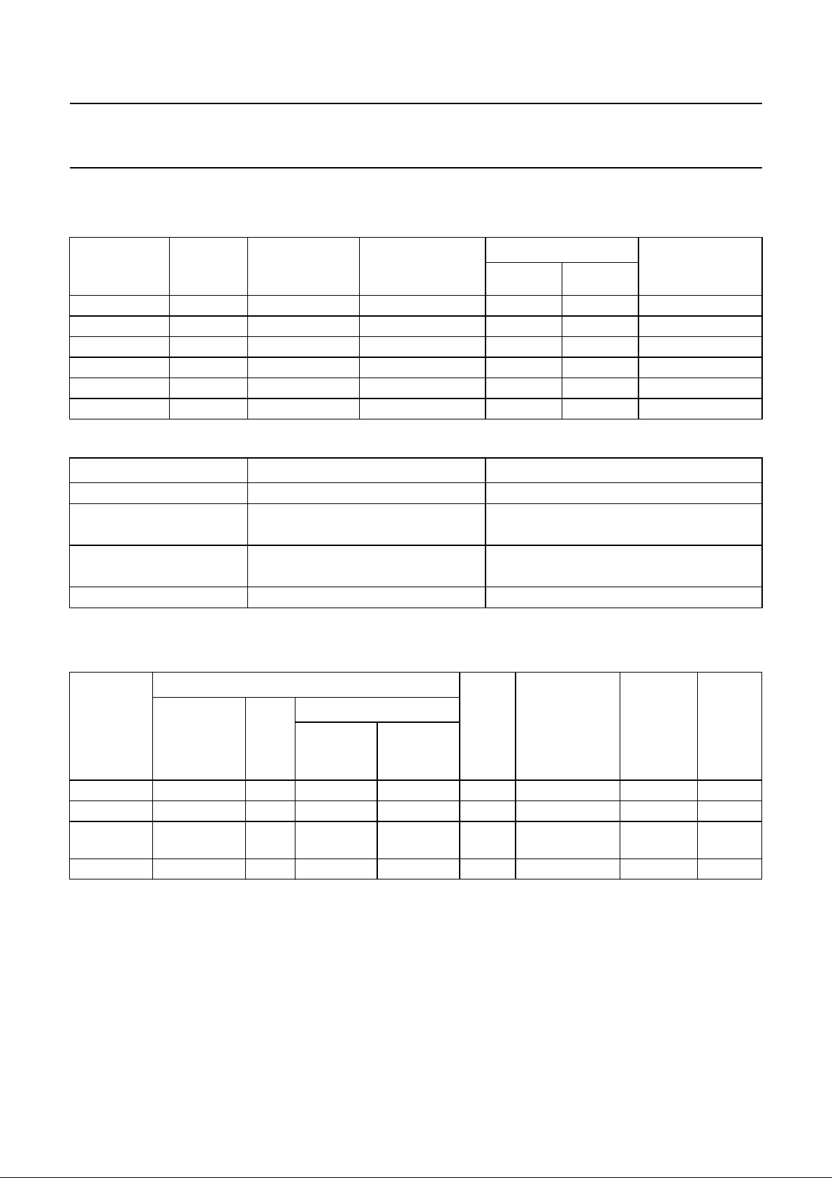
An overview of the supported standards and sound
systems and their key parameters is given in Table 1.
1998 Feb 13 3
Page 4
Philips Semiconductors Preliminary specification
Digital TV Sound Processor (DTVSP) TDA9875
2.1.1 ANALOG 2-CARRIER SYSTEMS
Table 1 Frequency modulation
STANDARD
SOUND
SYSTEM
CARRIER
FREQUENCY
(MHz)
FM DEVIATION
(kHz)
NOM./MAX./OVER
MODULATION BANDWIDTH/
DE-EMPHASIS
SC1 SC2
M mono 4.5 15/25/50 mono − 15/75
M A2+ 4.5/4.724 15/25/50
B/G A2 5.5/5.742 27/50/80
1
⁄2(L + R)1⁄2(L − R) 15/75 (Korea)
1
⁄2(L + R) R 15/50
I mono 6.0 27/50/80 mono − 15/50
D/K A2 6.5/6.742 27/50/80
D/K A2* 6.5/6.26 27/50/80
1
⁄2(L + R) R 15/50
1
⁄2(L + R) R 15/50
Table 2 Identification for A2 systems
PARAMETER A2/A2* A2+ (KOREA)
Pilot frequency 54.6875 kHz = 3.5 × line frequency 55.0699 kHz = 3.5 × line frequency
Stereo identification
frequency
Dual identification frequency
117.5 Hz
274.1 Hz
pilot frequency
= 149.9 Hz
-------------------------------------- 133
pilot frequency
= 276.0 Hz
-------------------------------------- -
57
pilot frequency
=
-------------------------------------- 105
pilot frequency
=
-------------------------------------- -
57
AM modulation depth 50% 50%
2.1.2 2-CARRIER SYSTEMS WITH NICAM
(kHz/µs)
Table 3 NICAM
SC1
SC2
(MHz)
NICAM
DE-EMPHASIS
ROLL-OFF
(%)
STANDARD
FREQUENCY
(MHz)
TYPE
MODULATION
INDEX (%)
NOM/MAX.
DEVIATION
(kHz)
NOM./MAX.
B/G 5.5 FM − 27/50 5.85 J17 40 note 1
I 6.0 FM − 27/50 6.552 J17 100 note 1
D/K 6.5 FM − 27/50 5.85 J17 40 not yet
L 6.5 AM 54/100 − 5.85 J17 40 note 1
Note
1. See
“EBU specification”
or equivalent specification.
NICAM
CODING
defined
1998 Feb 13 4
Page 5
Philips Semiconductors Preliminary specification
Digital TV Sound Processor (DTVSP) TDA9875
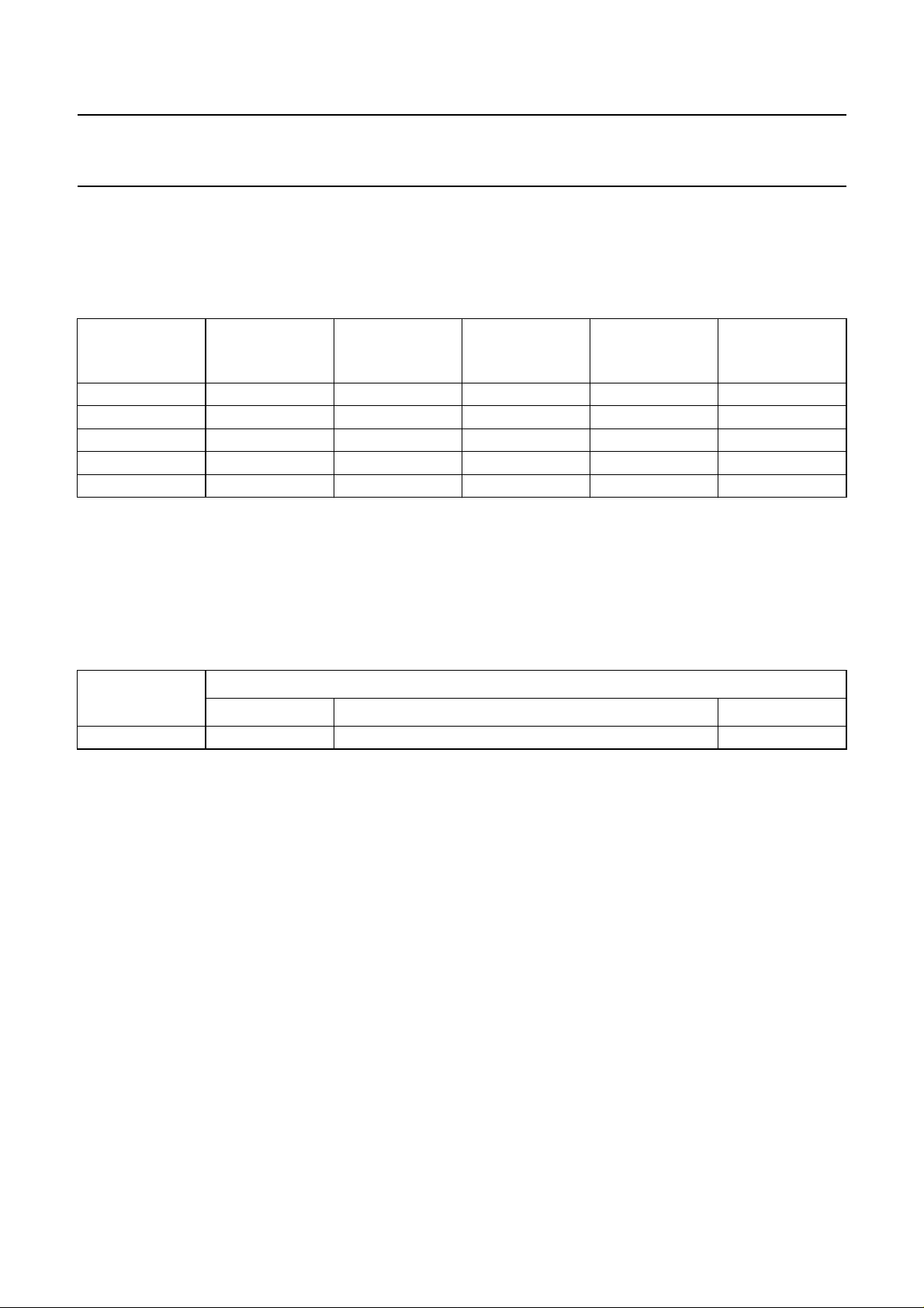
2.1.3 SATELLITE SYSTEMS
An important specification for satellite TV reception is the
“Astra specification”
. The TDA9875 is suited for the reception
of Astra and other satellite signals.
Table 4 FM satellite sound
CARRIER TYPE
Main 6.50
CARRIER
FREQUENCY
(MHz)
(1)
MODULATION
INDEX
0.26 85 mono 15/50
Sub 7.02/7.20 0.15 50 m/st/d
Sub 7.38/7.56 0.15 50 m/st/d
Sub 7.74/7.92 0.15 50 m/st/d
Sub 8.10/8.28 0.15 50 m/st/d
MAXIMUM
FM DEVIATION
(kHz)
MODULATION
(2)
(2)
(2)
(2)
BANDWIDTH/
DE-EMPHASIS
(kHz/µs)
(1)
15/adaptive
15/adaptive
15/adaptive
15/adaptive
(3)
(3)
(3)
(3)
Notes
1. For other satellite systems, frequencies of, for example, 5.80, 6.60 or 6.65 MHz can also be received. A de-emphasis
of 60 µs, or in accordance with J17, is available.
2. m/st/d = mono or stereo or dual language sound.
3. Adaptive de-emphasis = compatible to transmitter specification.
3 ORDERING INFORMATION
PACKAGE
TYPE NUMBER
NAME DESCRIPTION VERSION
TDA9875 SDIP64 plastic shrink dual in-line package; 64 leads (750 mil) SOT274-1
1998 Feb 13 5
Page 6
Philips Semiconductors Preliminary specification
Digital TV Sound Processor (DTVSP) TDA9875
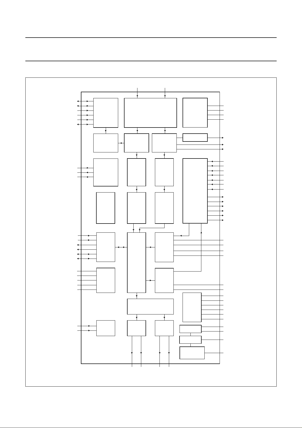
4 BLOCK DIAGRAM
handbook, full pagewidth
ADDR1
ADDR2
SCL
SDA
XTALI
XTALO
SYSCLK
SIF2 SIF1
10 12
9
P1
20
P2
3
13
4
5
18
17
21
I2C-BUS
INTERFACE
IDENTIFICATION
CLOCK
PEAK
DETECTION
INPUT SWITCH
FM (AM)
DEMODULATION
DEMATRIX
LEVEL
ADJUST
AGC, ADC
NICAM
DEMODULATION
NICAM
DECODER
LEVEL
ADJUST
SUPPLY
SOUND IF
(SIF)
TIMING
DETECTION DAC
ANALOG
CROSSBAR
SWITCH
7
V
DDA1
6
V
SSA1
11
V
ref1
8
I
ref
19
V
tune
2
NICAM
1
PCLK
33
SCIR1
34
SCIL1
36
SCIR2
37
SCIL2
31
EXTIR
32
EXTIL
29
MONOIN
47
SCOR1
48
SCOL1
51
SCOR2
52
SCOL2
63
LOR
62
LOL
SDI1
SDI2
SDO1
SDO2
SCK
WS
V
DDD1
V
DDD2
V
SSD1
V
SSD2
CRESET
TEST1
TEST2
27
26
25
24
22
23
15
64
14
49
16
28
30
I2C-BUS
AUDIO
INTERFACE
DIGITAL
SUPPLY
TDA9875
TEST
DIGITAL
SELECT
AUDIO PROCESSING
DAC(2)
61
MOL
MOR60AUXOL58AUXOR
ADC(2)
DAC(2)
DAC(2)
57
SUPPLY
DAC
SUPPLY DAC
REFERENCE
SUPPLY
OPERATIONAL
AMPLIFIERS
42
41
45
44
54
55
38
43
35
46
39
40
59
56
53
50
MGK107
CAPL2
CAPL1
CAPR1
CAPR2
PCAPR
PCAPL
V
DDA2
V
SSA2
V
SSG
V
ref2
V
ref(p)
V
ref(n)
V
DDA3
V
SSA3
V
ref3
V
SSA4
Fig.1 Block diagram.
1998 Feb 13 6
Page 7
Philips Semiconductors Preliminary specification
Digital TV Sound Processor (DTVSP) TDA9875
5 PINNING
SYMBOL PIN I/O DESCRIPTION
PCLK 1 O NICAM clock output at 728 kHz
NICAM 2 O serial NICAM data output at 728 kHz
ADDR1 3 I first I
SCL 4 I I
SDA 5 I/O I
V
V
I
ref
SSA1
DDA1
6 supply supply ground 1; analog front-end circuitry
7 supply analog supply voltage 1; analog front-end circuitry
8 − resistor for reference current generator; analog front-end circuitry
P1 9 I/O first general purpose I/O pin
SIF2 10 I sound IF input 2
V
ref1
11 − reference voltage; analog front-end circuitry
SIF1 12 I sound IF input 1
ADDR2 13 I second I
V
V
SSD1
DDD1
14 supply supply ground 1; digital circuitry
15 supply digital supply voltage 1; digital circuitry
CRESET 16 − capacitor for power-on reset
XTALO 17 O crystal oscillator output
XTALI 18 I crystal oscillator input
V
tune
19 O tuning voltage output for crystal oscillator
P2 20 I/O second general purpose I/O pin
SYSCLK 21 O system clock output
SCK 22 I/O I
WS 23 I/O I
SDO2 24 O I
SDO1 25 O I
SDI2 26 I I
SDI1 27 I I
TEST1 28 I first test pin; connected to V
MONOIN 29 I audio mono input
TEST2 30 I second test pin; connected to V
EXTIR 31 I external audio input right channel
EXTIL 32 I external audio input left channel
SCIR1 33 I SCART 1 input right channel
SCIL1 34 I SCART 1 input left channel
V
SSG
35 − ground guards; audio analog-to-digital converter circuitry
SCIR2 36 I SCART 2 input right channel
SCIL2 37 I SCART 2 input left channel
V
V
V
DDA2
ref(p)
ref(n)
38 supply analog supply voltage 2; audio analog-to-digital converter circuitry
39 − positive reference voltage; audio analog-to-digital converter circuitry
40 − reference voltage ground; audio analog-to-digital converter circuitry
2
C-bus slave address modifier
2
C-bus clock
2
C-bus data
2
C-bus slave address modifier
2
S-bus clock
2
S-bus word select
2
S-bus data output 2
2
S-bus data output 1
2
S-bus data input 2
2
S-bus data input 1
for normal operation
SSD1
for normal operation
SSD1
1998 Feb 13 7
Page 8

Philips Semiconductors Preliminary specification
Digital TV Sound Processor (DTVSP) TDA9875
SYMBOL PIN I/O DESCRIPTION
CAPL1 41 − filter capacitor pin 1; audio analog-to-digital converter, left channel
CAPL2 42 − filter capacitor pin 2; audio analog-to-digital converter, left channel
V
SSA2
CAPR2 44 − filter capacitor pin 2; audio analog-to-digital converter, right channel
CAPR1 45 − filter capacitor pin 1; audio analog-to-digital converter, right channel
V
ref2
SCOR1 47 O SCART 1 output right channel
SCOL1 48 O SCART 1 output left channel
V
SSD2
V
SSA4
SCOR2 51 O SCART 2 output right channel
SCOL2 52 O SCART 2 output left channel
V
ref3
PCAPR 54 − post-filter capacitor pin right channel, audio digital-to-analog converter
PCAPL 55 − post-filter capacitor pin left channel, audio digital-to-analog converter
V
SSA3
AUXOR 57 O headphone (Auxiliary) output right channel
AUXOL 58 O headphone (Auxiliary) output left channel
V
DDA3
MOR 60 O loudspeaker (Main) output right channel
MOL 61 O loudspeaker (Main) output left channel
LOL 62 O line output left channel
LOR 63 O line output right channel
V
DDD2
43 supply supply ground 2; audio analog-to-digital converter circuitry
46 − reference voltage; audio analog-to-digital converter circuitry
49 supply supply ground 2; digital circuitry
50 supply supply ground 4; audio operational amplifier circuitry
53 − reference voltage; audio digital-to-analog converter and operational amplifier
circuitry
56 supply supply ground 3; audio digital-to-analog converter circuitry
59 supply analog supply voltage 3; audio digital-to-analog converter
64 supply digital supply voltage 2; digital circuitry
1998 Feb 13 8
Page 9
Philips Semiconductors Preliminary specification
Digital TV Sound Processor (DTVSP) TDA9875
handbook, halfpage
PCLK
NICAM
ADDR1
SCL
SDA
V
SSA1
V
DDA1
I
ref
P1
SIF2
V
ref1
SIF1
ADDR2
V
SSD1
V
DDD1
CRESET
XTALO
XTALI
V
tune
P2
SYSCLK
SCK
WS
SDO2
SDO1
SDI2
SDI1
TEST1
MONOIN
TEST2
EXTIR
EXTIL
1
2
3
4
5
6
7
8
9
10
11
12
13
14
15
16
17
18
19
20
21
22
23
24
25
26
27
28
29
30
31
32
TDA9875
MGK106
64
63
62
61
60
59
58
57
56
55
54
53
52
51
50
49
48
47
46
45
44
43
42
41
40
39
38
37
36
35
34
33
V
DDD2
LOR
LOL
MOL
MOR
V
DDA3
AUXOL
AUXOR
V
SSA3
PCAPL
PCAPR
V
ref3
SCOL2
SCOR2
V
SSA4
V
SSD2
SCOL1
SCOR1
V
ref2
CAPR1
CAPR2
V
SSA2
CAPL2
CAPL1
V
ref(n)
V
ref(p)
V
DDA2
SCIL2
SCIR2
V
SSG
SCIL1
SCIR1
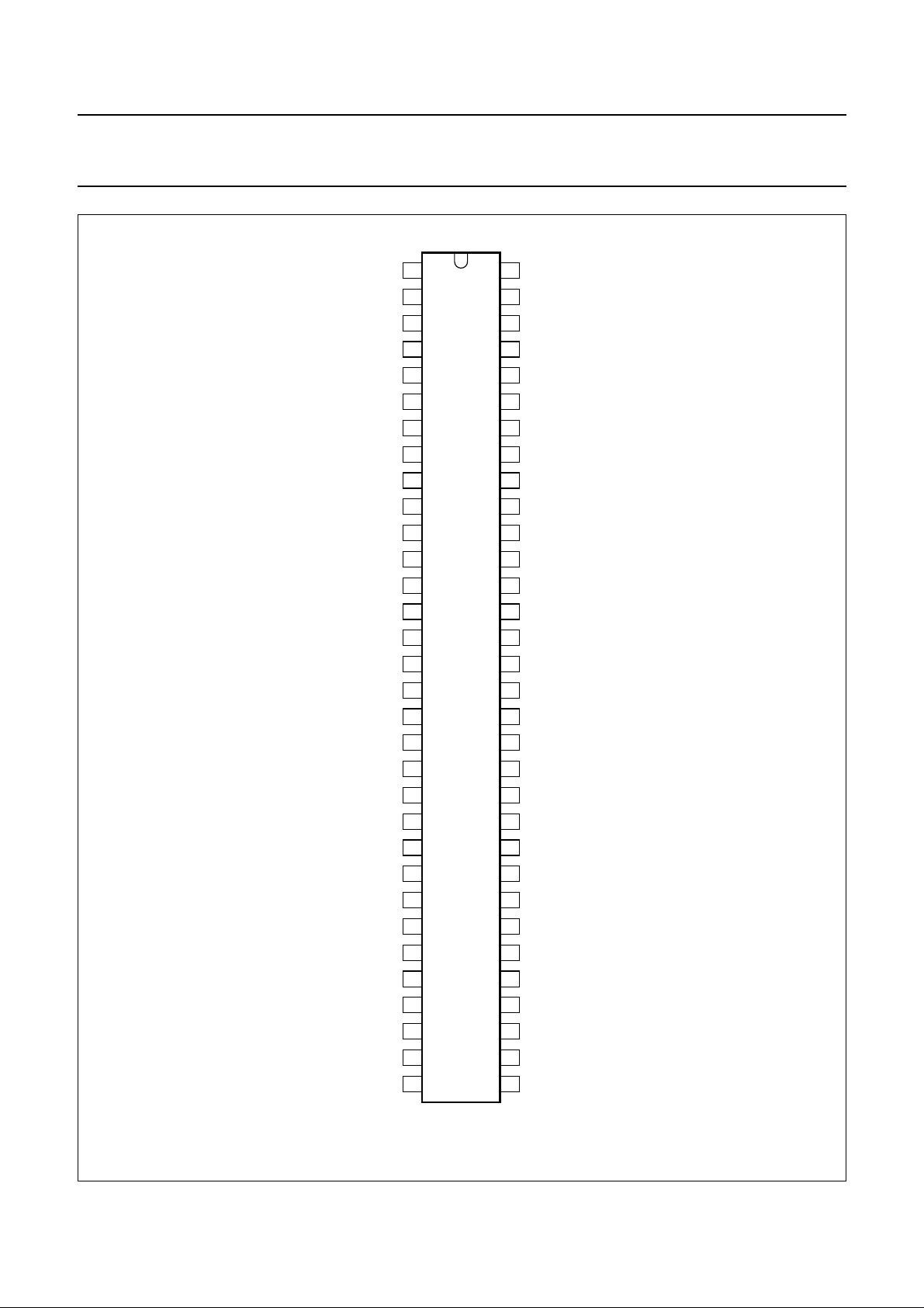
Fig.2 Pin configuration.
1998 Feb 13 9
Page 10

Philips Semiconductors Preliminary specification
Digital TV Sound Processor (DTVSP) TDA9875
6 FUNCTIONAL DESCRIPTION
6.1 Description of the demodulator and decoder section
6.1.1 SIF
INPUT
Two input pins are provided, SIF1 e.g. for terrestrial TV
and SIF2 e.g. for a satellite tuner. As no specific filters are
integrated, both inputs have the same specification giving
flexibility in application. The selected signal is passed
through an AGC circuit and then digitized by an 8-bit ADC
operating at 24.576 MHz.
6.1.2 AGC
The gain of the AGC amplifier is controlled from the ADC
output by means of a digital control loop employing
hysteresis. The AGC has a fast attack behaviour to
prevent ADC overloads and a slow decay behaviour to
prevent AGC oscillations. For AM demodulation the AGC
must be switched off. When switched off, the control loop
is reset and fixed gain settings can be chosen from
Table 12 (subaddress 0).
The AGC can be controlled via the I
2
C-bus. Details can be
found in the I2C-bus register definitions (see Chapter 10).
6.1.3 M
IXER
The digitized input signal is fed to the mixers, which mix
one or both input sound carriers down to zero IF. A 24-bit
control word for each carrier sets the required frequency.
Access to the mixer control word registers is via the
I2C-bus. When receiving NICAM programs, a feedback
signal is added to the control word of the second carrier
mixer to establish a carrier-frequency loop.
6.1.4 FM
AND AM DEMODULATION
An FM or AM input signal is fed via a band-limiting filter to
a demodulator that can be used for either FM or AM
demodulation. Apart from the standard (fixed)
de-emphasis characteristic, an adaptive de-emphasis is
available for encoded satellite programs. A stereo decoder
recovers the left and right signal channels from the
demodulated sound carriers. Both the European and
Korean stereo systems are supported.
6.1.5 FM
IDENTIFICATION
The identification of the FM sound mode is performed by
AM synchronous demodulation of the pilot signal and
narrow-band detection of the identification frequencies.
The result is available via the I2C-bus interface. A selection
can be made via the I2C-bus for B/G, D/K and M standard
and for three different modes that represent different
trade-offs between speed and reliability of identification.
6.1.6 NICAM
DEMODULATION
The NICAM signal is transmitted in a DQPSK code at a bit
rate of 728 kbit/s. The NICAM demodulator performs
DQPSK demodulation and feeds the resulting bitstream
and clock signal onto the NICAM decoder and, for
evaluation purposes, to PCLK (pin 1) and NICAM (pin 2).
A timing loop controls the frequency of the crystal oscillator
to lock the sampling rate to the symbol timing of the
NICAM data. The polarity of the control signal is selectable
to support applications in which external circuitry is used to
boost the tuning voltage of the oscillator.
6.1.7 NICAM
DECODER
The device performs all decoding functions in accordance
with the
“EBU NICAM 728 specification”
. After locking to
the frame alignment word, the data is descrambled by
applying the defined pseudo-random binary sequence;
the device will then synchronize to the periodic frame flag
bit C0.
The status of the NICAM decoder can be read out from the
2
NICAM status register by the user (see the I
C-bus
register description in Section 10.4.2). The OSB bit
indicates that the decoder has locked to the NICAM data.
The VDSP bit indicates that the decoder has locked to the
NICAM data and that the data is valid sound data. The C4
bit indicates that the sound conveyed by the FM mono
channel is identical to the sound conveyed by the NICAM
channel. The error byte contains the number of sound
sample errors, resulting from parity checking, that
occurred in the past 128 ms period. The Bit Error Rate
(BER) can be calculated using the following equation;
BER
bit errors
----------------------total bits
error byte 1.74× 10
5–
×≈=
1998 Feb 13 10
Page 11

Philips Semiconductors Preliminary specification
Digital TV Sound Processor (DTVSP) TDA9875
6.1.8 NICAM AUTO-MUTE
This function is enabled by setting bit AMUTE LOW
subaddress 14 (see Section 10.3.11). Upper and lower
error limits may be defined by writing appropriate values to
two registers in the I2C-bus section (subaddresses 16 and
17; see Sections 10.3.13 and 10.3.14). When the number
of errors in a 128 ms period exceeds the upper error limit
the auto-mute function will switch the output sound from
NICAM to whatever sound is on the first sound carrier
(FM or AM). When the error count is smaller than the lower
error limit the NICAM sound is restored.
The auto-mute function can be disabled by setting bit
AMUTE HIGH. In this condition clicks become audible
when the error count increases; the user will hear a signal
of degrading quality.
A decision to enable/disable the auto-muting is taken by
the microcontroller based on an interpretation of the
application control bits C1, C2, C3 and C4 and, possibly,
any additional strategy implemented by the set maker in
the microcontroller software.
When the AM sound in NICAM L systems is demodulated
in the 1st sound IF and the audio signal connected to the
mono input of the TDA9875, the controlling microcontroller
must implement the switching from NICAM reception to
mono input, if auto-muting is desired.
6.1.9 CRYSTAL OSCILLATOR
A circuit diagram of the external components of the
voltage-controlled crystal oscillator is illustrated in Fig.8
(see Chapter 12).
6.1.10 T
Both test pins are active HIGH, in normal operation of the
device they are wired to V
manufacturing tests only and are not available to
customers. Without external circuitry these pads are pulled
down to LOW level with internal resistors.
EST PINS
. Test functions are for
SSD1
1998 Feb 13 11
Page 12
This text is here in white to force landscape pages to be rotated correctly when browsing through the pdf in the Acrobat reader.This text is here in
d
_white to force landscape pages to be rotated correctly when browsing through the pdf in the Acrobat reader.This text is here inThis text is here in
white to force landscape pages to be rotated correctly when browsing through the pdf in the Acrobat reader. white to force landscape pages to be ...
1998 Feb 13 12
FM
2
DC
FILTER
from ADC
2
I
2
I
NICAM
ADAPTIVE
DE-EMPHASIS
S1
S2
2
DC
FILTER
2
2
2
FIXED
DE-EMPHASIS
FIXED
DE-EMPHASIS
LEVEL ADJUST
2
LEVEL ADJUST
LEVEL ADJUST
LEVEL ADJUST
LEVEL ADJUST
MATRIX
2 2 2
2
4
6
8
10
book, full pagewidth
DIGITAL
CROSSBAR
SELECT
2
2
2
2
2
MATRIX
MATRIX
MATRIX
MATRIX
MATRIX
AUTOMATIC
VOLUME
LEVEL
VOLUME
SOFT-MUTE
BASS/TREBLE
BEEPER
LEVEL ADJUST AND MUTE
LEVEL ADJUST AND MUTE
LEVEL ADJUST
BASS/TREBLE
SPA TIAL
PSEUDO
VOLUME
BASS BOOST
CONTOUR
SOFT-MUTE
BEEPER
2
2
2
2
2
LS
HP
2
S1
I
2
I
S2
DAC
6.2 Description of the DSP
Philips Semiconductors Preliminary specification
Digital TV Sound Processor (DTVSP) TDA9875
2 4
12
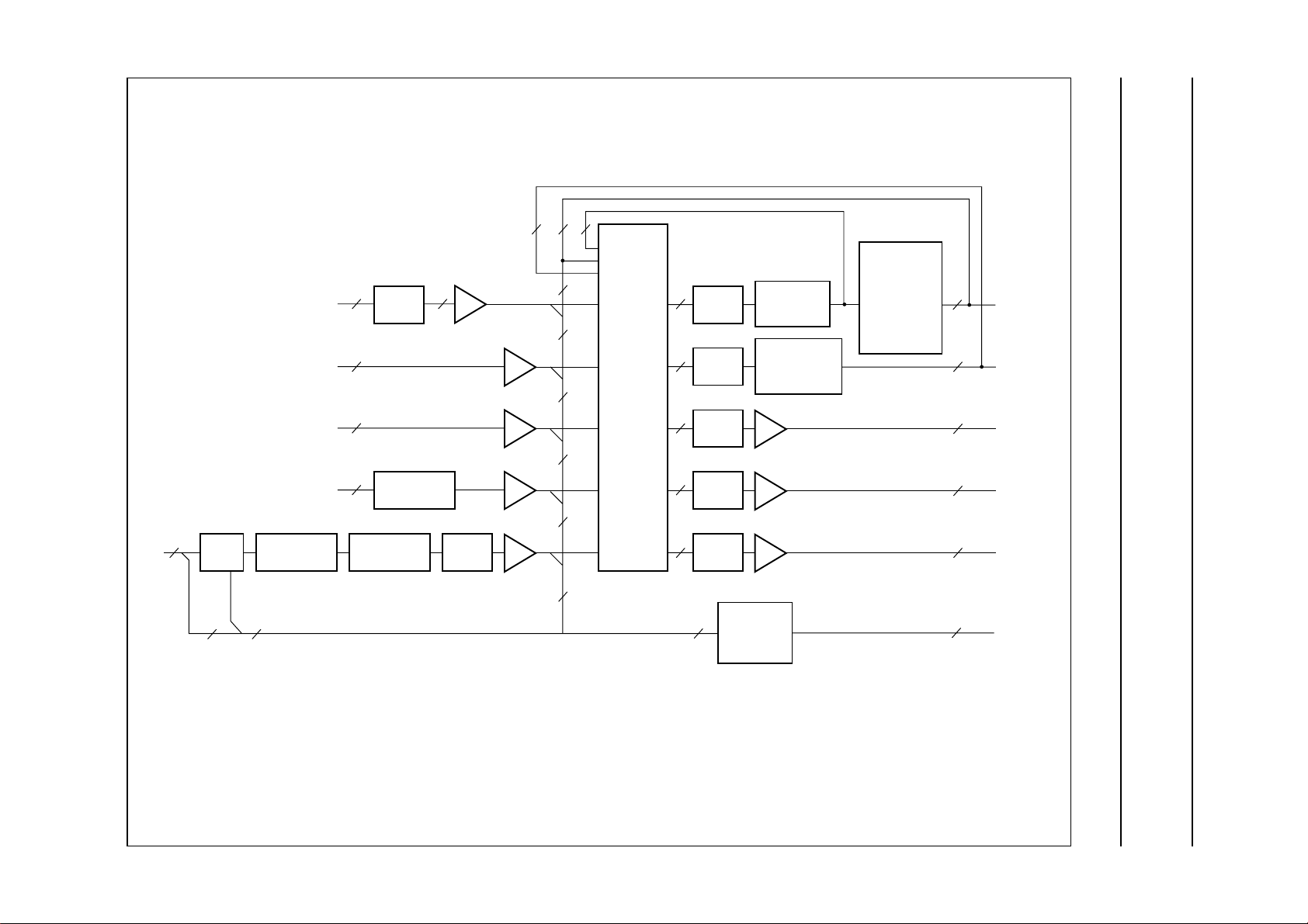
Fig.3 DSP data flow diagram.
16
MONITOR
SELECT
PEAK
DETECTION
1
2
I
C-bus
MGK108
Page 13

Philips Semiconductors Preliminary specification
Digital TV Sound Processor (DTVSP) TDA9875
6.2.1 LEVEL SCALING
All input channels to the digital crossbar switch (except for
the loudspeaker feedback path) are equipped with a level
adjust facility to change the signal level in a range of
±15 dB. It is recommended to scale all input channels to be
15 dB below full-scale (−15 dB full-scale) under nominal
conditions.
6.2.2 NICAM
PATH
The NICAM path has a switchable J17 de-emphasis.
6.2.3 FM (AM)
PATH
A high-pass filter suppresses DC offsets from the
FM demodulator due to carrier frequency offsets and
supplies the monitor/peak function with DC values and an
unfiltered signal, e.g. for the purpose of carrier detection.
The de-emphasis function offers fixed settings for the
supported standards (50 µs, 60 µs, 75 µs and J17).
An adaptive de-emphasis is available for
Wegener-Panda 1 encoded programs.
A matrix performs the dematrixing of1⁄2(L + R) and
R to L and R signals, of1⁄2(L + R) and1⁄2(L − R) to L and R
signals or of channel 1 and channel 2 to L and R signals.
6.2.4 NICAM
AUTO-MUTE
If NICAM is received and the signal quality becomes poor,
the digital crossbar switch switches automatically to FM
and switches the matrix to channel 1. The automatic
switching between NICAM and channel 1 (FM or AM)
reception depends on the NICAM bit error rate.
The auto-mute function can be disabled via the I2C-bus.
6.2.5 M
ONITOR
This function provides data words from a number of
locations of the signal processing paths to the I2C-bus
interface (2 data bytes). Signal sources include the
FM demodulator outputs, most inputs to the digital
crossbar switch and the inputs to the loudspeaker channel
of the ADC. Source selection and data read-out is
performed via the I2C-bus.
Optionally, the peak value can be measured instead of
simply taking samples. The internally stored peak value is
reset to zero when the data is read via the I2C-bus.
The monitor function may be used, for example, for signal
level measurements or carrier detection.
6.2.6 L
OUDSPEAKER (MAIN) CHANNEL
The matrix provides the following functions; forced mono,
stereo, channel swap, channel 1, channel 2 and spatial
effects.
There are fixed coefficient sets for spatial settings of 30%,
40% and 52%.
The Automatic Volume Level (AVL) function provides a
constant output level of −23 dB full-scale for input levels
between 0 dBFS and −29 dB full-scale. There are some
fixed decay time constants to choose from, i.e. 2, 4 and
8 seconds.
Pseudo stereo is based on a phase shift in one channel via
a 2nd-order all-pass filter. There are fixed coefficient sets
to provide 90 degrees phase shift at frequencies of
150, 200 and 300 Hz.
Volume is controlled individually for each channel ranging
from +24 dB to −83 dB with 1 dB resolution. There is also
a mute position. For the purpose of a simple control
software in the microcontroller, the decimal number that is
2
sent as an I
C-bus data byte for volume control is identical
to the volume setting in dBs (e.g. the I2C-bus data
byte +10 sets the new volume value to +10 dB).
Balance can be realized by independent control of the left
and right channel volume settings.
Contour is adjustable between 0 dB and +18 dB with 1 dB
resolution.
Bass is adjustable between +15 dB and −12 dB with 1 dB
resolution and treble is adjustable between ±12 dB with
1 dB resolution.
For the purpose of a simple control software in the
microcontroller, the decimal number that is sent as an
I2C-bus data byte for contour, bass or treble is identical to
the new contour, bass or treble setting in dBs (e.g. the
I2C-bus data byte +8 sets the new value to +8 dB).
Extra bass boost is provided up to 20 dB with 2 dB
resolution. The implemented coefficient set serves merely
as an example on how to use this filter.
The beeper provides tones in a range from approximately
400 Hz to 30 kHz. The frequency can be selected via the
I2C-bus. The beeper output signal is added to the
loudspeaker and headphone channel signals. The beeper
volume is adjustable with respect to full-scale between
0 dB and −93 dB with a 3 dB step resolution. The beeper
is not effected by mute.
1998 Feb 13 13
Page 14

Philips Semiconductors Preliminary specification
Digital TV Sound Processor (DTVSP) TDA9875
Soft-mute provides a mute ability in addition to volume
control with a well defined time (32 ms) after which the
soft-mute is completed. A smooth fading is achieved by a
cosine masking.
6.2.7 H
EADPHONE (AUXILIARY) CHANNEL
The matrix provides the following functions; forced mono,
stereo, channel swap, channel 1 and channel 2
(or C and S in Dolby Surround Pro Logic mode).
Volume is controlled individually for each channel in a
range from +24 to −83 dB with 1 dB resolution. There is
also a mute position. For the purpose of a simple control
software in the microcontroller, the decimal number that is
2
sent as an I
C-bus data byte for volume control is identical
to the volume setting in dBs (e.g. the I2C-bus data
byte +10 sets the new volume value to +10 dB).
Balance can be realized by independent control of the left
and right channel volume settings.
Bass is adjustable between +15 dB and −12 dB with 1 dB
resolution and treble is adjustable between ±12 dB with
1 dB resolution.
For the purpose of a simple control software in the
microcontroller, the decimal number that is sent as an
I2C-bus data byte for bass or treble is identical to the new
bass or treble setting in dB (e.g. the I2C-bus data byte +8
sets the new value to +8 dB).
The beeper provides tones in a range from approximately
400 Hz to 30 kHz. The frequency can be selected via the
I2C-bus. The beeper output signal is added to the
loudspeaker and headphone channel signals. The beeper
volume is adjustable with respect to full-scale between
0 dB and −93 dB with a 3 dB step resolution. The beeper
is not effected by mute.
Soft-mute provides a mute ability in addition to volume
control with a well defined time (32 ms) after which the
soft-mute is completed. A smooth fading is achieved by a
cosine masking.
6.2.8 F
EATURE INTERFACE
The feature interface comprises two I2S-bus input/output
ports and a system clock output. Each I2S-bus port is
equipped with level adjust facilities that can change the
signal level in a ±15 dB range in 1 dB steps. Outputs can
be disabled to improve EMC performance.
The I2S-bus output matrix provides the following functions;
forced mono, stereo, channel swap, channel 1 and
channel 2.
One example of how the feature interface can be used in
a TV set is to connect an external Dolby Surround Pro
Logic DSP, such as the SAA7710, to the I
2
S-bus ports.
Outputs must be enabled and a suitable master clock
signal for the DSP can be taken from pin SYSCLK.
A stereo signal from any source will be output on one of
the I2S-bus serial data outputs and the four processed
signal channels will be entered at both I2S-bus serial data
inputs. Left and right could then be output to the power
amplifiers via the Main channel, centre and surround via
the Auxiliary channel.
6.2.9 C
HANNEL FROM THE AUDIO ANALOG-TO-DIGITAL
CONVERTER
The signal level at the output of the ADC can be adjusted
in a range of±15 dB with a 1 dB step resolution. The audio
ADC itself is scaled to a gain of −6 dB.
6.2.10 C
HANNEL TO THE ANALOG CROSSBAR PATH
Level adjust with control positions 0 dB, +3 dB, +6 dB
and +9 dB.
6.2.11 D
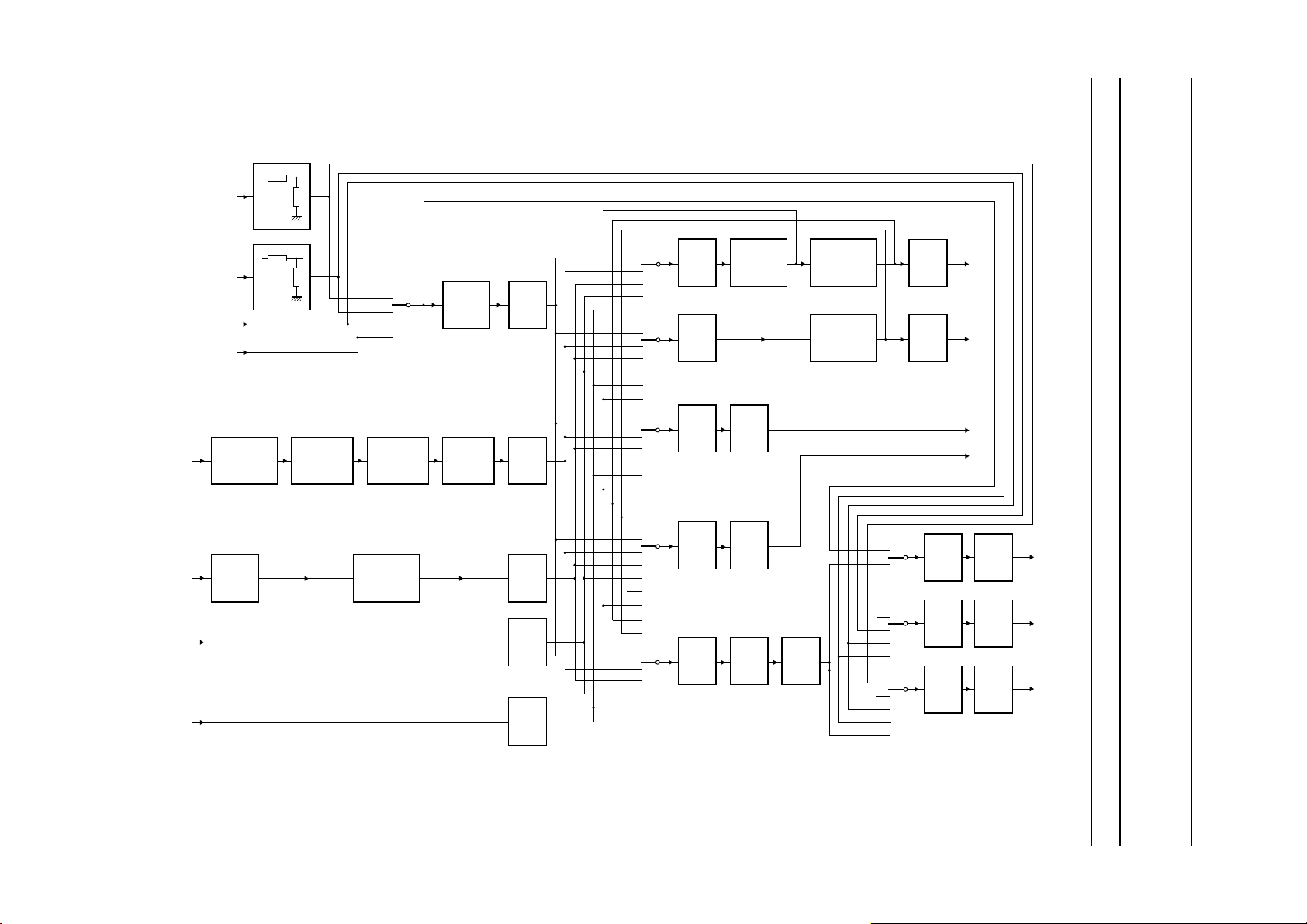
IGITAL CROSSBAR SWITCH (SEE Fig.6)
Input channels to the crossbar switch are from the audio
ADC, I2S1, I2S2, FM path, NICAM path and from the
loudspeaker channel path after matrix and AVL.
Output channels comprise loudspeaker, headphone, I2S1,
I2S2 and the audio DACs for line output and SCART.
The I2S1 and I2S2 outputs also provide digital outputs from
the loudspeaker and headphone channels, but without the
beeper signals.
6.2.12 G
ENERAL
There are a number of functions that can provide signal
gain, e.g. volume, bass and treble control. Great care has
to be taken when using gain with large input signals in
order not to exceed the maximum possible signal swing,
which would cause severe signal distortion. The nominal
signal level of the various signal sources to the digital
crossbar switch should be 15 dB below digital full-scale
(−15 dB full-scale). This means that a volume setting of,
say, +15 dB would just produce a full-scale output signal
and not cause clipping, if the signal level is nominal.
Sending illegal data patterns via the I2C-bus will not cause
any changes of the current setting for the volume, bass,
treble, bass boost and level adjust functions.
1998 Feb 13 14
Page 15
Philips Semiconductors Preliminary specification
Digital TV Sound Processor (DTVSP) TDA9875
6.2.13 EXPERT MODE
The TDA9875 provides a special expert mode that gives direct write access to the internal Coefficient RAM (CRAM) of
the DSP. It can be used to create user-defined characteristics, such as a tone control with different corner frequencies
or special boost/cut characteristics to correct the low-frequency loudspeaker and/or cabinet frequency responses by
means of the bass boost filter. However, this mode must be used with great care.
More information on the functions of this device, such as filter structures, the number of coefficients per function, their
default values, memory addresses, etc., can be made available on request.
6.2.14 DSP
Table 5 DSP characteristics
Bass control for loudspeaker and
headphone output
Treble control for loudspeaker
and headphone output
Contour for loudspeaker output
Bass boost for loudspeaker
output
Volume control for each separate
channel in loudspeaker and
headphone output
Soft-mute for loudspeaker and
headphone output
Spatial effects yes anti-phase crosstalk positions 30, 40 and 52 %
Pseudo stereo yes 90 degree phase shift at frequency 150, 200 and 300 Hz
Beeper additional to the signal in
the loudspeaker and headphone
channel
AVL
General
CHARACTERISTICS
FUNCTION
EXPERT
MODE
yes
yes
yes
yes
no
no
yes
no
no
PARAMETER VALUE UNIT
control range −12 to +15 dB
step resolution 1 dB
step resolution at frequency 40 Hz
control range −12 to +12 dB
step resolution 1 dB
step resolution at frequency 14 kHz
control range 0 to +18 dB
step resolution 1 dB
step resolution at frequency 40 Hz
control range 0 to +20 dB
step resolution 2 dB
step resolution at frequency 20 Hz
corner frequency 350 Hz
control range −83 to +24 dB
step resolution 1 dB
mute position at step 10101100
processing time 32 ms
beep frequencies see Section 10.3.38
control range 0 to −93 dB
step resolution 3 dB
mute position at step 00100000
step width quasi continuously
AVL output level for an input level
between 0 dB and −29 dB (full-scale)
attack time 10 ms
decay time constant 2, 4 and 8 s
−3 dB lower corner frequency of DSP 10 Hz
−1 dB bandwidth of DSP 14.5 kHz
−23 dB
1998 Feb 13 15
Page 16
Philips Semiconductors Preliminary specification
Digital TV Sound Processor (DTVSP) TDA9875
FUNCTION
Level adjust I
Level adjust I
outputs
2
S1 and I2S2 inputs
2
S1 and I2S2
EXPERT
MODE
yes
yes
PARAMETER VALUE UNIT
control range −15 to +15 dB
step resolution 1 dB
control range −15 to +15 dB
step resolution 1 dB
mute position at step 00010000
Level adjust analog crossbar path no control positions 0, 3, 6 and 9 dB
Level adjust audio ADC outputs
Level adjust NICAM path
Level adjust FM path
yes
yes
yes
control range +15 to −15 dB
step resolution 1 dB
control range +15 to −15 dB
step resolution 1 dB
control range +15 to −15 dB
step resolution 1 dB
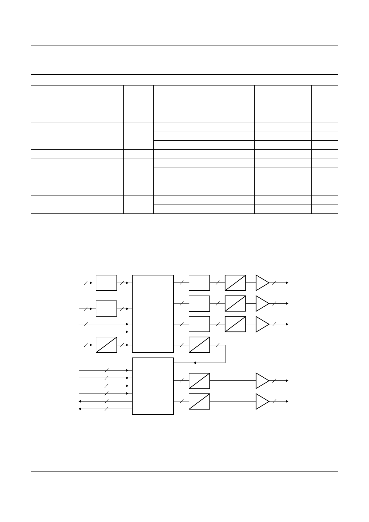
6.3 Description of the analog audio section
handbook, full pagewidth
SCART 1
SCART 2
external
mono
NICAM
I
I
I
I
2
2
2
2
FM
S1
S2
S1
S2
2
−3 dB
2
−3 dB
2
2
D
2
2
2
A
2
2
2
2
2
2
ANALOG
CROSSBAR
SWITCH
DSP
AND
DIGITAL
CROSSBAR
SWITCH
2
2
2
2
2
2
ANALOG
MATRIX
ANALOG
MATRIX
ANALOG
MATRIX
A
D
D
A
D
A
3 dB
2 2
0 dB
3 dB
2
0 dB
3 dB
2
0 dB
2
SCART 1
2
SCART 2
2
Line output
2
Main
2
Auxiliary
MGK109
Fig.4 Block diagram for the audio section.
1998 Feb 13 16
Page 17
Philips Semiconductors Preliminary specification
Digital TV Sound Processor (DTVSP) TDA9875
6.3.1 ANALOG CROSSBAR SWITCH AND ANALOG MATRIX
(see also Fig.6)
There are a number of analog input and output ports with
the TDA9875. Analog source selector switches are
employed to provide the desired analog signal routing
capability. The analog signal routing is performed by the
analog crossbar switch section. A dual audio ADC
provides the connection to the DSP section and a dual
audio DAC provides the connection from the DSP section
to the analog crossbar switch. The digital signal routing is
performed by a digital crossbar switch.
The basic signal routing philosophy of the TDA9875 is that
each switch handles two signal channels at the same time,
e.g. left and right, language A and B, directly at the source.
Each source selector switch is followed by an analog
matrix to perform further selection tasks, such as putting a
signal from one input channel, say language A, to both
output channels or for swapping left and right channels.
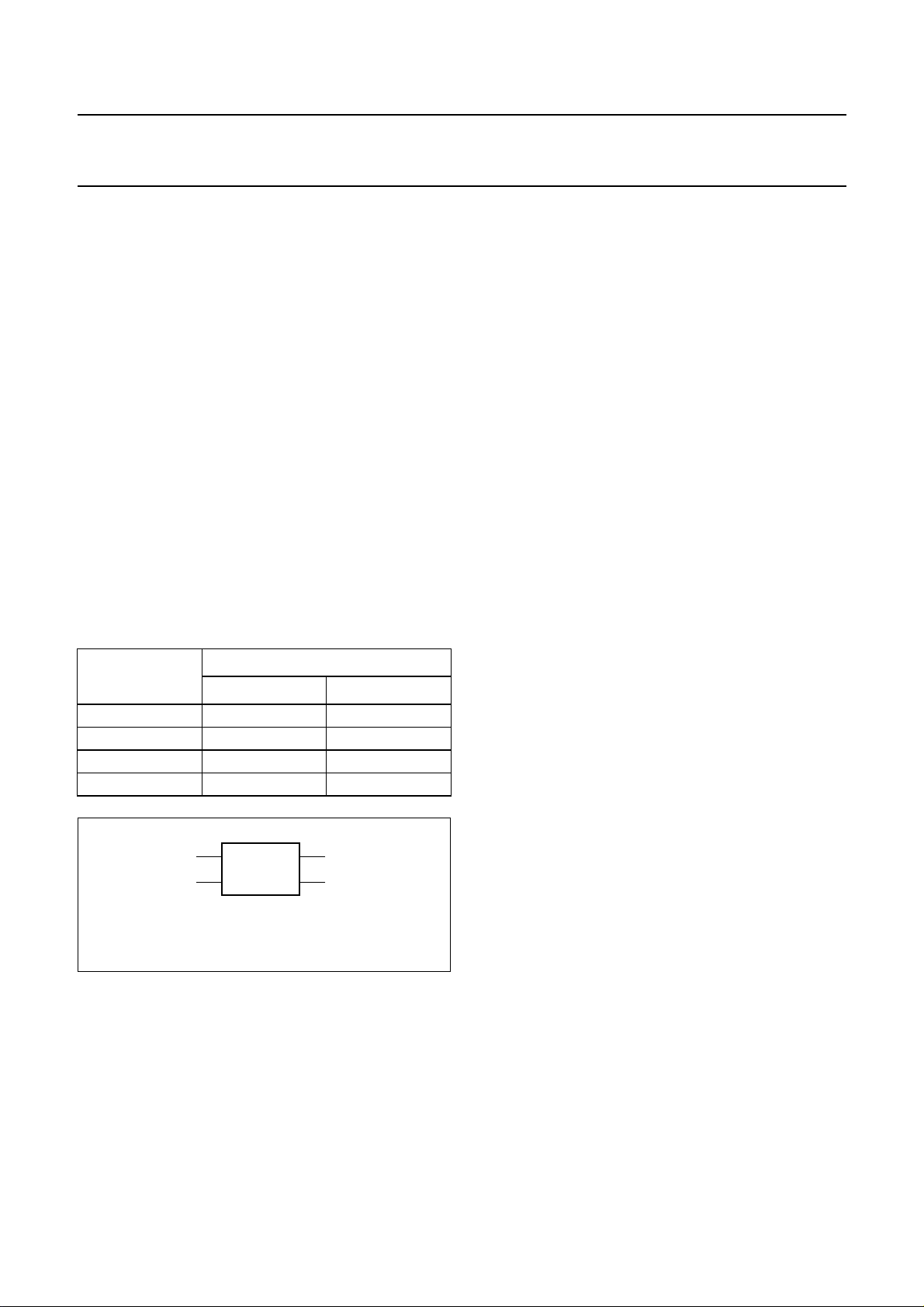
The analog matrix provides the functions given in Table 6
(see also Fig.5).
Table 6 Analog matrix functions
MATRIX OUTPUT
MODE
LEFT OUTPUT RIGHT OUTPUT
1 left input right input
2 right input left input
3 left input left input
4 right input right input
handbook, halfpage
left input
right input
ANALOG
MATRIX
left output
right output
MGK110
Fig.5 Analog matrix.
All switches and matrices are controlled via the I
2
C-bus.
There is one restriction for switching signals at inputs and
outputs for SCART 1 and SCART 2. At these ports, an
input signal cannot be copied to its own output, i.e. it is not
possible to make a copy from SCART 1 input to SCART 1
output.
6.3.2 SCART INPUTS
The SCART specification allows for a signal level of up to
2 V (RMS). Because of signal handling limitations, due to
the 5 V supply voltage of the TDA9875, it is necessary to
have fixed 3 dB attenuators at the SCART inputs to obtain
a 2 V input. This results in a −3 dB SCART-to-SCART
copy gain. If 0 dB copy gain is preferred (with maximum
1.4 V input), there are +3 dB/0 dB amplifiers at the outputs
of SCART 1 and SCART 2 and at the line output.
The input attenuator is realized by an external series
resistor in combination with the input impedance, both of
which form a voltage divider. With this voltage divider the
maximum SCART signal level of 2 V (RMS) is scaled
down to 1.4 V (RMS) at the input pin. If it is known for
certain applications that the input signal level is always
below 1.4 V (RMS), the SCART inputs can be used
without external resistors.
6.3.3 E
XTERNAL AND MONO INPUTS
The 3 dB input attenuators are not required for the external
and mono inputs, because those signal levels are under
control of the TV designer. The maximum allowed input
level is 1.4 V (RMS). By adding external series resistors,
the external inputs can be used as an additional SCART
input.
6.3.4 SCART
OUTPUTS
The SCART outputs employ amplifiers with two gain
settings. The gain can be set to +3 dB or to 0 dB via the
I2C-bus. The +3 dB position is needed to compensate for
the 3 dB attenuation at the SCART inputs should
SCART-to-SCART copies with 0 dB gain be preferred
[under the condition of 1.4 V (RMS) maximum input level].
The 0 dB position is needed, for example, for an
external-to-SCART copy with 0 dB gain.
6.3.5 L
INE OUTPUT
The line output can provide an unprocessed copy of the
audio signal in the loudspeaker channels. This can be
either an external signal that comes from the dual audio
ADC, or a signal from an internal digital audio source that
comes from the dual audio DAC. The line output employs
amplifiers with two gain settings. The +3 dB position is
needed to compensate for the attenuation at the
SCART inputs, while the 0 dB position is needed, for
example, for non-attenuated external or internal digital
signals (see Section 6.3.4).
1998 Feb 13 17
Page 18

Philips Semiconductors Preliminary specification
Digital TV Sound Processor (DTVSP) TDA9875
6.3.6 LOUDSPEAKER (MAIN) AND HEADPHONE
(AUXILIARY) OUTPUTS
Signals from any audio source can be applied to the
loudspeaker and to the headphone output channels via the
digital crossbar switch and the DSP.
6.3.7 D
UAL AUDIO DAC
The TDA9875 contains three dual audio DACs, one for the
connection from the DSP to the analog crossbar switch
section and two for the loudspeaker and headphone
outputs. Each of the three dual low-noise high-dynamic
range DACs consists of two 15-bit DACs with current
outputs, followed by a buffer operational amplifier.
The audio DACs operate with four-fold oversampling and
noise shaping.
6.3.8 D
UAL AUDIO ADC
There is one dual audio ADC in the TDA9875 for the
connection of the analog crossbar switch section to the
DSP. The dual audio ADC consists of two bitstream
3rd-order sigma-delta audio ADCs and a high-order
decimation filter.
6.3.9 S
TANDBY MODE
The standby mode (subaddress 1, bit 5) disables most
functions and reduces power dissipation. The analog
crossbar switch and the SCART section remains
operational and can be controlled by the I2C-bus to
support copying of analog signals from SCART 1 to
SCART 2 and vice versa.
Unused internal registers may lose their information in
standby mode. Therefore, the device needs to be
initialized on returning to normal operation. This can be
accomplished in the same way as after a power-on reset.
1998 Feb 13 18
Page 19
This text is here in white to force landscape pages to be rotated correctly when browsing through the pdf in the Acrobat reader.This text is here in
a
_white to force landscape pages to be rotated correctly when browsing through the pdf in the Acrobat reader.This text is here inThis text is here in
white to force landscape pages to be rotated correctly when browsing through the pdf in the Acrobat reader. white to force landscape pages to be ...
1998 Feb 13 19
SCART 1
ndbook, full pagewidth
Philips Semiconductors Preliminary specification
Digital TV Sound Processor (DTVSP) TDA9875
FM/AM
part
NICAM
part
I2S1
2
I
S2
SCART 2
external
mono
FM/AM
DEMODULATOR
NICAM
DECODER
ADAPTIVE
DE-EMPHASIS
SW4
FIXED
DE-EMPHASIS
DE-EMPHASIS
ADC
STEREO
DECODER
LEVEL
ADJUST
LEVEL
ADJUST
LEVEL
ADJUST
LEVEL
ADJUST
LEVEL
ADJUST
SW9
SW5
SW6
SW7
SW8
DIGITAL
MATRIX
DIGITAL
MATRIX
DIGITAL
MATRIX
DIGITAL
MATRIX
DIGITAL
MATRIX
AUTOMATIC
VOLUME
LEVEL
LEVEL
ADJUST
LEVEL
ADJUST
LEVEL
ADJUST
LOUDSPEAKER
PROCESSING
HEADPHONE
PROCESSING
DAC
CHANNEL
CHANNEL
SW3
SW1
SW2
DAC
DAC
ANALOG
MATRIX
ANALOG
MATRIX
ANALOG
MATRIX
Main
Auxiliary
2
I
S1
2
S2
I
BUFFER
0/+3 dB
BUFFER
0/+3 dB
BUFFER
0/+3 dB
Line
SCART 1
SCART 2
MGK111
Fig.6 Audio signal flow diagram.
Page 20
Philips Semiconductors Preliminary specification
Digital TV Sound Processor (DTVSP) TDA9875
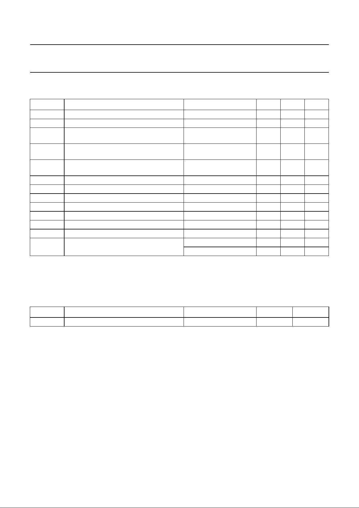
7 LIMITING VALUES
In accordance with the Absolute Maximum Rating System (IEC 134).
SYMBOL PARAMETER CONDITIONS MIN. MAX. UNIT
V
DD
∆V
DD
I
IK
I
OK
I
O
I
, I
DDD
SSD
, I
I
DDA
SSA
I
lu(prot)
P/out power dissipation per output − 100 mW
P
tot
T
stg
T
amb
V
es
DC supply voltage −0.5 +6.5 V
voltage differences between two VDD pins − 550 mV
DC input clamping diode current VI< −0.5 V or
−±10 mA
VI>VDD+ 0.5 V
DC output clamping diode current
(output type 4 mA)
DC output source or sink current
VO< −0.5 V or
−±20 mA
VO>VDD+ 0.5 V
−0.5V<VO<VDD+ 0.5 V −±20 mA
(output type 4 mA)
DC VDD or VSS current per digital supply pin −±100 mA
DC VDD or VSS current per analog supply pin −±50 mA
latch-up protection 100 − mA
total power dissipation − 1.3 W
storage temperature −55 +125 °C
operating ambient temperature −20 +70 °C
electrostatic handling note 1 2000 − V
note 2 200 − V
Notes
1. Human body model: C = 100 pF; R = 1.5 kΩ.
2. Machine model: C = 200 pF; L = 0.75 µH; R = 0 Ω.
8 THERMAL CHARACTERISTICS
SYMBOL PARAMETER CONDITIONS VALUE UNIT
R
th j-a
thermal resistance from junction to ambient in free air 31 K/W
1998 Feb 13 20
Page 21
Philips Semiconductors Preliminary specification
Digital TV Sound Processor (DTVSP) TDA9875
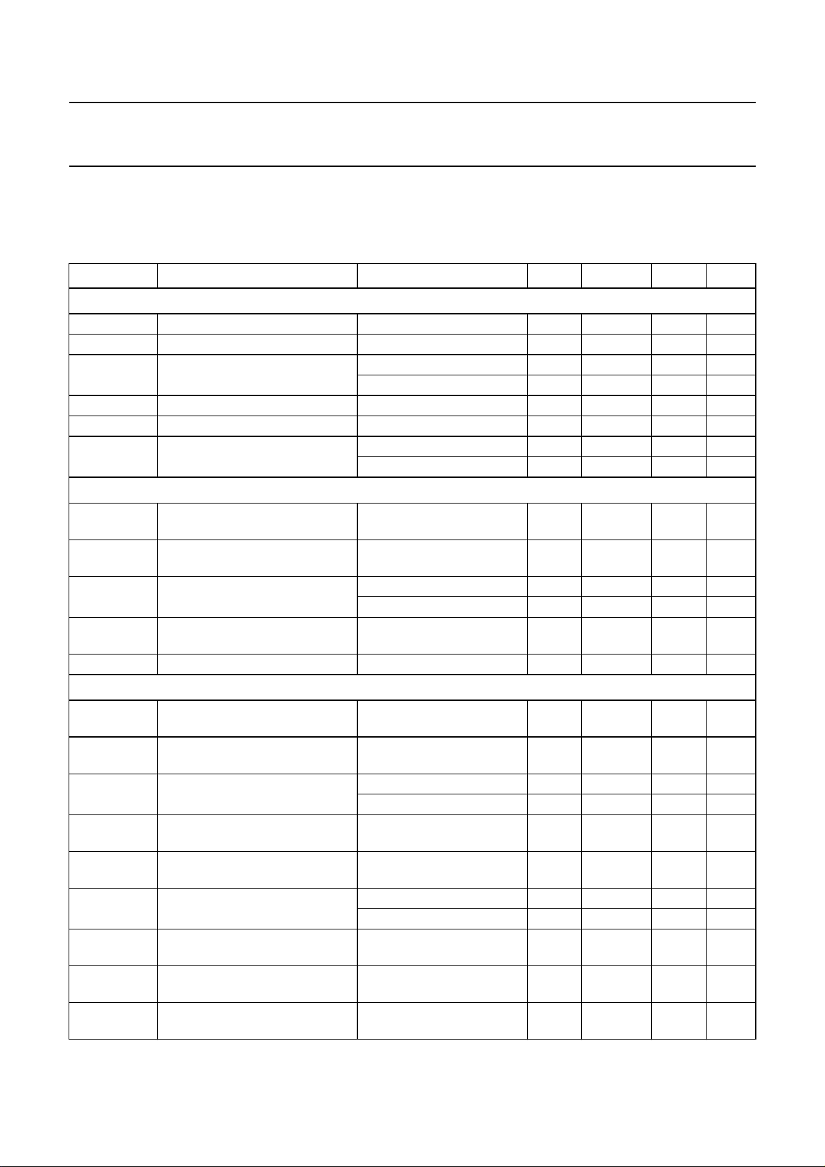
9 CHARACTERISTICS
V
=5V; T
DD
parameters in accordance with system A2; NICAM in accordance with
resistance for AF inputs; unless otherwise specified.
SYMBOL PARAMETER CONDITIONS MIN. TYP. MAX. UNIT
Digital supplies
V
DDD1
V
SSD1
I
DDD1
V
DDD2
V
SSD2
I
DDD2
Demodulator supplies and references
V
DDA1
V
SSA1
I
DDA1
V
ref1
I
ref1(sink)
Audio supplies and references
V
DDA2
V
SSA2
I
DDA2
V
DDA3
V
SSA3
I
DDA3
V
SSA4
V
SSG
V
ref2
=25°C; settings in accordance with B/G standard; FM deviation ±50 kHz; f
amb
“EBU specification”
= 1 kHz; FM sound
mod
; 1 kΩ measurement source
digital supply voltage 1 4.75 5.0 5.5 V
digital supply ground 1 − 0.0 − V
digital supply current 1 V
=5.5V 6580 95mA
DDD1
V
=5.0V 5570 85mA
DDD1
digital supply voltage 2 4.75 5.0 5.5 V
digital supply ground 2 − 0.0 − V
digital supply current 2 V
analog supply voltage for
=5.5V 5065 80mA
DDD2
V
=5.0V 4555 65mA
DDD2
4.75 5.0 5.5 V
demodulator part
analog ground for demodulator
− 0.0 − V
part
analog supply current for
demodulator part
analog reference voltage for
V
=5.5V 2026 31mA
DDA
V
=5.0V 1924 28mA
DDA
referenced to V
DDA1/VSSA1
35 50 65 %
demodulator part
V
sink current 170 220 260 µA
ref1
analog supply voltage for audio
4.75 5.0 5.5 V
ADC part
analog ground for audio ADC
− 0.0 − V
part
analog supply current for audio
ADC part
analog supply voltage for audio
V
= 5.5 V 11 14 17 mA
DDA
V
=5.0V 1013 16mA
DDA
4.75 5.0 5.5 V
DAC part
analog ground for audio DAC
− 0.0 − V
part
analog supply current for audio
DAC part
analog ground for operational
V
= 5.5 V; digital silence 9 12 14 mA
DDA
V
= 5.0 V; digital silence 8 11 13 mA
DDA
− 0.0 − V
amplifier
ground, guard rings for
− 0.0 − V
analog-to-digital circuitry
reference voltage for audio
referenced to V
DDA2/VSSA2
− 50 − %
ADCs
1998 Feb 13 21
Page 22
Philips Semiconductors Preliminary specification
Digital TV Sound Processor (DTVSP) TDA9875
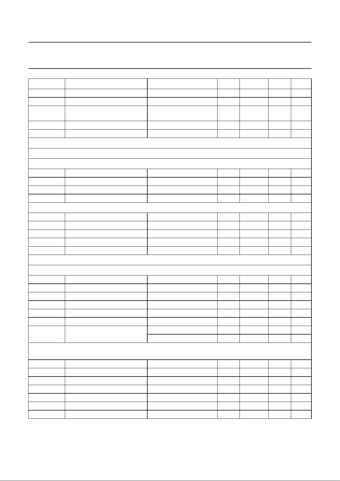
SYMBOL PARAMETER CONDITIONS MIN. TYP. MAX. UNIT
Z
Vref2-VDDA2
Z
Vref2-VSSA2
V
ref3
Z
Vref3-VDDA3
Z
Vref3-VSSA3
Digital inputs and outputs
I
NPUTS
CMOS level input, high drive, pull-down (pins TEST1 and TEST2)
V
IL
V
IH
C
i
Z
i
CMOS level input, hysteresis, high drive, pull-up (pin CRESET)
V
IL
V
IH
V
hys
C
i
Z
i
INPUTS/OUTPUTS
impedance V
impedance V
reference voltage for audio DAC
ref2
ref2
to V
to V
DDA2
SSA2
referenced to V
DDA3/VSSA3
− 20 − kΩ
− 20 − kΩ
− 50 − %
and operational amplifier
impedance V
impedance V
ref3
ref3
to V
to V
DDA3
SSA3
− 20 − kΩ
− 20 − kΩ
LOW level input voltage −− 1.6 V
HIGH level input voltage 3.0 −−V
input capacitance −− 10 pF
input impedance − 50 − kΩ
LOW level input voltage −− 1.6 V
HIGH level input voltage 3.0 −−V
hysteresis voltage − 0.33V
DDD
− V
input capacitance −− 10 pF
input impedance − 50 − kΩ
I2C-bus level input with Schmitt trigger, open-drain output stage (pins SCL and SDA)
V
IL
V
IH
V
HYS
I
LI
C
i
V
OL
C
L
LOW level input voltage −− 1.6 V
HIGH level input voltage 3.0 −−V
hysteresis voltage − 0.33V
DDD
− V
input leakage current −− ±10 µA
input capacitance −− 10 pF
LOW level output voltage −− 0.5 V
load capacitance active pull-up −− 400 pF
passive pull-up −− 200 pF
TTL/CMOS level, high drive, 4 mA 3-state output stage, pull-up (pins PCLK, NICAM, ADDR1, ADDR2, P1, P2, SCK,
WS, SDO1, SDO2, SDI1 and SDI2)
V
IL
V
IH
C
i
V
OL
V
OH
C
L
Z
i
LOW level input voltage −− 0.8 V
HIGH level input voltage 2.0 −−V
input capacitance −− 10 pF
LOW level output voltage IOL=3mA −− 0.5 V
HIGH level output voltage IOH= −3 mA 2.9 −−V
load capacitance active pull-up −− 50 pF
input impedance − 50 − kΩ
1998 Feb 13 22
Page 23
Philips Semiconductors Preliminary specification
Digital TV Sound Processor (DTVSP) TDA9875
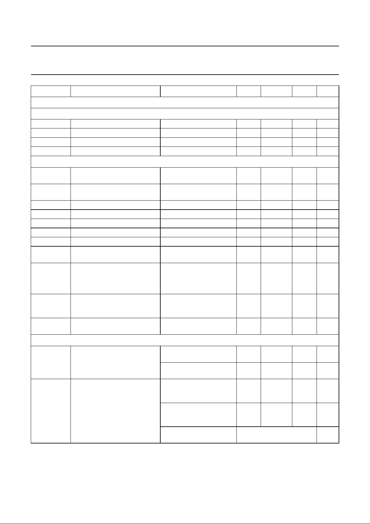
SYMBOL PARAMETER CONDITIONS MIN. TYP. MAX. UNIT
OUTPUTS
4 mA 3-state output stage (pin SYSCLK)
V
OL
V
OH
C
L
I
LIZ
SIF1 and SIF2 analog inputs
V
SIFmax(rms)
V
SIFmin(rms)
AGC AGC range − 21 − dB
f
i
R
i
C
i
∆f
FM
∆f
FM(FS)
C/N
FM
C/N
N
α
ct
LOW level output voltage IOL=2mA −− 0.5 V
HIGH level output voltage IOH= −2 mA 2.9 −−V
load capacitance −− 50 pF
3-state leakage current Vi= 0 to V
maximum composite SIF input
DDD
−− ±10 µA
− 250 − mV
voltage (RMS value)
minimum composite SIF input
− 21 − mV
voltage (RMS value)
input frequency 4 − 9.2 MHz
input resistance 10 13 16 kΩ
input capacitance − 7.5 11 pF
FM deviation B/G standard; THD < 1% 100 −−kHz
FM deviation full-scale level terrestrial FM; level adjust
150 −−kHz
0dB
FM carrier C/Nc ratio NFM bandwidth = 6 MHz;
white noise for
S/N = 40 dB;
“CCIR468”
− 77 −
;
dB
FM
------------- Hz
quasi peak
NICAM carrier C/Nc ratio Nc bandwidth = 6 MHz;
bit error rate = 10−3;
white noise
crosstalk attenuation input
fi= 4 to 9.2 MHz 50 −−dB
− 66 −
dB
----------
Hz
N
channel
Demodulator performance
THD + N total harmonic distortion plus
noise
from FM source to any
output; Vo= 1 V (RMS)
from NICAM source to any
output; V
= 1 V (RMS)
o
S/N signal-to-noise ratio SC1 from FM source to any
output; V
= 1 V (RMS),
o
TIMPOL bit HIGH
SC2 from FM source to any
output; V
= 1 V (RMS),
o
TIMPOL bit HIGH
NICAM source;
= 1 V (RMS)
V
o
1998 Feb 13 23
− 0.3 0.5 %
− 0.1 0.3 %
61 65 − dB
57 60 − dB
NICAM in accordance with
“EBU specification”
; note 2
Page 24

Philips Semiconductors Preliminary specification
Digital TV Sound Processor (DTVSP) TDA9875
SYMBOL PARAMETER CONDITIONS MIN. TYP. MAX. UNIT
B
−3
α
ct
α
cs(stereo)
α
AM
DEP
D
S/N
AM
IDENTIFICATION FOR FM SYSTEMS
mod
p
C/N
p
hys
tun
f
ident
t
ident(on)
t
ident(off)
−3 dB bandwidth from FM source to any
14.5 15 − kHz
output
from NICAM source to any
14.5 15 − kHz
output
crosstalk attenuation from SIF1 or SIF2 to any
65 70 − dB
output
stereo channel separation 40 45 − dB
AM suppression for FM AM: 1 kHz,
50 −−dB
30% modulation; reference:
1 kHz, 50 kHz deviation
de-emphasis 50 µs, 60 µs, 75 µs, J17,
adaptive de-emphasis
AM demodulation SIF level 100 mV (RMS);
− 36 − dB
54% AM; 1 kHz AF;
“CCIR468”
; quasi peak
pilot modulation for identification 25 50 75 %
pilot sideband C/N for
identification start
− 32 −
dB
------ Hz
hysteresis −− 2dB
identification window B/G stereo
slow mode 116.85 − 118.12 Hz
medium mode 116.11 − 118.89 Hz
fast mode 114.65 − 120.46 Hz
B/G dual
slow mode 273.44 − 274.81 Hz
medium mode 272.07 − 276.20 Hz
fast mode 270.73 − 277.60 Hz
total identification time ON slow mode −− 2s
medium mode −− 1s
fast mode −− 0.5 s
total identification time OFF slow mode −− 2s
medium mode −− 1s
fast mode −− 0.5 s
Analog audio inputs
M
ONO INPUT
V
i(nom)(rms)
nominal level input voltage
note 3 − 500 − mV
(RMS value)
V
i(clip)(rms)
clipping level input voltage
THD < 3%; note 4 1250 1400 − mV
(RMS value)
R
i
input resistance note 4 28 35 42 kΩ
1998 Feb 13 24
Page 25
Philips Semiconductors Preliminary specification
Digital TV Sound Processor (DTVSP) TDA9875
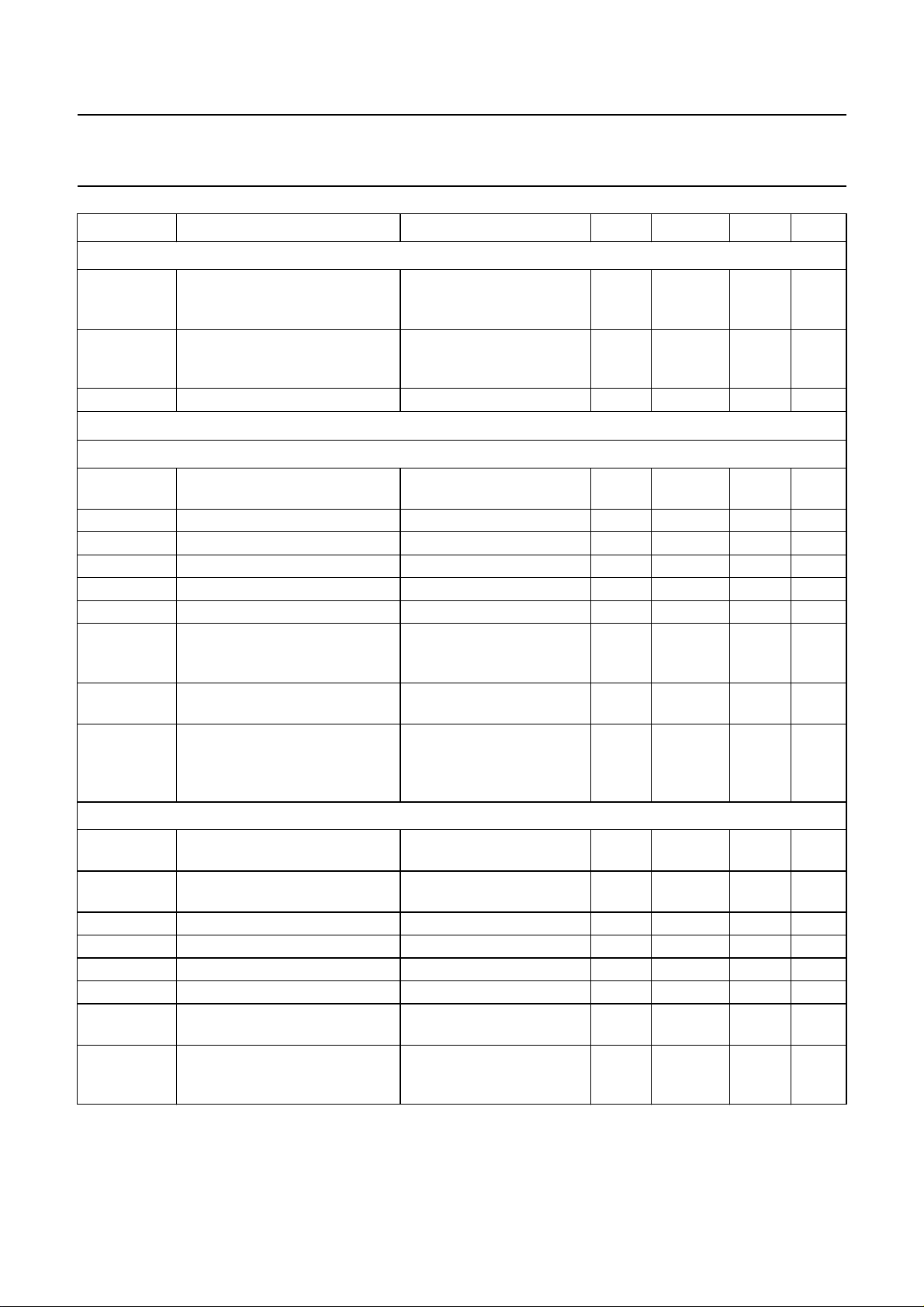
SYMBOL PARAMETER CONDITIONS MIN. TYP. MAX. UNIT
SCART AND EXTERNAL INPUTS
V
i(nom)(rms)
V
i(clip)(rms)
R
i
Analog audio outputs
L
OUDSPEAKER (MAIN) AND HEADPHONE (AUXILIARY) OUTPUTS
V
o(clip)(rms)
R
o
R
L(AC)
R
L(DC)
C
L
V
offset(DC)
α
mute
G
ro(main,aux
PSRR
main,aux
SCART OUTPUTS AND LINE OUTPUT
V
o(nom)(rms)
V
o(clip)(rms)
R
o
R
L(AC)
R
L(DC)
C
L
V
offset(DC)
α
mute
nominal level input voltage at
input pin (RMS value)
−3 dB divider with external
15 kΩ resistor;
− 350 − mV
notes 3 and 5
clipping level input voltage at
input pin (RMS value)
−3 dB divider with external
15 kΩ resistor; THD < 3%;
1250 1400 − mV
notes 4 and 5
input resistance note 4 28 35 42 kΩ
clipping level output voltage
THD < 3% 1400 −−mV
(RMS value)
output resistance 150 250 375 Ω
AC load resistance 10 −−kΩ
DC load resistance 10 −−kΩ
output load capacitance − 10 12 nF
static DC offset voltage − 30 70 mV
mute suppression nominal input signal from
80 −−dB
any source; fi= 1 kHz;
note 3
) roll-off gain at 14.5 kHz for Main
from any source −3 −2 − dB
and Auxiliary channels
power supply ripple rejection for
Main and Auxiliary channels
f
= 70 Hz;
ripple
V
= 100 mV (peak);
ripple
C
=47µF;
Vref
40 45 − dB
signal from I2S-bus
nominal level output voltage
+3 dB amplification; note 3 − 500 − mV
(RMS value)
clipping level output voltage
THD < 3% − 1400 − mV
(RMS value)
output resistance 150 250 375 Ω
AC load resistance 10 −−kΩ
DC load resistance 10 −−kΩ
output load capacitance −− 2.5 nF
static DC offset voltage output amplifiers at +3 dB
− 30 50 mV
position
mute suppression nominal input signal from
80 −−dB
any source; fi= 1 kHz;
note 3
1998 Feb 13 25
Page 26

Philips Semiconductors Preliminary specification
Digital TV Sound Processor (DTVSP) TDA9875
SYMBOL PARAMETER CONDITIONS MIN. TYP. MAX. UNIT
B
line
PSRR
line
Audio performance
THD + N total harmonic distortion plus
S/N signal-to-noise ratio reference voltage
α
ct
α
cs
G
A
line bandwidth from SCART, external,
Auxiliary and mono
sources; −3 dB bandwidth
from DSP sources;
−3 dB bandwidth
power supply ripple rejection f
= 70 Hz;
ripple
V
= 100 mV (peak);
ripple
C
=47µF;
Vref
signal from I2S-bus
noise
V
fi= 1 kHz; bandwidth
i=Vo
= 1 V (RMS);
20 Hz to 15 kHz; note 1
from any analog audio
input to I
from I
2
S-bus
2
S-bus to any
analog audio output
SCART-to-SCART copy − 0.1 0.3 %
SCART-to-Main copy − 0.2 0.5 %
V
= 1.4 V (RMS);
o
fi= 1 kHz;
“CCIR468”
;
quasi peak; note 1
from any analog audio
input to I
from I
2
S-bus
2
S-bus to any
analog audio output
SCART-to-SCART copy 78 90 − dB
SCART-to-Main copy 73 77 − dB
crosstalk attenuation between any analog input
pairs; fi= 1 kHz
between any analog output
pairs; f
=10kHz
i
channel separation between left and right of
any input pair
between left and right of
any output pair
from SCART-to-SCART with
−3 dB input voltage divider
output amplifier in +3 dB
position;
R
=15kΩ±10%
ext
output amplifier in 0 dB
position;
R
=15kΩ±10%
ext
from external input to
=15kΩ±10%; note 1 −1.5 0 +1.5 dB
R
ext
loudspeaker
20 −−kHz
14.5 −−kHz
40 45 − dB
− 0.1 0.3 %
− 0.1 0.3 %
73 77 − dB
78 90 − dB
70 −−dB
65 −−dB
65 −−dB
60 −−dB
−1.5 0 +1.1 dB
−4.5 −3.0 −1.9 dB
1998 Feb 13 26
Page 27
Philips Semiconductors Preliminary specification
Digital TV Sound Processor (DTVSP) TDA9875
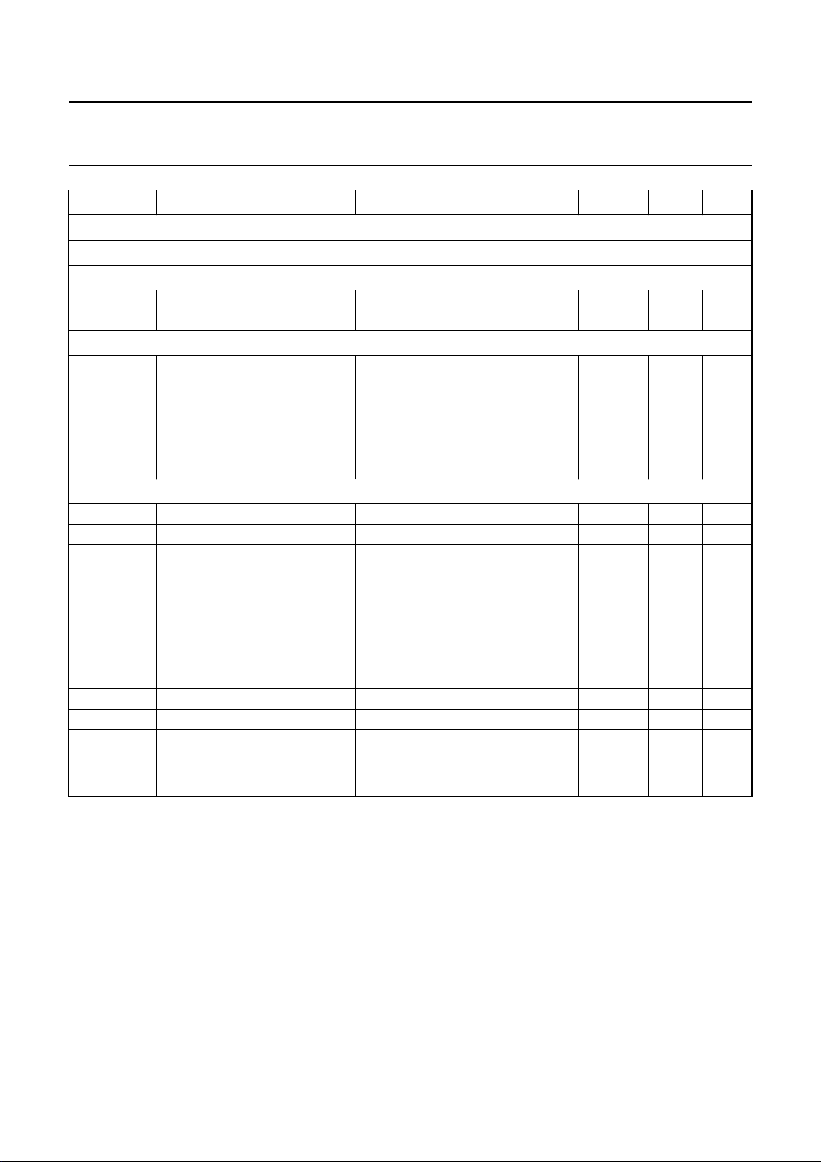
SYMBOL PARAMETER CONDITIONS MIN. TYP. MAX. UNIT
VCXO and clock generation
VCXO
Crystal input
C
i
V
bias(DC)
Crystal output
V
osc(p-p)
V
bias(DC)
G
m
C
o
CRYSTAL SPECIFICATION (FUNDAMENTAL MODE)
f
xtal
C
L
C
1
C
0
Φ
pull
R
R
R
N
∆T temperature range −20 +25 +70 °C
X
J
X
D
X
A
input capacitance −− 10 pF
DC bias voltage Ri= 100 kΩ 3.5 3.63 3.7 V
oscillation amplitude
− 1.4 − V
(peak-to-peak value)
DC bias voltage 2.0 2.4 2.8 V
mutual conductance at
24.576 MHz
16.6 17.6 18.8
mA
---------
V
output capacitance −− 10 pF
crystal frequency − 24.576 − MHz
load capacitance − 20 − pF
series capacitance − 20 − fF
parallel capacitance −− 7pF
pulling sensitivity CL changed from
18 to 16 pF
− 25 −
10
----------pF
6–
equivalent series resistance at nominal frequency −− 30 Ω
equivalent series resistance of
2R
−−Ω
R
unwanted mode
adjustment tolerance −− ±30 10
drift across temperature range −− ±30 10
ageing −− ±5
−6
−6
10
-----------
year
6–
1998 Feb 13 27
Page 28

Philips Semiconductors Preliminary specification
Digital TV Sound Processor (DTVSP) TDA9875
Notes to the characteristics
1. ADC level adjust = +6 dB, all other level adjusts = 0 dB, if external −3 dB divider is used set output buffer gain to
+3 dB, tone control to 0 dB, AVL off and volume control to 0 dB.
2. Due to companding, the quantization noise of the NICAM system limits signal-to-noise ratio to 62 dB
(unweighted; RMS value).
3. Definition of nominal levels:
The full-scale level for analog audio signals is VFS= 1.4 V (RMS). The nominal level at the digital crossbar switch is
defined at −15 dB (full-scale).
a) Audio input nominal levels:
SCART: 350 mV (at pin); −12 dB (full-scale)
external, mono: 500 mV; −9 dB (full-scale)
b) FM/AM path nominal (maximum) levels:
system M: 15 kHz deviation; −23.7 dB (full-scale)
system B/G, D/K, I: 27 kHz deviation; −18.6 dB (full-scale)
SAT stereo (maximum): 50 kHz deviation; −13.3 dB (full-scale)
SAT mono (maximum): 85 kHz deviation; −8.7 dB (full-scale)
AM: 54% modulation; full-scale SIF ADC; −20 dB (full-scale)
c) NICAM path nominal (maximum) levels:
system B/G: −18.2 dB (full-scale)
system I: −22.8 dB (full-scale)
maximum level: 0.0 dB (full-scale).
4. If the supply voltage for the TDA9875 is switched off, because of the ESD protection circuitry, all audio input pins are
short-circuited. To avoid a short-circuit at the SCART inputs a 15 kΩ resistor (−3 dB divider) has to be used.
5. The SCART specification allows a signal level of up to 2 V (RMS). Because of signal handling limitations due to the
5 V supply voltage for the TDA9875, there is a need for fixed 3 dB attenuators at the SCART inputs. To achieve
SCART-to-SCART copies with 0 dB gain, there are +3 dB/0 dB amplifiers at the outputs of SCART 1 and SCART 2
and at the line output. The attenuator is realized by an internal resistor that works together with an external series
resistor as a voltage divider. With this voltage divider the maximum SCART input signal level of 2 V (RMS) is scaled
down to 1.4 V (RMS) at the input pin. To avoid clipping, the +3 dB gain must not be used if the SCART input signal
is larger than 1.4 V (RMS).
1998 Feb 13 28
Page 29

Philips Semiconductors Preliminary specification
Digital TV Sound Processor (DTVSP) TDA9875
10 I2C-BUS CONTROL
10.1 Introduction
2
The TDA9875 is fully controlled via the I
C-bus. Control is
exercised by writing data to one or more internal registers.
Status information can be read from an array of registers
to enable the controlling microcontroller determine
whether any action is required.
The device has an I2C-bus slave transceiver, in
accordance with the fast-mode specification, with a
maximum speed of 400 kbits/s. Information concerning the
I2C-bus can be found in brochure
it”
(order number 9398 393 40011). To avoid conflicts in a
“I2C-bus and how to use
real application with other ICs providing similar or
complementary functions, there are four possible slave
addresses available which can be selected by pins
ADDR1 and ADDR2 (see Table 7).
Table 7 Possible slave addresses
ADDR2 ADDR1 SLAVE ADDRESS A6 TO A0
0 0 1 0 1 1 0 0 0
0 1 1 0 1 1 0 0 1
1 0 1 0 1 1 0 1 0
1 1 1 0 1 1 0 1 1
2
The I
C-bus interface remains operational in the standby
mode of the TDA9875 to allow control of the analog source
selectors with regard to SCART-to-SCART copying.
The device will not respond to a ‘general call’ on the
I2C-bus, i.e. when a slave address of 0000000 is sent by a
master.
The data transmission between the microcontroller and
the other I2C-bus controlled ICs is not disturbed when the
supply voltage of the TDA9875 is not connected.
10.2 Power-up state
At power-up the device is in the following state:
• All outputs muted
• No sound carrier frequency loaded
• General-purpose I/O pins ready for input (HIGH)
• Input SIF1 selected with:
– AGC on
– Small hysteresis.
• Demodulators for both sound carriers set to FM with:
– Identification for B/G, D/K, response time 1 s
– Level adjust set to 0 dB
– De-emphasis 50 µs
– Matrix set to mono.
• Main channel set to FM input with:
– Spatial off
– Pseudo off
– AVL off
– Volume mute
– Bass flat
– Treble flat
– Contour off
– Bass boost flat.
• Auxiliary channel set to FM input with:
– Volume mute
– Bass flat
– Treble flat.
• Feature interface all outputs off
• Beeper off
• Monitoring of carrier 1 FM demodulator DC output.
After power-up a device initialization has to be performed
2
via the I
C-bus to put the TDA9875 into the proper mode
of operation, in accordance with the desired TV standard,
audio control settings, etc.
1998 Feb 13 29
Page 30
Philips Semiconductors Preliminary specification
Digital TV Sound Processor (DTVSP) TDA9875
10.3 Slave receiver mode
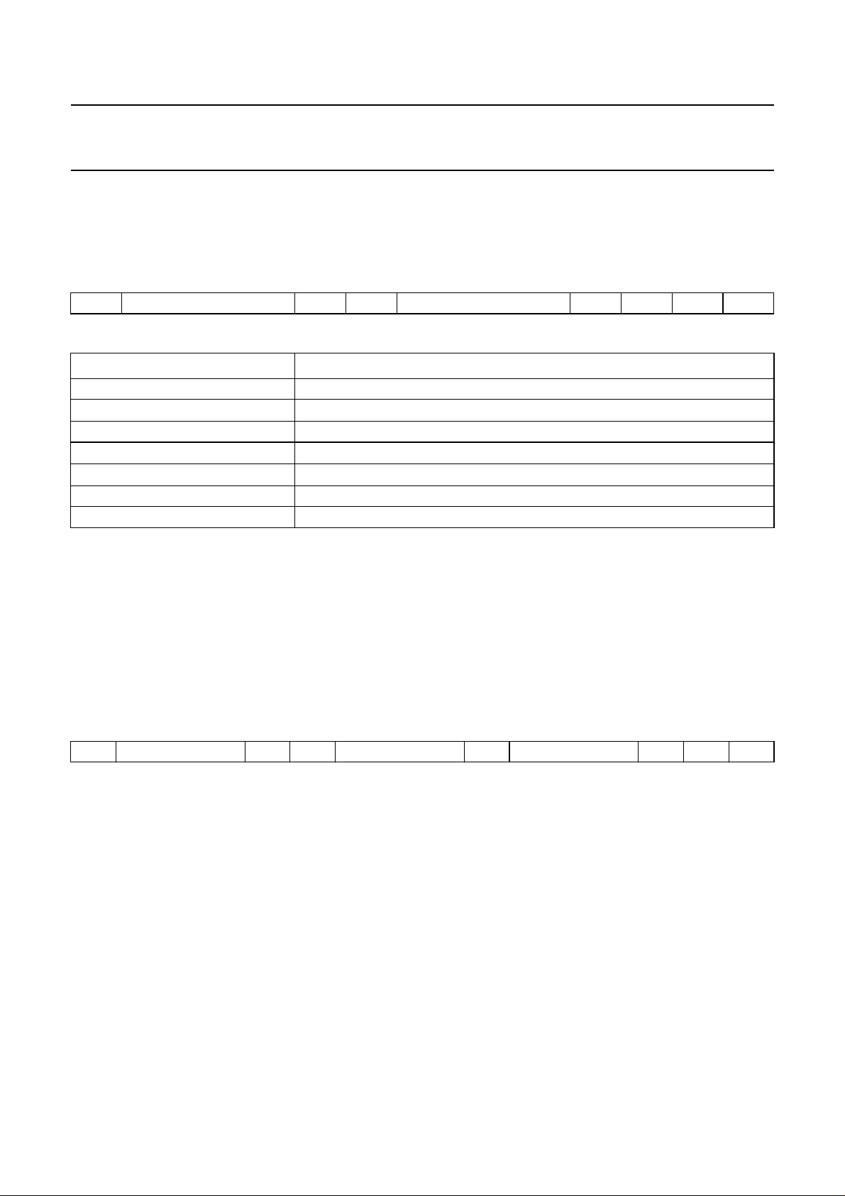
As a slave receiver, the TDA9875 provides 46 registers for storing commands and data. These registers are accessed
via so-called subaddresses. A subaddress can be thought of as a pointer to an internal memory location.
2
Table 8 I
S SLAVE ADDRESS 0 ACK SUBADDRESS ACK DATA ACK P
Table 9 Explanation of Table 8
S START condition
SLAVE ADDRESS
0 data direction bit (write to device)
ACK
SUBADDRESS
DATA data byte to be written into register
P STOP condition
C-bus; slave address, subaddress and data format
BIT FUNCTION
7-bit device address
acknowledge
address of register to write to
It is allowed to send more than one data byte per transmission to the TDA9875. In this event, the subaddress is
automatically incremented after each data byte, resulting in storing the sequence of data bytes at successive register
locations, starting at SUBADDRESS. A transmission can start at any valid subaddress. Each byte is acknowledged with
ACK (acknowledge).
There is no ‘wrap-around’ of subaddresses.
Commands and data are processed as soon as they have been completely received. Functions requiring more than one
byte will, thus, be executed only after all bytes for that function have been received. Should the transmission is terminated
(STOP condition) before all bytes have been received, the incomplete data for that function are ignored.
Table 10 Format for a transmission employing auto-increment of subaddresses
S SLAVE ADDRESS 0 ACK SUBADDRESS ACK DATA BYTE A
Note
1. n data bytes with auto-increment of subaddresses.
Data patterns sent to the various subaddresses are not checked for being illegal or not at that address, except for the
functions of volume, bass, treble control, bass boost and level adjust.
Detection of a STOP condition without a preceding acknowledge bit is regarded as a bus error. The last operation will
not then be executed.
(1)
DATA ACK P
1998 Feb 13 30
Page 31
Philips Semiconductors Preliminary specification
Digital TV Sound Processor (DTVSP) TDA9875
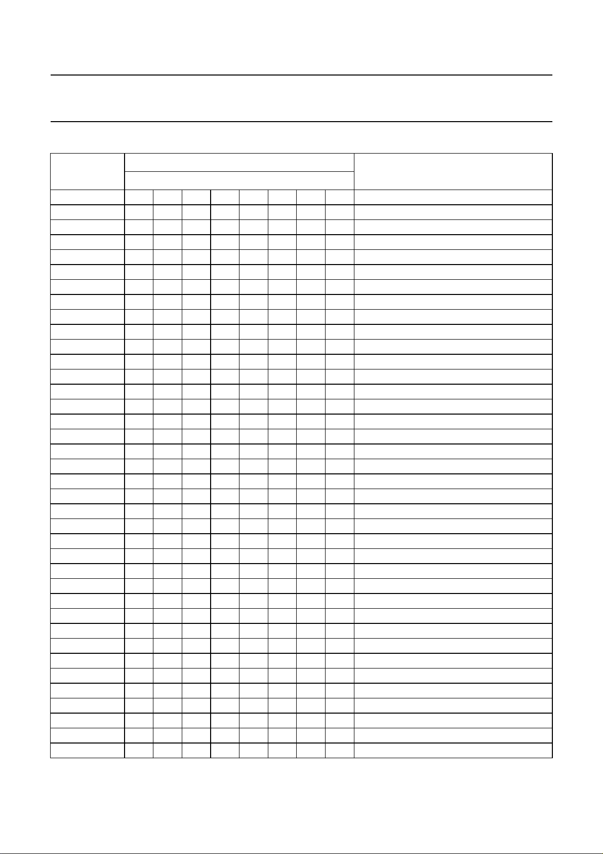
Table 11 Overview of the slave receiver registers (note 1)
SUBADDRESS
(DECIMAL)
0 XXXgggggAGC gain selection (ignored, if AGC off)
1 ccccccccgeneral configuration
2 p X X m m s s s monitor select, peak detector on/off
3 ffffffffcarrier 1 frequency; MS part
4 ffffffffcarrier 1 frequency
5 ffffffffcarrier 1 frequency; LS part
6 ffffffffcarrier 2 frequency; MS part
7 ffffffffcarrier 2 frequency
8 ffffffffcarrier 2 frequency; LS part
9 cccXccccdemodulator configuration
10 ddddddddFM de-emphasis
11 XXXXXmmmFM matrix
12 XXXlllllchannel 1 output level adjust
13 XXXlllllchannel 2 output level adjust
14 X X c c X X c c NICAM configuration
15 XXXlllllNICAM output level adjust
16 llllllllNICAM lower error limit
17 uuuuuuuuNICAM upper error limit
18 mmmmmmmmaudio mute control
19 g m m m g s s s DAC output select
20 X g m m X s s s SCART 1 output select
21 X g m m X s s s SCART 2 output select
22 X g m m X X X s line output select
23 ssslllllADC output select
24 X m m m X s s s Main channel select
25 XXssppaaaudio effects (AVL, pseudo, spatial)
26 vvvvvvvvvolume control, Main left
27 vvvvvvvvvolume control, Main right
28 XXXccccccontour control, Main
29 XXXbbbbbbass control, Main
30 XXXttttttreble control, Main
31 X m m m X s s s Auxiliary channel select
32 vvvvvvvvvolume control, Auxiliary left
33 vvvvvvvvvolume control, Auxiliary right
34 XXXbbbbbbass control, Auxiliary
35 XXXttttttreble control, Auxiliary
36 XXXcccccfeature interface configuration
37 XmmmX s s sI
MSB LSB
DATA
2
S1 output select
FUNCTION
1998 Feb 13 31
Page 32
Philips Semiconductors Preliminary specification
Digital TV Sound Processor (DTVSP) TDA9875
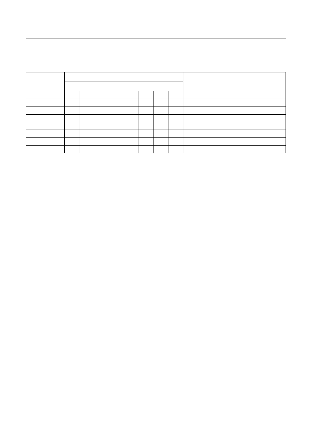
SUBADDRESS
(DECIMAL)
MSB LSB
38 XXXiiiiiI
39 XXXoooooI
40 XmmmX s s sI
41 XXXiiiiiI
42 XXXoooooI
DATA
FUNCTION
2
S1 input level adjust
2
S1 output level adjust
2
S2 output select
2
S2 input level adjust
2
S2 output level adjust
43 XXXXX f f fbeeper frequency
44 XXvvvvvvbeeper volume, Main and Auxiliary
45 bbbbbbbbbass boost, Main left and right
Note
1. X indicates bits that have not yet been assigned to a function. Their meaning is ‘don’t care’. They should be written
as a zero.
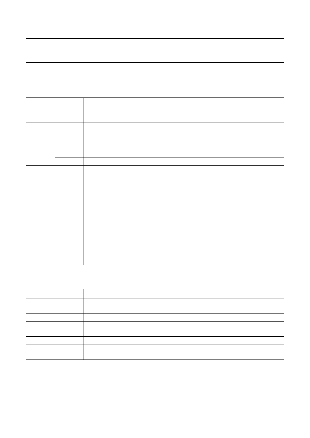
The following sub-sections provide a detailed description of the slave receiver registers:
10.3.1 AGC
GAIN REGISTER
10.3.1.1 Description
If the automatic gain control function is switched off in the General Configuration Register, the contents of this register
will define a fixed gain of the AGC stage. The input voltages given are meant to generate a full-scale output from the SIF
ADC. If automatic gain control is on, the contents of this register is ignored.
It should be noted that the input voltages should be considered as approximate target values.
1998 Feb 13 32
Page 33

Philips Semiconductors Preliminary specification
Digital TV Sound Processor (DTVSP) TDA9875
10.3.1.2 Definition
Table 12 Subaddress 0 (notes 1 and 2)
MSB LSB
B7 B6 B5 B4 B3 B2 B1 B0
XXX11111 240
XXX11110 214
XXX11101 195
XXX11100 176
XXX11011 159
XXX11010 145
XXX11001 131
XXX11000 119
XXX10111 107
XXX10110 99
XXX10101 90
XXX10100 82
XXX10011 76
XXX10010 70
XXX10001 65
XXX10000 60
XXX01111 55
XXX01110 51
XXX01101 48
XXX01100 45
XXX01011 42
XXX01010 39
XXX01001 36
XXX01000 34
XXX00111 32
XXX00110 30
XXX00101 29
XXX00100 27
XXX00011 25
XXX00010 24
XXX00001 23
XXX00000 22
SIF INPUT VOLTAGE
[mV (RMS)]
Notes
1. X = don’t care.
2. The default setting at power-up is 00000000.
1998 Feb 13 33
Page 34
Philips Semiconductors Preliminary specification
Digital TV Sound Processor (DTVSP) TDA9875
10.3.2 GENERAL CONFIGURATION REGISTER
10.3.2.1 Description
Table 13 Description of Table 14
NAME HIGH/LOW FUNCTION
SIFSEL HIGH Selects pin SIF2 for input (recommended for satellite tuner).
LOW Pin SIF1 (terrestrial TV) is selected.
AGCOFF HIGH Forces the AGC block to a fixed gain as defined in the AGC gain register.
LOW The automatic gain control function is enabled and the contents of the AGC gain register is
ignored.
AGCSLOW HIGH A longer decay time and larger hysteresis are selected for input signals with strong video
modulation (intercarrier). This bit only has an effect when bit AGCOFF = 0.
LOW Selects normal attack and decay times for the AGC and a small hysteresis.
INIT HIGH Causes initialization of TDA9875 to its default settings. This has the same effect as a
power-on reset. If there is a conflict between the default settings and any bit set HIGH in
this register, the bits of this register have priority over the corresponding default setting.
LOW This bit is automatically reset to LOW after initialization. When set LOW, the TDA9875 is in
its normal mode of operation.
STDBY HIGH Puts the TDA9875 into the standby mode. Most functions are disabled and power
dissipation is somewhat reduced, but the analog selectors/matrices remain operational to
support analog copying from SCART 1 to SCART 2 and vice versa.
LOW The TDA9875 is in its normal mode of operation. On return from standby mode, the device
is in its power-on reset mode and needs to be re-initialized.
P1OUT,
P2OUT
− These bits control the general purpose input/output pins. The contents of these bits is
written directly to the corresponding pins. If input is desired, the bits must be set HIGH to
allow the pins to be pulled LOW externally. Input from the pins is reflected in the device
status register (see Section 10.4, subaddress 0). P1OUT is recommended to be used for
switching an SIF trap for the adjacent picture carrier in designs that employ such a trap.
10.3.2.2 Definition
Table 14 Subaddress 1 (note 1)
BIT NAME DESCRIPTION
7 (MSB) P2OUT general purpose I/O pin 2
6 P1OUT general purpose I/O pin 1
5 STDBY stand-by mode on/off
4 INIT initialize to defaults (as reset)
3 X don’t care
2 AGCSLOW AGC decay time
1 AGCOFF AGC on/off
0 (LSB) SIFSEL SIF input select
Note
1. The default setting at power-up is 11000000.
1998 Feb 13 34
Page 35
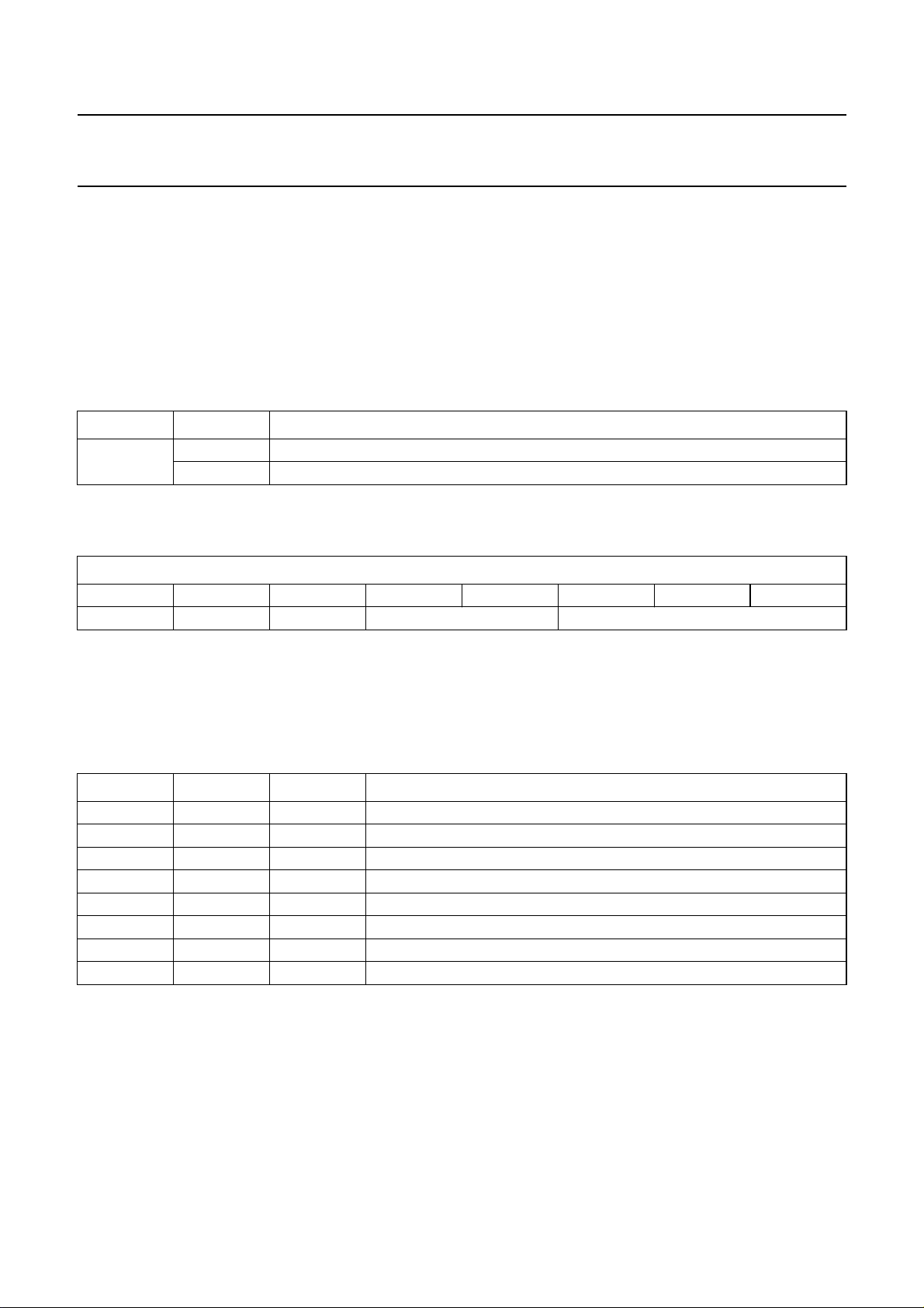
Philips Semiconductors Preliminary specification
Digital TV Sound Processor (DTVSP) TDA9875
10.3.3 MONITOR SELECT REGISTER
10.3.3.1 Description
This register is used to define the signal source, the level of which is to be monitored, and if the peak level is to be
monitored. Peak level refers to the magnitude of the maximum excursion of a signal. Data can be read-out in the I2C-bus
slave transmitter mode (see Section 10.4, subaddresses 5 and 6).
Audio magnitude/phase is related to the FM demodulator output. Phase information is provided, when it operates in
FM mode, while magnitude is supplied in AM mode.
Table 15 Description of bit PEAKMON
NAME HIGH/LOW FUNCTION
PEAKMON HIGH selects the peak level of a source to be monitored
LOW the last sample will be supplied
10.3.3.2 Definition
Table 16 Subaddress 2 (notes 1, 2 and 3)
MSB LSB
B7 B6 B5 B4 B3 B2 B1 B0
PEAKMON X X see Table 18 see Table 17
Notes
1. X = don’t care.
2. PEAKMON is described in Section 10.3.3.1.
3. The default setting at power-up is 00000000.
Table 17 Signal source (note 1)
B2 B1 B0 SIGNAL SOURCE
0 0 0 DC output of FM demodulator
0 0 1 audio magnitude/phase, FM demodulator output
0 1 0 crossbar input from FM/AM channel
0 1 1 crossbar input from NICAM channel
1 0 0 crossbar input from I
1 0 1 crossbar input from I
1 1 0 crossbar input from audio ADC channel
1 1 1 input to Main channel DAC (without beeper)
Note
1. The term ‘crossbar’ refers to the digital selector, where level-adjusted signals from various sources are available.
2
S1 channel
2
S2 channel
1998 Feb 13 35
Page 36

Philips Semiconductors Preliminary specification
Digital TV Sound Processor (DTVSP) TDA9875
Table 18 Monitor output
B4 B3 MONITOR OUTPUT
00
L input R input+
------------------------------------------2
0 1 L input (channel 1, respectively)
1 0 R input (channel 2, respectively)
10.3.3.3 Note
By reading out Level Read-out Registers (subaddresses
5 and 6, see Section 10.4), the current peak level will be
reset.
10.3.4 C
ARRIER 1 FREQUENCY REGISTER
10.3.4.1 Description
The three bytes together constitute a 24-bit frequency
control word to represent the sound carrier (i.e. mixer)
frequency in accordance with the following formula:
data
f
---------
mix
f
clk
24
2
×=
Where:
Data = 24-bit frequency control word
f
= desired sound carrier frequency
mix
f
= 12.288 MHz (clock frequency of mixer)
clk
224= 16777216 (number of steps in a 24-bit word size).
Example: A 5.5 MHz sound carrier frequency will be
generated by sending the following sequence of data
bytes to the TDA9875 (data = 7509333 in decimal notation
or 729555 in hex): 01110010 10010101 01010101.
As three bytes are required to define a carrier frequency,
execution of this command starts only after all bytes have
been received. If an error occurs, e.g. a premature STOP
condition, partial data for this function is ignored.
The default setting at power-up is 00000000 for all three
bytes.
Table 19 Subaddresses 3 to 5
BIT SUBADDRESSES
7 (MSB)
6
5
4
3
3
2
1
0
7
6
5
4
3
4
2
1
0
7
6
5
4
3
5
2
1
0 (LSB)
10.3.5 C
ARRIER 2 FREQUENCY REGISTER
10.3.5.1 Description
Same as for sound carrier 1.
If the carrier 2 frequency register is used, it will be for either
the second FM sound carrier of a terrestrial or satellite FM
program or the NICAM sound carrier.
10.3.4.2 Definition
Most significant part at subaddress 3.
1998 Feb 13 36
10.3.5.2 Definition
Subaddresses 6 to 8.
Same as for sound carrier 1, except for subaddresses
used.
Page 37
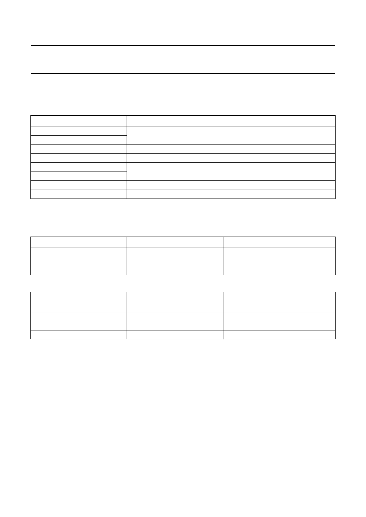
Philips Semiconductors Preliminary specification
Digital TV Sound Processor (DTVSP) TDA9875
10.3.6 DEMODULATOR CONFIGURATION REGISTER
10.3.6.1 Definition
Table 20 Subaddress 9 (note 1; see Table 23)
BIT NAME DESCRIPTION
7 (MSB) IDMOD1 response time for FM sound mode identification
6 IDMOD0
5 IDAREA application area for FM identification
4 X don’t care
3 CH2MOD1 channel 2 receive mode
2 CH2MOD0
1 CH1WIDE channel 1 bandwidth
0 (LSB) CH1MODE channel 1 receive mode
Note
1. The default setting at power-up is 00000000.
Table 21 Channel 2 receive mode (see Table 20)
B3 B2 CHANNEL 2
00 FM
01 AM
1 0 NICAM
Table 22 Identification mode (see Table 20)
B7 B6 IDENT MODE
0 0 slow
0 1 medium
1 0 fast
1 1 off/reset
1998 Feb 13 37
Page 38
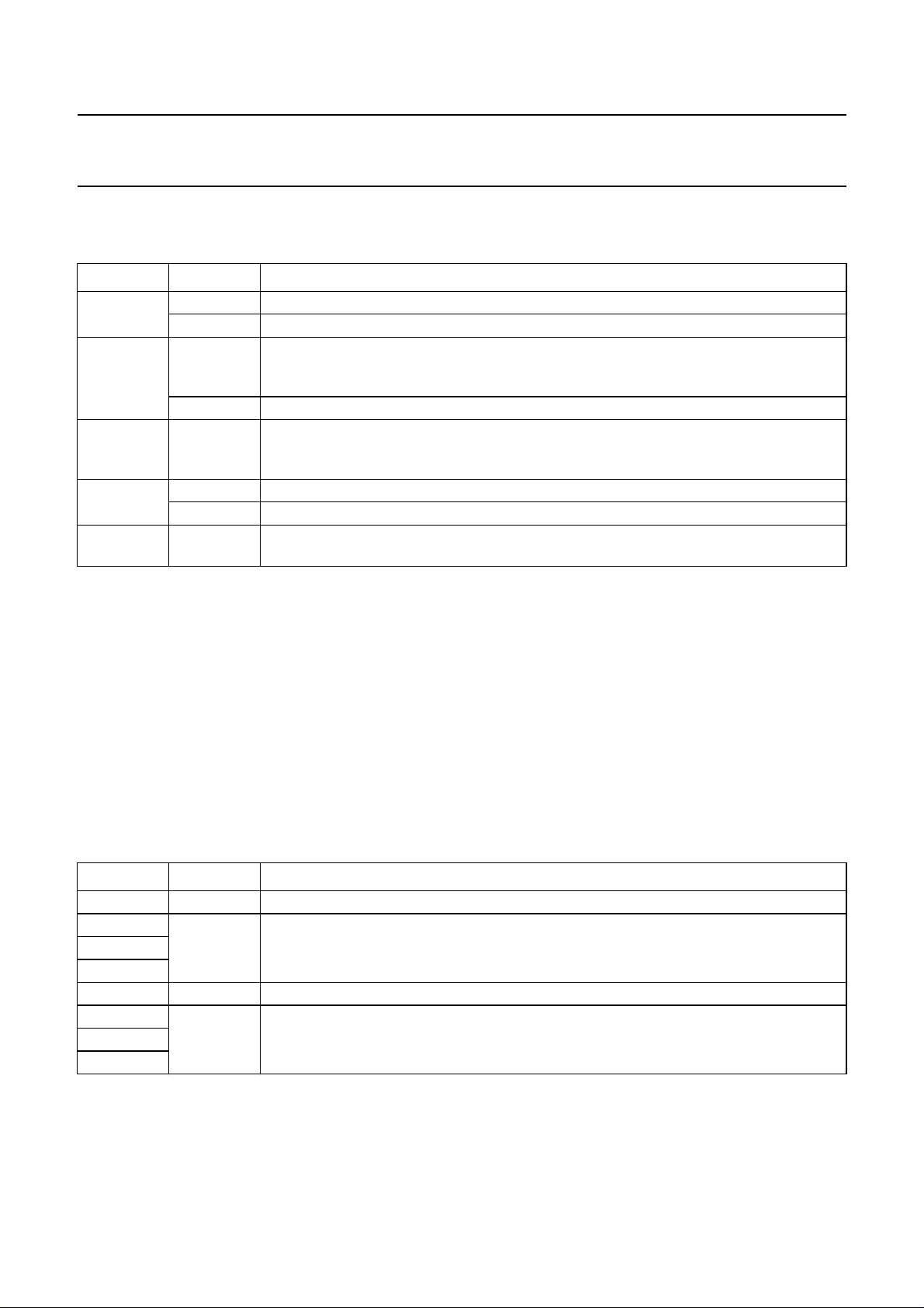
Philips Semiconductors Preliminary specification
Digital TV Sound Processor (DTVSP) TDA9875
10.3.6.2 Description
Table 23 Description of subaddress 9 (notes 1 and 2)
NAME HIGH/LOW FUNCTION
CH1MODE HIGH Selects the hardware for the first sound carrier to operate in AM mode.
LOW FM mode is assumed. This applies to both terrestrial and satellite FM reception.
CH1WIDE HIGH Switches the decimation filters for the first sound carrier to a wide bandwidth, so that the
main sound carrier of a satellite channel with its larger deviation can be handled without
additional distortion.
LOW The bandwidth is narrow to cope with the intermodulation requirements of FM stereo.
CH2MOD0,
CH2MOD1
IDAREA HIGH Selects FM identification frequencies in accordance with the specification for Korea.
IDMOD0,
IDMOD1
− These bits control the hardware for the second sound carrier in accordance with the
truth Table 21. The NICAM mode employs a wider bandwidth of the decimation filters
than the FM mode.
LOW Frequencies for Europe are selected (B/G and D/K standard).
− These bits define the response time after which a sound mode identification result may
be expected. The longer the time, the more reliable the identification.
Notes
1. It is recommended to switch the FM sound mode identification off whenever the received program is not a terrestrial
2-carrier sound.
2. Switching the identification off will reset the associated hardware to a defined state.
10.3.7 FM
DE-EMPHASIS REGISTER
10.3.7.1 Description
This register is used to select the proper de-emphasis characteristics as appropriate for the standard of the received
carrier. Bits B3 to B0 apply to sound carrier 1, bits B7 to B4 apply to sound carrier 2. In the event of FM stereo reception,
both groups must be set to the same characteristics.
10.3.7.2 Definition
Table 24 Subaddress 10 (note 1)
BIT NAME DESCRIPTION
7 (MSB) ADEEM2 adaptive de-emphasis on/off
6 time constant selection for FM de-emphasis
5
4
3 ADEEM1 adaptive de-emphasis on/off
2 time constant selection for FM de-emphasis
1
0 (LSB)
Note
1. The default setting at power-up is 00000000.
1998 Feb 13 38
Page 39
Philips Semiconductors Preliminary specification
Digital TV Sound Processor (DTVSP) TDA9875
Table 25 De-emphasis
B6 and B2 B5 and B1 B4 and B0 DE-EMPHASIS
00050µs (Europe)
00160µs
01075µs (M standard)
011J17
100off
Table 26 Description of bits ADEEM1 and ADEEM2 (note 1)
NAME HIGH/LOW FUNCTION
ADEEM1,
ADEEM2
Note
1. The FM de-emphasis gain is 0 dB at 40 Hz.
HIGH Activates the adaptive de-emphasis function, which is required for certain satellite
FM channels. The standard FM de-emphasis must then be set to 75 µs.
LOW The adaptive de-emphasis is off.
10.3.8 FM
MATRIX REGISTER
10.3.8.1 Description
This register is used to select the proper dematrixing characteristics as appropriate for the standard of the received
carrier and the related sound mode identification. For the dematrixing, it is assumed that the output from sound carrier 1
is on channel L input.
10.3.8.2 Definition
Table 27 Subaddress 11 (notes 1 and 2)
MSB LSB
B7 B6 B5 B4 B3 B2 B1 B0
X X X X X see Table 28
Notes
1. X = don’t care.
2. The default setting at power-up is 00000000.
Table 28 Description of Subaddress 11 (bits B2 to B0)
B2 B1 B0 L OUTPUT R OUTPUT MODE
0 0 0 L input L input mono 1
0 0 1 R input R input mono 2
0 1 0 L input R input dual
0 1 1 R input L input dual swapped
100
101
2L input − R input R input
L input R input+
-------------------------------------------
L input R input–
2
------------------------------------------ 2
stereo Europe
stereo Korea
1998 Feb 13 39
Page 40
Philips Semiconductors Preliminary specification
Digital TV Sound Processor (DTVSP) TDA9875
10.3.9 CHANNEL 1 OUTPUT LEVEL ADJUST REGISTER
10.3.9.1 Description
This register is used to correct for standard and station-dependent differences of signal levels. Table 29 applies to sound
carrier 1.
10.3.9.2 Definition
Table 29 Subaddress 12 (notes 1 and 2)
MSB LSB
B7 B6 B5 B4 B3 B2 B1 B0
XXX01111 +15
XXX01110 +14
XXX01101 +13
XXX01100 +12
XXX01011 +11
XXX01010 +10
XXX01001 +9
XXX01000 +8
XXX00111 +7
XXX00110 +6
XXX00101 +5
XXX00100 +4
XXX00011 +3
XXX00010 +2
XXX00001 +1
XXX00000 0
XXX11111 −1
XXX11110 −2
XXX11101 −3
XXX11100 −4
XXX11011 −5
XXX11010 −6
XXX11001 −7
XXX11000 −8
XXX10111 −9
XXX10110 −10
XXX10101 −11
XXX10100 −12
XXX10011 −13
XXX10010 −14
XXX10001 −15
X X X 1 0 0 0 0 mute
GAIN SETTING
(dB)
Notes
1. X = don’t care.
2. The default setting at power-up is 00000000.
1998 Feb 13 40
Page 41
Philips Semiconductors Preliminary specification
Digital TV Sound Processor (DTVSP) TDA9875
10.3.10 CHANNEL 2 OUTPUT LEVEL ADJUST REGISTER
10.3.10.1 Description
This register is used to correct for standard and station-dependent differences of signal levels. Table 30 applies to sound
carrier 2 in its FM and AM modes. In the event of FM stereo or FM dual language reception, channels 1 and 2 should be
adjusted to the same level.
10.3.10.2 Definition
Table 30 Subaddress 13 (notes 1 and 2)
MSB LSB
B7 B6 B5 B4 B3 B2 B1 B0
XXX01111 +15
XXX01110 +14
XXX01101 +13
XXX01100 +12
XXX01011 +11
XXX01010 +10
XXX01001 +9
XXX01000 +8
XXX00111 +7
XXX00110 +6
XXX00101 +5
XXX00100 +4
XXX00011 +3
XXX00010 +2
XXX00001 +1
XXX00000 0
XXX11111 −1
XXX11110 −2
XXX11101 −3
XXX11100 −4
XXX11011 −5
XXX11010 −6
XXX11001 −7
XXX11000 −8
XXX10111 −9
XXX10110 −10
XXX10101 −11
XXX10100 −12
XXX10011 −13
GAIN SETTING
(dB)
1998 Feb 13 41
Page 42
Philips Semiconductors Preliminary specification
Digital TV Sound Processor (DTVSP) TDA9875
MSB LSB
B7 B6 B5 B4 B3 B2 B1 B0
XXX10010 −14
XXX10001 −15
X X X 1 0 0 0 0 mute
Notes
1. X = don’t care.
2. The default setting at power-up is 00000000.
10.3.11 NICAM
CONFIGURATION REGISTER
10.3.11.1 Definition
Table 31 Subaddress 14 (note 1)
BIT NAME DESCRIPTION
7 (MSB) X don’t care
6 X don’t care
5 TIMPOL timing loop polarity
4 DOUTEN data output enable
3 X don’t care
2 X don’t care
1 NDEEM de-emphasis on/off
0 (LSB) AMUTE auto-muting on/off
GAIN SETTING
(dB)
Note
1. The default setting at power-up is 00000000.
1998 Feb 13 42
Page 43
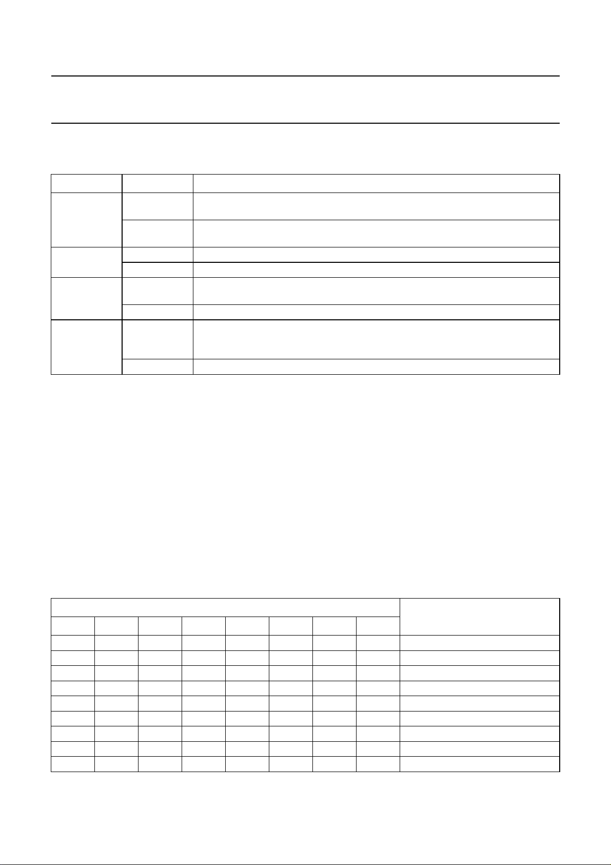
Philips Semiconductors Preliminary specification
Digital TV Sound Processor (DTVSP) TDA9875
10.3.11.2 Description
Table 32 Description of Table 31 (notes 1, 2 and 3)
NAME HIGH/LOW FUNCTION
AMUTE HIGH Automatic muting is disabled. This bit has only an effect when the second sound
carrier is set to NICAM.
LOW enables the automatic switching between NICAM and the program on the first sound
carrier (i.e. FM mono or AM), dependent on the NICAM bit error rate
NDEEM HIGH switches the NICAM J17 de-emphasis off
LOW switches the NICAM J17 de-emphasis on
DOUTEN HIGH enables the output of the NICAM serial data stream from the DQPSK demodulator
and of the associated clock, PCLK
LOW both outputs will be 3-stated
TIMPOL HIGH Inverts the polarity. This feature can be used to compensate for the phase shift that
is introduced by an external inverting amplifier at the pin V
could be used to provide a larger tuning voltage swing for the VCXO.
LOW sets the NICAM timing loop to normal polarity
. Such an amplifier
tune
Notes
1. The decision of whether auto-muting is permitted shall be taken by the controlling microcontroller based on
information contained in the TDA9875’s status registers. Thus, it depends on the strategy implemented in the
software whether the auto-mute function is in accordance with
“NICAM 728 ETS Revised for Data Applications”
or
any other preference.
2. The NICAM de-emphasis gain is 0 dB at 40 Hz.
3. In FM mode of sound carrier 2, the TIMPOL bit can be used to switch pin V
10.3.12 NICAM
OUTPUT LEVEL ADJUST REGISTER
HIGH or LOW.
tune
10.3.12.1 Description
This register is used to correct for standard and station-dependent differences of signal levels. Table 33 applies to both
NICAM sound outputs.
10.3.12.2 Definition
Table 33 Subaddress 15 (notes 1 and 2)
MSB LSB
B7 B6 B5 B4 B3 B2 B1 B0
GAIN SETTING
(dB)
XXX01111 +15
XXX01110 +14
XXX01101 +13
XXX01100 +12
XXX01011 +11
XXX01010 +10
XXX01001 +9
XXX01000 +8
XXX00111 +7
1998 Feb 13 43
Page 44
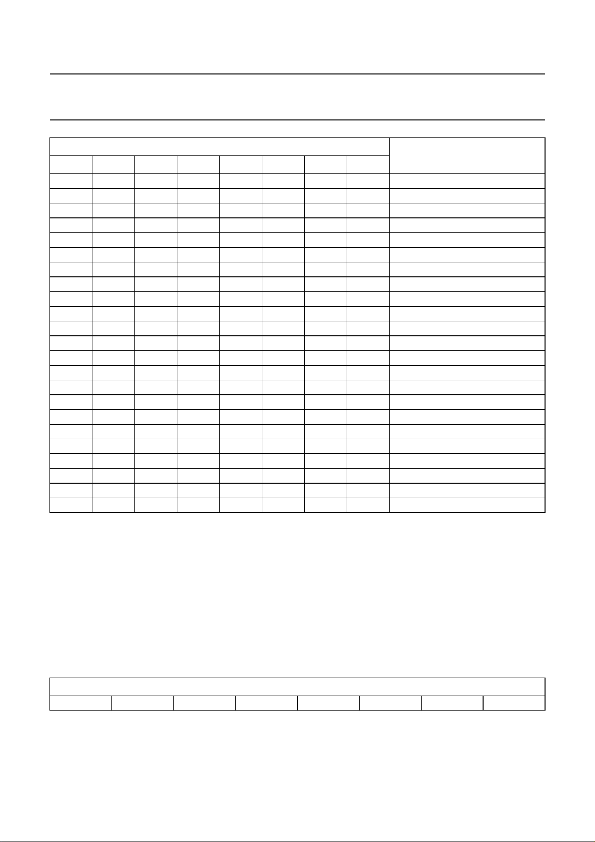
Philips Semiconductors Preliminary specification
Digital TV Sound Processor (DTVSP) TDA9875
MSB LSB
B7 B6 B5 B4 B3 B2 B1 B0
XXX00110 +6
XXX00101 +5
XXX00100 +4
XXX00011 +3
XXX00010 +2
XXX00001 +1
XXX00000 0
XXX11111 −1
XXX11110 −2
XXX11101 −3
XXX11100 −4
XXX11011 −5
XXX11010 −6
XXX11001 −7
XXX11000 −8
XXX10111 −9
XXX10110 −10
XXX10101 −11
XXX10100 −12
XXX10011 −13
XXX10010 −14
XXX10001 −15
XXX10000 mute
GAIN SETTING
(dB)
Notes
1. X = don’t care.
2. The default setting at power-up is 00000000.
10.3.13 NICAM
LOWER ERROR LIMIT REGISTER
10.3.13.1 Description
When the auto-mute function is enabled (bit AMUTE in the NICAM configuration register) and the NICAM bit error count
is lower than the value contained in this register, the NICAM signal is reselected for reproduction, see Section 10.3.14.
10.3.13.2 Definition
Table 34 Subaddress 16 (notes 1 and 2)
MSB LSB
B7 B6 B5 B4 B3 B2 B1 B0
Notes
1. The default setting at power-up is 00010100.
−5
2. The lower bit error rate limit ≅ subaddress 16 × 1.74 × 10
1998 Feb 13 44
.
Page 45
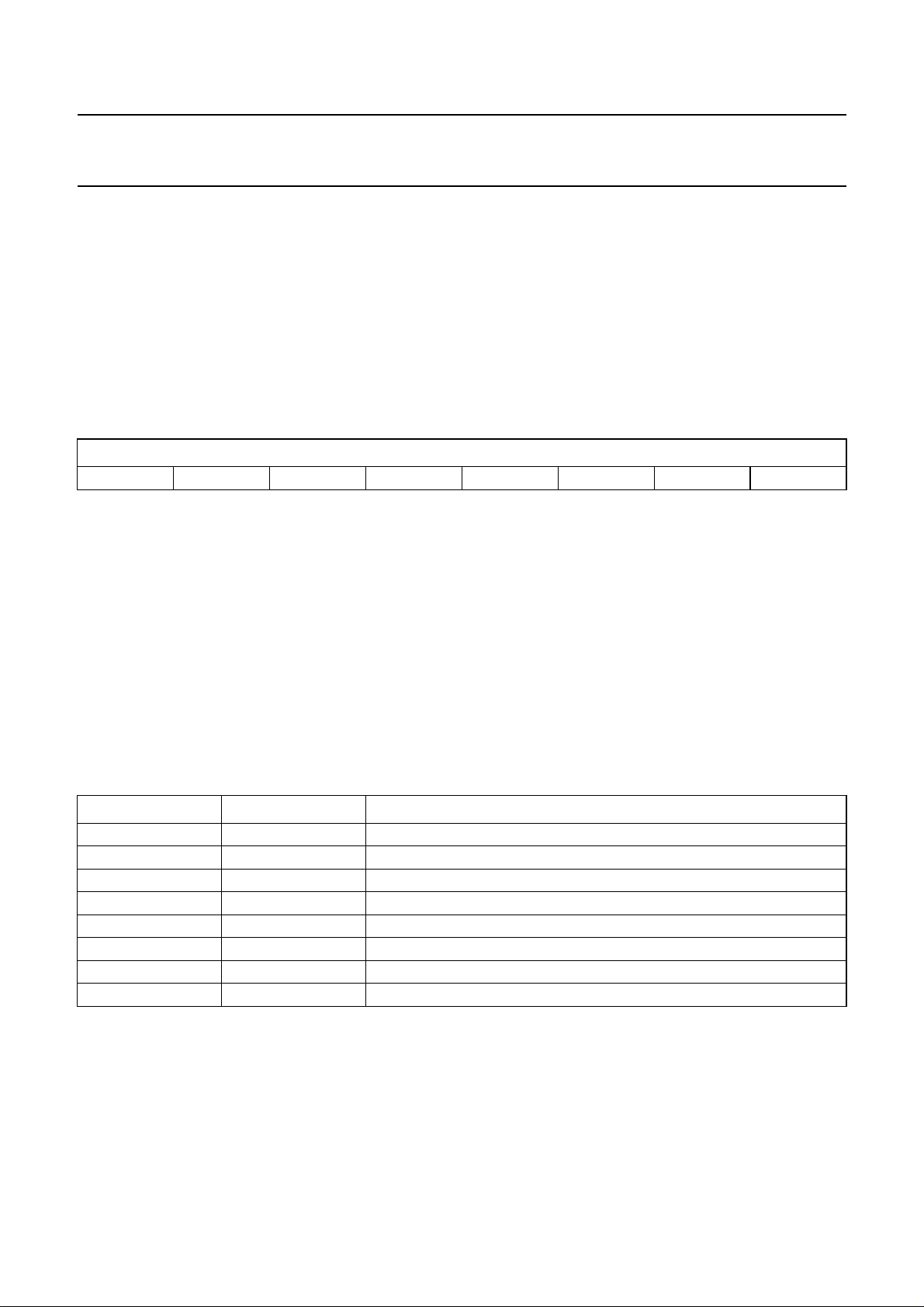
Philips Semiconductors Preliminary specification
Digital TV Sound Processor (DTVSP) TDA9875
10.3.14 NICAM UPPER ERROR LIMIT REGISTER
10.3.14.1 Description
When the auto-mute function is enabled (bit AMUTE in the NICAM configuration register) and the NICAM bit error count
is higher than the value contained in this register, the signal of the first sound carrier (i.e. FM mono or AM sound) is
selected for reproduction.
The difference between upper and lower error limit constitutes a hysteresis to avoid frequent switching between NICAM
and the program on the first sound carrier.
10.3.14.2 Definition
Table 35 Subaddress 17 (notes 1 and 2)
MSB LSB
B7 B6 B5 B4 B3 B2 B1 B0
Notes
1. The default setting at power-up is 01010000.
−5
2. The lower bit error rate limit ≅ subaddress 16 × 1.74 × 10
.
10.3.15 A
UDIO MUTE CONTROL REGISTER
10.3.15.1 Description
When any of these bits are set HIGH, the corresponding pair of output channels will be muted. A LOW bit allows normal
signal output.
There is a soft-mute facility for the Main and Auxiliary output channels to provide click-free muting independent of the
volume control. This is switched on/off by bits MUTMAIN and MUTAUX.
10.3.15.2 Definition
Table 36 Subaddress 18 (note 1)
BIT NAME DESCRIPTION
2
7 (MSB) MUTI
6 MUTI
S2 mute I2S2 outputs
2
S1 mute I2S1 outputs
5 MUTDAC mute internal DAC
4 MUTLINE mute line outputs
3 MUTSC2 mute SCART 2 outputs
2 MUTSC1 mute SCART 1 outputs
1 MUTAUX mute Auxiliary outputs
0 (LSB) MUTMAIN mute Main channels
Note
1. The default setting at power-up is 11111111.
1998 Feb 13 45
Page 46
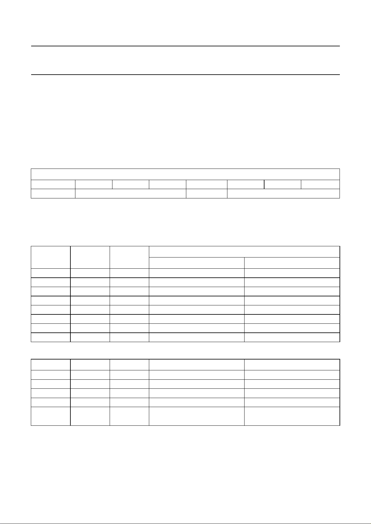
Philips Semiconductors Preliminary specification
Digital TV Sound Processor (DTVSP) TDA9875
10.3.16 DAC OUTPUT SELECT REGISTER
10.3.16.1 Description
This register is used to define both the signal source to be entered into the DAC and the mode of the digital matrix for
signal selection. The DAC is used for signal output from digital sources at analog outputs.
The two combinations of FM and NICAM apply to the (rare) condition that three different languages are being broadcast
in an FM + NICAM system. They allow for a two-out-of-three selection for external use, such as recording.
10.3.16.2 Definition
Table 37 Subaddress 19 (note 1)
MSB LSB
B7 B6 B5 B4 B3 B2 B1 B0
DACGAIN2
(2)
see Table 39 DACGAIN1
Notes
1. The default setting at power-up is 00000000.
2. See Table 40.
(2)
see Table 38
Table 38 Signal source left and right
SIGNAL SOURCE
B2 B1 B0
LEFT RIGHT
0 0 0 FM left FM right
0 0 1 NICAM left NICAM right
010 I
011 I
2
S1 left I2S1 right
2
S2 left I2S2 right
1 0 0 ADC left ADC right
1 0 1 AVL left AVL right
1 1 0 FM mono NICAM M1
1 1 1 FM mono NICAM M2
Table 39 Bits B6 to B4 (note 1)
B6 B5 B4 L OUTPUT R OUTPUT
0 0 0 L input R input
0 0 1 L input L input
0 1 0 R input R input
0 1 1 R input L input
1XX
LR+
------------- 2
LR+
------------- 2
Note
1. X = don’t care.
1998 Feb 13 46
Page 47
Philips Semiconductors Preliminary specification
Digital TV Sound Processor (DTVSP) TDA9875
Table 40 Description of bits DACGAIN1 and DACGAIN2
NAME HIGH/LOW FUNCTION
DACGAIN1, DACGAIN2 HIGH These bits can introduce some extra gain at the input to the DAC.
DACGAIN1 adds 3 dB and DACGAIN2 adds 6 dB of gain, respectively.
LOW Sets a gain of 0 dB.
10.3.17 SCART 1
OUTPUT SELECT REGISTER
10.3.17.1 Description
This register is used to define both the signal source to be output at SCART 1 and the output channel selector mode.
10.3.17.2 Definition
Table 41 Subaddress 20 (notes 1 and 2)
MSB LSB
B7 B6 B5 B4 B3 B2 B1 B0
X SC1GAIN
Notes
1. X = don’t care.
2. The default setting at power-up is 00000001.
3. See Table 44.
Table 42 Signal source
B2 B1 B0 SIGNAL SOURCE
0 0 1 SCART 2 input
0 1 0 external input
0 1 1 mono input
1 0 0 DAC input
(3)
see Table 43 X see Table 42
Table 43 Bits B5 and B4
B5 B4 L OUTPUT R OUTPUT
0 0 L input R input
0 1 L input L input
1 0 R input R input
1 1 R input L input
1998 Feb 13 47
Page 48
Philips Semiconductors Preliminary specification
Digital TV Sound Processor (DTVSP) TDA9875
Table 44 Description of bit SC1GAIN (note 1)
NAME HIGH/LOW FUNCTION
SC1GAIN HIGH Activates the 3 dB gain stage at the SCART 1 output port. As any SCART input passes
a 3 dB attenuator, this gain stage can be used to compensate that attenuation, resulting
in a 0 dB insertion loss when copying from SCART 2 input to SCART 1 output.
However, that gain must be used with great care, as it will cause signal clipping at high
input levels.
LOW The audio signal will be output unchanged (0 dB gain).
Note
1. A possibility to copy from SCART 1 input to SCART 1 output is not implemented.
10.3.18 SCART 2
OUTPUT SELECT REGISTER
10.3.18.1 Description
This register is used to define both the signal source to be output at SCART 2 and the output channel selector mode.
10.3.18.2 Definition
Table 45 Subaddress 21 (notes 1 and 2)
MSB LSB
B7 B6 B5 B4 B3 B2 B1 B0
X SC2GAIN
Notes
1. X = don’t care.
2. The default setting at power-up is 00000000.
3. See Table 48.
Table 46 Signal source
B2 B1 B0 SIGNAL SOURCE
0 0 0 SCART 1 input
0 1 0 external input
0 1 1 mono input
1 0 0 DAC input
(3)
see Table 47 X see Table 46
Table 47 Bits B5 and B4
B5 B4 L OUTPUT R OUTPUT
0 0 L input R input
0 1 L input L input
1 0 R input R input
1 1 R input L input
1998 Feb 13 48
Page 49
Philips Semiconductors Preliminary specification
Digital TV Sound Processor (DTVSP) TDA9875
Table 48 Description of bit SC2GAIN (note 1)
NAME HIGH/LOW FUNCTION
SC2GAIN HIGH Activates the 3 dB gain stage at the SCART 2 output port. As any SCART input passes
a 3 dB attenuator, this gain stage can be used to compensate that attenuation, resulting
in a 0 dB insertion loss when copying from SCART 1 input to SCART 2 output.
However, that gain must be used with great care, as it will cause signal clipping at high
input levels.
LOW The audio signal will be output unchanged (0 dB gain).
Note
1. A possibility to copy from SCART 2 input to SCART 2 output is not implemented.
10.3.19 L
INE OUTPUT SELECT REGISTER
10.3.19.1 Description
By definition, the line output conveys the same signal as the Main (loudspeaker) channel, but in a non-processed form.
This register is used to characterize the signal to be output at the line output and define the output channel selector mode.
10.3.19.2 Definition
Table 49 Subaddress 22 (note 1)
BIT NAME DESCRIPTION
7 (MSB) X don’t care
6 LINGAIN line output gain on/off; see Table 51
5 see Table 50
4
3 X don’t care
2 X don’t care
1 X don’t care
0 (LSB) LINSEL select source for line output; see Table 51
Note
1. The default setting at power-up is 00000000.
Table 50 Bits B5 and B4
B5 B4 L OUTPUT R OUTPUT
0 0 L input R input
0 1 L input L input
1 0 R input R input
1 1 R input L input
1998 Feb 13 49
Page 50
Philips Semiconductors Preliminary specification
Digital TV Sound Processor (DTVSP) TDA9875
Table 51 Description of bits LINSEL and LINGAIN
NAME HIGH/LOW FUNCTION
LINSEL HIGH Specifies that a signal from an analog source is being processed in the Main channel.
Analog signal sources comprise SCART 1 input, SCART 2 input, external input and
mono input, i.e. any input to the ADC.
LOW Specifies that a signal from a digital source is being processed in the Main channel.
Digital signal sources comprise FM, NICAM, I
LINGAIN HIGH Activates the 3 dB gain stage at the line output port.
LOW The audio signal will be output unchanged (0 dB gain).
2
S1 input and I2S2 input.
10.3.20 ADC
OUTPUT SELECT REGISTER
10.3.20.1 Description
This register is used to define the signal source for the ADC. There is no output channel selector, because all digital
signal sinks of the ADC have their own matrix. Instead, a level adjustment facility for the ADC output is provided.
10.3.20.2 Definition
Table 52 Subaddress 23 (note 1)
MSB LSB
B7 B6 B5 B4 B3 B2 B1 B0
see Table 53 see Table 54
Note
1. The default setting at power-up is 00000000.
Table 53 Signal source
B7 B6 B5 SIGNAL SOURCE
0 0 0 SCART 1 input
0 0 1 SCART 2 input
0 1 0 external input
0 1 1 mono input
Table 54 Gain setting (notes 1 and 2)
B4 B3 B2 B1 B0
01111 +15
01110 +14
01101 +13
01100 +12
01011 +11
01010 +10
01001 +9
01000 +8
00111 +7
1998 Feb 13 50
GAIN SETTING
(dB)
Page 51
Philips Semiconductors Preliminary specification
Digital TV Sound Processor (DTVSP) TDA9875
B4 B3 B2 B1 B0
00110 +6
00101 +5
00100 +4
00011 +3
00010 +2
00001 +1
00000 0
11111 −1
11110 −2
11101 −3
11100 −4
11011 −5
11010 −6
11001 −7
11000 −8
10111 −9
10110 −10
10101 −11
10100 −12
10011 −13
10010 −14
10001 −15
10000 mute
GAIN SETTING
(dB)
Notes
1. An input of the DAC output to the ADC is meaningless and, therefore, not implemented.
2. A full-scale input signal to the ADC results in an output level of −6 dB (full-scale). This occurs prior to any gain setting.
10.3.21 M
AIN CHANNEL SELECT REGISTER
10.3.21.1 Description
This register is used to define both the signal source to be processed in the Main (loudspeaker) channel and the mode
of the digital matrix for signal selection.
10.3.21.2 Definition
Table 55 Subaddress 24 (notes 1 and 2)
MSB LSB
B7 B6 B5 B4 B3 B2 B1 B0
X see Table 57 X see Table 56
Notes
1. X = don’t care.
2. The default setting at power-up is 00000000.
1998 Feb 13 51
Page 52
Philips Semiconductors Preliminary specification
Digital TV Sound Processor (DTVSP) TDA9875
Table 56 Signal source
B2 B1 B0 SIGNAL SOURCE
0 0 0 FM input
0 0 1 NICAM input
2
010 I
011 I
1 0 0 ADC input
Table 57 Bits B6 to B4 (note 1)
B6 B5 B4 L OUTPUT R OUTPUT
0 0 0 L input R input
0 0 1 L input L input
0 1 0 R input R input
0 1 1 R input L input
1XX
LR+
------------- 2
S1 input
2
S2 input
LR+
------------- 2
Note
1. X = don’t care.
10.3.22 A
UDIO EFFECTS REGISTER
10.3.22.1 Definition
Table 58 Subaddress 25 (notes 1 and 2; see Table 62)
MSB LSB
B7 B6 B5 B4 B3 B2 B1 B0
X X SPATIAL1
(3)
SPATIAL0
(3)
PSEUDO1
(4)
PSEUDO0
(4)
AVL1
(5)
Notes
1. X = don’t care.
2. The default setting at power-up is 00000000.
3. See Table 61.
4. See Table 60.
5. See Table 59.
Table 59 AVL control mode
B1 B0 AVL MODE
0 0 off/reset
0 1 short decay
1 0 medium decay
1 1 long decay
AVL0
(5)
1998 Feb 13 52
Page 53

Philips Semiconductors Preliminary specification
Digital TV Sound Processor (DTVSP) TDA9875
Table 60 Pseudo control setting
B3 B2
0 0 off
0 1 300
1 0 200
1 1 150
Table 61 Spatial control setting
B5 B4
0 0 off
0130
1040
1152
Table 62 Description of Table 58 (notes 1, 2 and 3)
NAME FUNCTION
AVL0, AVL1 These bits set the mode of operation of the automatic volume level control function at the entrance to
the Main (loudspeaker) channel.
PSEUDO0,
PSEUDO1
SPATIAL0,
SPATIAL1
These bits set the amount of the effect function (pseudo stereo) for mono signals in the Main channel.
This function should be activated only in accordance with the result of the sound mode identification.
These bits set the amount of the effect function (stereo base width expansion) for stereo signals in the
Main channel. This function should be activated only in accordance with the result of the sound mode
identification.
PSEUDO SETTING
(Hz)
SPATIAL SETTING
(%)
Notes
1. Switching the AVL off will reset the associated hardware to a defined state.
2. When the signal source for the Main channel is changed while the AVL is on, the AVL needs to be reset in order to
avoid excessive settling times. This can be achieved by switching the AVL off and on again.
3. The pseudo stereo function is based on an all-pass filter. A 90 degrees phase shift occurs at the frequencies stated
in Table 60. There is a gain of 3 dB in the audio channel containing the filter.
10.3.23 V
OLUME CONTROL REGISTERS (MAIN)
10.3.23.1 Description
These two registers control the volume setting of the Main (loudspeaker) channel. The register at subaddress 26 applies
to the left channel signal, while the register at subaddress 27 applies to the right channel signal.
Balance control is exercised by offsetting the left and right channel volume settings.
1998 Feb 13 53
Page 54
Philips Semiconductors Preliminary specification
Digital TV Sound Processor (DTVSP) TDA9875
10.3.23.2 Definition
Table 63 Subaddresses 26 and 27
MSB LSB
B7 B6 B5 B4 B3 B2 B1 B0
00011000 +24
00010111 +23
00010110 +22
00010101 +21
00010100 +20
00010011 +19
00010010 +18
00010001 +17
00010000 +16
00001111 +15
00001110 +14
00001101 +13
00001100 +12
00001011 +11
00001010 +10
00001001 +9
00001000 +8
00000111 +7
00000110 +6
00000101 +5
00000100 +4
00000011 +3
00000010 +2
00000001 +1
00000000 0
11111111 −1
11111110 −2
11111101 −3
11111100 −4
11111011 −5
11111010 −6
11111001 −7
11111000 −8
11110111 −9
11110110 −10
11110101 −11
11110100 −12
VOLUME SETTING
(dB)
1998 Feb 13 54
Page 55
Philips Semiconductors Preliminary specification
Digital TV Sound Processor (DTVSP) TDA9875
MSB LSB
B7 B6 B5 B4 B3 B2 B1 B0
11110011 −13
11110010 −14
11110001 −15
11110000 −16
11101111 −17
11101110 −18
11101101 −19
11101100 −20
11101011 −21
11101010 −22
11101001 −23
11101000 −24
11100111 −25
11100110 −26
11100101 −27
11100100 −28
11100011 −29
11100010 −30
11100001 −31
11100000 −32
11011111 −33
11011110 −34
11011101 −35
11011100 −36
11011011 −37
11011010 −38
11011001 −39
11011000 −40
11010111 −41
11010110 −42
11010101 −43
11010100 −44
11010011 −45
11010010 −46
11010001 −47
11010000 −48
11001111 −49
11001110 −50
11001101 −51
VOLUME SETTING
(dB)
1998 Feb 13 55
Page 56
Philips Semiconductors Preliminary specification
Digital TV Sound Processor (DTVSP) TDA9875
MSB LSB
B7 B6 B5 B4 B3 B2 B1 B0
11001100 −52
11001011 −53
11001010 −54
11001001 −55
11001000 −56
11000111 −57
11000110 −58
11000101 −59
11000100 −60
11000011 −61
11000010 −62
11000001 −63
11000000 −64
10111111 −65
10111110 −66
10111101 −67
10111100 −68
10111011 −69
10111010 −70
10111001 −71
10111000 −72
10110111 −73
10110110 −74
10110101 −75
10110100 −76
10110011 −77
10110010 −78
10110001 −79
10110000 −80
10101111 −81
10101110 −82
10101101 −83
10101100 mute (note 1)
VOLUME SETTING
(dB)
Note
1. The default setting at power-up is 10101100.
1998 Feb 13 56
Page 57
Philips Semiconductors Preliminary specification
Digital TV Sound Processor (DTVSP) TDA9875
10.3.24 CONTOUR CONTROL REGISTER
10.3.24.1 Description
This register is used to apply the contour or loudness function (physiological volume control) to the left and right signal
channels of the Main channel by means of an extra bass boost. The gain setting must be chosen in accordance with the
volume control setting for the Main channel. For example, the contour gain could be incremented for every 5 dB, or so,
of decrease of the volume setting. The 0 dB contour setting is equal to contour off.
10.3.24.2 Definition
Table 64 Subaddress 28 (note 1)
MSB LSB
B7 B6 B5 B4 B3 B2 B1 B0
XXX10010 18
XXX10001 17
XXX10000 16
XXX01111 15
XXX01110 14
XXX01101 13
XXX01100 12
XXX01011 11
XXX01010 10
XXX01001 9
XXX01000 8
XXX00111 7
XXX00110 6
XXX00101 5
XXX00100 4
XXX00011 3
XXX00010 2
XXX00001 1
X X X 0 0 0 0 0 0 (note 2)
CONTOUR GAIN
(dB)
Notes
1. X = don’t care.
2. The default setting at power-up is 00000000.
10.3.25 BASS CONTROL REGISTER (MAIN)
10.3.25.1 Description
This register is used to apply bass control to the left and right signal channels of the Main channel.
1998 Feb 13 57
Page 58

Philips Semiconductors Preliminary specification
Digital TV Sound Processor (DTVSP) TDA9875
10.3.25.2 Definition
Table 65 Subaddress 29 (note 1)
MSB LSB
B7 B6 B5 B4 B3 B2 B1 B0
XXX01111 +15
XXX01110 +14
XXX01101 +13
XXX01100 +12
XXX01011 +11
XXX01010 +10
XXX01001 +9
XXX01000 +8
XXX00111 +7
XXX00110 +6
XXX00101 +5
XXX00100 +4
XXX00011 +3
XXX00010 +2
XXX00001 +1
XXX00000 0 (note 2)
XXX11111 −1
XXX11110 −2
XXX11101 −3
XXX11100 −4
XXX11011 −5
XXX11010 −6
XXX11001 −7
XXX11000 −8
XXX10111 −9
XXX10110 −10
XXX10101 −11
XXX10100 −12
BASS SETTING
(dB)
Notes
1. X = don’t care.
2. The default setting at power-up is 00000000.
1998 Feb 13 58
Page 59
Philips Semiconductors Preliminary specification
Digital TV Sound Processor (DTVSP) TDA9875
10.3.26 TREBLE CONTROL REGISTER (MAIN)
10.3.26.1 Description
This register is used to apply treble control to the left and right signal channels of the Main channel.
10.3.26.2 Definition
Table 66 Subaddress 30 (note 1)
MSB LSB
B7 B6 B5 B4 B3 B2 B1 B0
XXX01100 +12
XXX01011 +11
XXX01010 +10
XXX01001 +9
XXX01000 +8
XXX00111 +7
XXX00110 +6
XXX00101 +5
XXX00100 +4
XXX00011 +3
XXX00010 +2
XXX00001 +1
X X X 0 0 0 0 0 0 (note 2)
XXX11111 −1
XXX11110 −2
XXX11101 −3
XXX11100 −4
XXX11011 −5
XXX11010 −6
XXX11001 −7
XXX11000 −8
XXX10111 −9
XXX10110 −10
XXX10101 −11
XXX10100 −12
TREBLE SETTING
(dB)
Notes
1. X = don’t care.
2. The default setting at power-up is 00000000.
1998 Feb 13 59
Page 60
Philips Semiconductors Preliminary specification
Digital TV Sound Processor (DTVSP) TDA9875
10.3.27 AUXILIARY CHANNEL SELECT REGISTER
10.3.27.1 Description
This register is used to define both the signal source to be processed in the Auxiliary (headphone) channel and the mode
of the digital matrix for signal selection.
10.3.27.2 Definition
Table 67 Subaddress 31 (notes 1 and 2)
MSB LSB
B7 B6 B5 B4 B3 B2 B1 B0
X see Table 69 X see Table 68
Notes
1. X = don’t care.
2. The default setting at power-up is 00000000.
Table 68 Signal source
B2 B1 B0 SIGNAL SOURCE
0 0 0 FM input
0 0 1 NICAM input
010 I
011 I
1 0 0 ADC input
1 0 1 AVL input
Table 69 Bits B6 to B4 (note 1)
B6 B5 B4 L OUTPUT R OUTPUT
0 0 0 L input R input
0 0 1 L input L input
0 1 0 R input R input
0 1 1 R input L input
1XX
Note
1. X = don’t care.
LR+
------------- 2
2
S1 input
2
S2 input
LR+
------------- 2
1998 Feb 13 60
Page 61
Philips Semiconductors Preliminary specification
Digital TV Sound Processor (DTVSP) TDA9875
10.3.28 VOLUME CONTROL REGISTERS (AUXILIARY)
10.3.28.1 Description
These two registers control the volume setting of the Auxiliary (headphone) channel. The register at subaddress 32
applies to the left channel signal, while the register at subaddress 33 applies to the right channel signal.
Balance control is exercised by offsetting the left and right channel volume settings.
10.3.28.2 Definition
Table 70 Subaddresses 32 and 33
MSB LSB
B7 B6 B5 B4 B3 B2 B1 B0
00011000 +24
00010111 +23
00010110 +22
00010101 +21
00010100 +20
00010011 +19
00010010 +18
00010001 +17
00010000 +16
00001111 +15
00001110 +14
00001101 +13
00001100 +12
00001011 +11
00001010 +10
00001001 +9
00001000 +8
00000111 +7
00000110 +6
00000101 +5
00000100 +4
00000011 +3
00000010 +2
00000001 +1
00000000 0
11111111 −1
11111110 −2
11111101 −3
11111100 −4
11111011 −5
11111010 −6
11111001 −7
VOLUME SETTING
(dB)
1998 Feb 13 61
Page 62
Philips Semiconductors Preliminary specification
Digital TV Sound Processor (DTVSP) TDA9875
MSB LSB
B7 B6 B5 B4 B3 B2 B1 B0
11111000 −8
11110111 −9
11110110 −10
11110101 −11
11110100 −12
11110011 −13
11110010 −14
11110001 −15
11110000 −16
11101111 −17
11101110 −18
11101101 −19
11101100 −20
11101011 −21
11101010 −22
11101001 −23
11101000 −24
11100111 −25
11100110 −26
11100101 −27
11100100 −28
11100011 −29
11100010 −30
11100001 −31
11100000 −32
11011111 −33
11011110 −34
11011101 −35
11011100 −36
11011011 −37
11011010 −38
11011001 −39
11011000 −40
11010111 −41
11010110 −42
11010101 −43
11010100 −44
11010011 −45
11010010 −46
11010001 −47
11010000 −48
VOLUME SETTING
(dB)
1998 Feb 13 62
Page 63
Philips Semiconductors Preliminary specification
Digital TV Sound Processor (DTVSP) TDA9875
MSB LSB
B7 B6 B5 B4 B3 B2 B1 B0
11001111 −49
11001110 −50
11001101 −51
11001100 −52
11001011 −53
11001010 −54
11001001 −55
11001000 −56
11000111 −57
11000110 −58
11000101 −59
11000100 −60
11000011 −61
11000010 −62
11000001 −63
11000000 −64
10111111 −65
10111110 −66
10111101 −67
10111100 −68
10111011 −69
10111010 −70
10111001 −71
10111000 −72
10110111 −73
10110110 −74
10110101 −75
10110100 −76
10110011 −77
10110010 −78
10110001 −79
10110000 −80
10101111 −81
10101110 −82
10101101 −83
10101100 mute (note 1)
VOLUME SETTING
(dB)
Note
1. The default setting at power-up is 10101100.
1998 Feb 13 63
Page 64
Philips Semiconductors Preliminary specification
Digital TV Sound Processor (DTVSP) TDA9875
10.3.29 BASS CONTROL REGISTER (AUXILIARY)
10.3.29.1 Description
This register is used to apply bass control to the left and right signal channels of the Auxiliary channel.
10.3.29.2 Definition
Table 71 Subaddress 34 (note 1)
MSB LSB
B7 B6 B5 B4 B3 B2 B1 B0
XXX01111 +15
XXX01110 +14
XXX01101 +13
XXX01100 +12
XXX01011 +11
XXX01010 +10
XXX01001 +9
XXX01000 +8
XXX00111 +7
XXX00110 +6
XXX00101 +5
XXX00100 +4
XXX00011 +3
XXX00010 +2
XXX00001 +1
XXX00000 0 (note 2)
XXX11111 −1
XXX11110 −2
XXX11101 −3
XXX11100 −4
XXX11011 −5
XXX11010 −6
XXX11001 −7
XXX11000 −8
XXX10111 −9
XXX10110 −10
XXX10101 −11
XXX10100 −12
BASS SETTING
(dB)
Notes
1. X = don’t care.
2. The default setting at power-up is 00000000.
1998 Feb 13 64
Page 65
Philips Semiconductors Preliminary specification
Digital TV Sound Processor (DTVSP) TDA9875
10.3.30 TREBLE CONTROL REGISTER (AUXILIARY)
10.3.30.1 Description
This register is used to apply treble control to the left and right signal channels of the Auxiliary channel.
10.3.30.2 Definition
Table 72 Subaddress 35 (note 1)
MSB LSB
B7 B6 B5 B4 B3 B2 B1 B0
XXX01100 +12
XXX01011 +11
XXX01010 +10
XXX01001 +9
XXX01000 +8
XXX00111 +7
XXX00110 +6
XXX00101 +5
XXX00100 +4
XXX00011 +3
XXX00010 +2
XXX00001 +1
X X X 0 0 0 0 0 0 (note 2)
XXX11111 −1
XXX11110 −2
XXX11101 −3
XXX11100 −4
XXX11011 −5
XXX11010 −6
XXX11001 −7
XXX11000 −8
XXX10111 −9
XXX10110 −10
XXX10101 −11
XXX10100 −12
TREBLE SETTING
(dB)
Notes
1. X = don’t care.
2. The default setting at power-up is 00000000.
1998 Feb 13 65
Page 66
Philips Semiconductors Preliminary specification
Digital TV Sound Processor (DTVSP) TDA9875
10.3.31 FEATURE INTERFACE CONFIGURATION REGISTER
10.3.31.1 Definition
Table 73 Subaddress 36 (notes 1 and 2)
MSB LSB
B7 B6 B5 B4 B3 B2 B1 B0
X X X SYSCL1
Notes
1. X = don’t care.
2. The default setting at power-up is 00000000.
3. System clock frequency select; see Table 74.
4. System clock output on/off; see Table 75.
5. Serial output format; see Table 75.
6. I2S-bus outputs on/off; see Table 75.
(3)
SYSCL0
(3)
SYSOUT
(4)I2
SFORM
(5)I2
SOUT
(6)
Table 74 System clock frequency select
B4 B3 SYSCLK OUTPUT FREQUENCY (MHz)
0 0 256f
0 1 384f
1 0 512f
1 1 768f
s
s
s
s
8.192
12.288
16.384
24.576
Table 75 Description of Table 73
NAME HIGH/LOW FUNCTION
2
SOUT HIGH Enables the output of serial audio data (2 pins) plus serial bit clock and word select in a
I
format determined by the I2SFORM bit. The TDA9875 is then an I2S-bus master.
LOW the outputs mentioned will be 3-stated, thereby improving the EMC performance
I2SFORM HIGH an MSB-aligned, MSB-first output format is selected, i.e. a level change at the word
select pin indicates the beginning of a new audio sample
LOW the standard I
2
S-bus output format is selected
SYSOUT HIGH enables the output of a system (or master) clock signal at pin SYSCLK
LOW the output will be off, thereby improving the EMC performance
1998 Feb 13 66
Page 67
Philips Semiconductors Preliminary specification
Digital TV Sound Processor (DTVSP) TDA9875
10.3.32 I2S1 OUTPUT SELECT REGISTER
10.3.32.1 Description
This register is used to define both the signal source to be output at I2S1 and the mode of the digital matrix for signal
selection.
10.3.32.2 Definition
Table 76 Subaddress 37 (notes 1 and 2)
MSB LSB
B7 B6 B5 B4 B3 B2 B1 B0
X see Table 78 X see Table 77
Notes
1. X = don’t care.
2. The default setting at power-up is 00000000.
Table 77 Signal source (note 1)
B2 B1 B0 SIGNAL SOURCE
0 0 0 FM output
0 0 1 NICAM output
010 I
011 I
1 0 0 ADC output
1 0 1 AVL output
1 1 0 Auxiliary output
1 1 1 Main output
Note
1. The Main and Auxiliary channel outputs will not contain the beeper signal.
Table 78 Bits B6 to B4 (note 1)
B6 B5 B4 L OUTPUT R OUTPUT
0 0 0 L input R input
0 0 1 L input L input
0 1 0 R input R input
0 1 1 R input L input
1XX
LR+
------------- 2
2
S1 input
2
S2 input
LR+
------------- 2
Note
1. X = don’t care.
1998 Feb 13 67
Page 68
Philips Semiconductors Preliminary specification
Digital TV Sound Processor (DTVSP) TDA9875
10.3.33 I2S1 INPUT LEVEL ADJUST REGISTER
10.3.33.1 Description
This register is used to adjust the input level at the I2S1 interface. Left and right signal channel are treated identically.
10.3.33.2 Definition
Table 79 Subaddress 38 (note 1)
MSB LSB
B7 B6 B5 B4 B3 B2 B1 B0
XXX01111 +15
XXX01110 +14
XXX01101 +13
XXX01100 +12
XXX01011 +11
XXX01010 +10
XXX01001 +9
XXX01000 +8
XXX00111 +7
XXX00110 +6
XXX00101 +5
XXX00100 +4
XXX00011 +3
XXX00010 +2
XXX00001 +1
XXX00000 0 (note 2)
XXX11111 −1
XXX11110 −2
XXX11101 −3
XXX11100 −4
XXX11011 −5
XXX11010 −6
XXX11001 −7
XXX11000 −8
XXX10111 −9
XXX10110 −10
XXX10101 −11
XXX10100 −12
XXX10011 −13
XXX10010 −14
XXX10001 −15
XXX10000 mute
GAIN SETTING
(dB)
Notes
1. X = don’t care.
2. The default setting at power-up is 00000000.
1998 Feb 13 68
Page 69
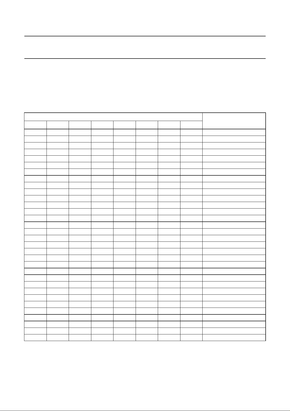
Philips Semiconductors Preliminary specification
Digital TV Sound Processor (DTVSP) TDA9875
10.3.34 I2S1 OUTPUT LEVEL ADJUST REGISTER
10.3.34.1 Description
This register is used to adjust the output level at the I2S1 interface. Left and right signal channel are treated identically.
10.3.34.2 Definition
Table 80 Subaddress 39 (note 1)
MSB LSB
B7 B6 B5 B4 B3 B2 B1 B0
XXX01111 +15
XXX01110 +14
XXX01101 +13
XXX01100 +12
XXX01011 +11
XXX01010 +10
XXX01001 +9
XXX01000 +8
XXX00111 +7
XXX00110 +6
XXX00101 +5
XXX00100 +4
XXX00011 +3
XXX00010 +2
XXX00001 +1
XXX00000 0 (note 2)
XXX11111 −1
XXX11110 −2
XXX11101 −3
XXX11100 −4
XXX11011 −5
XXX11010 −6
XXX11001 −7
XXX11000 −8
XXX10111 −9
XXX10110 −10
XXX10101 −11
XXX10100 −12
XXX10011 −13
XXX10010 −14
XXX10001 −15
XXX10000 mute
GAIN SETTING
(dB)
Notes
1. X = don’t care.
2. The default setting at power-up is 00000000.
1998 Feb 13 69
Page 70
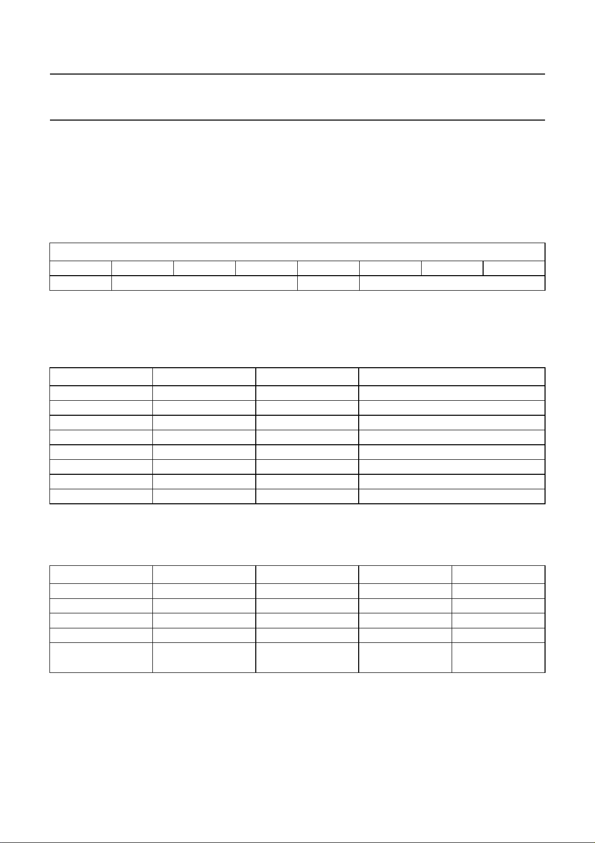
Philips Semiconductors Preliminary specification
Digital TV Sound Processor (DTVSP) TDA9875
10.3.35 I2S2 OUTPUT SELECT REGISTER
10.3.35.1 Description
This register is used to define both the signal source to be output at I2S2 and the mode of the digital matrix for signal
selection.
10.3.35.2 Definition
Table 81 Subaddress 40 (notes 1 and 2)
MSB LSB
B7 B6 B5 B4 B3 B2 B1 B0
X see Table 83 X see Table 82
Notes
1. X = don’t care.
2. The default setting at power-up is 00000000.
Table 82 Signal source (note 1)
B2 B1 B0 SIGNAL SOURCE
0 0 0 FM output
0 0 1 NICAM output
010 I
011 I
1 0 0 ADC output
1 0 1 AVL output
1 1 0 Auxiliary output
1 1 1 Main output
Note
1. The Main and Auxiliary channel outputs will not contain the beeper signal.
Table 83 Bits B6 to B4 (note 1)
B6 B5 B4 L OUTPUT R OUTPUT
0 0 0 L input R input
0 0 1 L input L input
0 1 0 R input R input
0 1 1 R input L input
1XX
LR+
------------- 2
2
S1 input
2
S2 input
LR+
------------- 2
Note
1. X = don’t care.
1998 Feb 13 70
Page 71
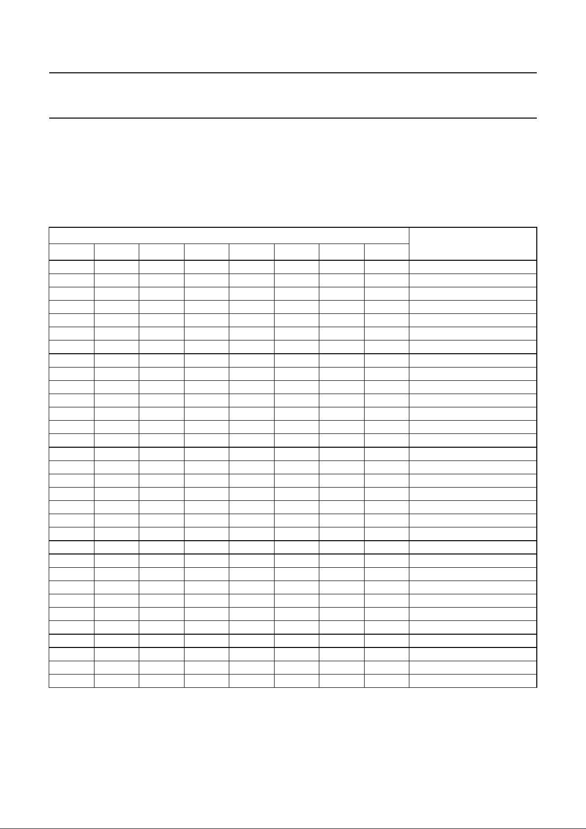
Philips Semiconductors Preliminary specification
Digital TV Sound Processor (DTVSP) TDA9875
10.3.36 I2S2 INPUT LEVEL ADJUST REGISTER
10.3.36.1 Description
This register is used to adjust the input level at the I2S2 interface. Left and right signal channel are treated identically.
10.3.36.2 Definition
Table 84 Subaddress 41 (note 1)
MSB LSB
B7 B6 B5 B4 B3 B2 B1 B0
XXX01111 +15
XXX01110 +14
XXX01101 +13
XXX01100 +12
XXX01011 +11
XXX01010 +10
XXX01001 +9
XXX01000 +8
XXX00111 +7
XXX00110 +6
XXX00101 +5
XXX00100 +4
XXX00011 +3
XXX00010 +2
XXX00001 +1
XXX00000 0 (note 2)
XXX11111 −1
XXX11110 −2
XXX11101 −3
XXX11100 −4
XXX11011 −5
XXX11010 −6
XXX11001 −7
XXX11000 −8
XXX10111 −9
XXX10110 −10
XXX10101 −11
XXX10100 −12
XXX10011 −13
XXX10010 −14
XXX10001 −15
XXX10000 mute
GAIN SETTING
(dB)
Notes
1. X = don’t care.
2. The default setting at power-up is 00000000.
1998 Feb 13 71
Page 72
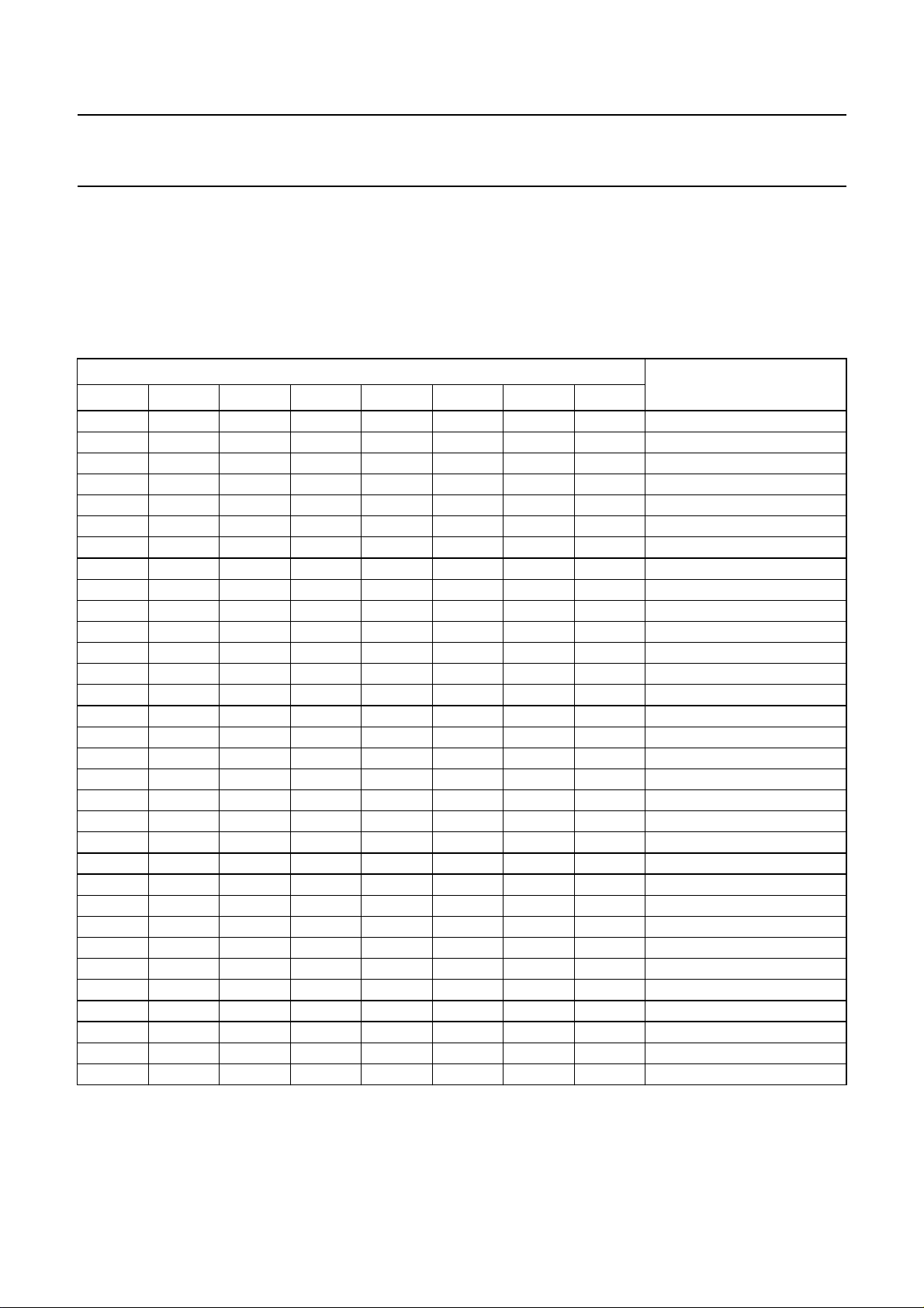
Philips Semiconductors Preliminary specification
Digital TV Sound Processor (DTVSP) TDA9875
10.3.37 I2S2 OUTPUT LEVEL ADJUST REGISTER
10.3.37.1 Description
This register is used to adjust the output level at the I2S2 interface. Left and right signal channel are treated identically.
10.3.37.2 Definition
Table 85 Subaddress 42 (note 1)
MSB LSB
B7 B6 B5 B4 B3 B2 B1 B0
XXX01111 +15
XXX01110 +14
XXX01101 +13
XXX01100 +12
XXX01011 +11
XXX01010 +10
XXX01001 +9
XXX01000 +8
XXX00111 +7
XXX00110 +6
XXX00101 +5
XXX00100 +4
XXX00011 +3
XXX00010 +2
XXX00001 +1
XXX00000 0 (note 2)
XXX11111 −1
XXX11110 −2
XXX11101 −3
XXX11100 −4
XXX11011 −5
XXX11010 −6
XXX11001 −7
XXX11000 −8
XXX10111 −9
XXX10110 −10
XXX10101 −11
XXX10100 −12
XXX10011 −13
XXX10010 −14
XXX10001 −15
XXX10000 mute
GAIN SETTING
(dB)
Notes
1. X = don’t care.
2. The default setting at power-up is 00000000.
1998 Feb 13 72
Page 73
Philips Semiconductors Preliminary specification
Digital TV Sound Processor (DTVSP) TDA9875
10.3.38 BEEPER FREQUENCY CONTROL REGISTER
10.3.38.1 Description
This register is used to select from sample beeper oscillator frequencies. The beeper output signal is added to the Main
and Auxiliary channel output DAC.
Due to the frequency response of the audio DACs upsampling filters, the 25 kHz beep is approximately 5 dB louder than
the 390 Hz beep.
10.3.38.2 Definition
Table 86 Subaddress 43 (notes 1 and 2)
MSB LSB
B7 B6 B5 B4 B3 B2 B1 B0
XXXXX111 25000
XXXXX110 7040
XXXXX101 3580
XXXXX100 1770
XXXXX011 1270
XXXXX010 900
XXXXX001 640
XXXXX000 390
Notes
1. X = don’t care.
2. The default setting at power-up is 00000000.
10.3.39 B
EEPER VOLUME CONTROL REGISTER
GENERATED FREQUENCY
(Hz)
10.3.39.1 Description
This register is used to set the beeper volume. The gain setting is relative to digital full-scale at the input to the Main and
Auxiliary channel output DACs. The beeper volume is independent of any other volume setting.
The beeper signal is added to the Main and Auxiliary channel output signals in the 2 × fs domain. The beeper volume
should be set with great care, when the audio signals in the Main and Auxiliary channels are close to digital full-scale, to
avoid output signal distortion due to overload.
1998 Feb 13 73
Page 74
Philips Semiconductors Preliminary specification
Digital TV Sound Processor (DTVSP) TDA9875
10.3.39.2 Definition
Table 87 Subaddress 44 (note 1)
MSB LSB
B7 B6 B5 B4 B3 B2 B1 B0
XX000000 0
XX111111 −3
XX111110 −6
XX111101 −9
XX111100 −12
XX111011 −15
XX111010 −18
XX111001 −21
XX111000 −24
XX110111 −27
XX110110 −30
XX110101 −33
XX110100 −36
XX110011 −39
XX110010 −42
XX110001 −45
XX110000 −48
XX101111 −51
XX101110 −54
XX101101 −57
XX101100 −60
XX101011 −63
XX101010 −66
XX101001 −69
XX101000 −72
XX100111 −75
XX100110 −78
XX100101 −81
XX100100 −84
XX100011 −87
XX100010 −90
XX100001 −93
X X 1 0 0 0 0 0 mute (note 2)
GAIN SETTING
(dB)
Notes
1. X = don’t care.
2. The default setting at power-up is 00100000.
1998 Feb 13 74
Page 75
Philips Semiconductors Preliminary specification
Digital TV Sound Processor (DTVSP) TDA9875
10.3.40 BASS BOOST CONTROL REGISTER
10.3.40.1 Description
This register is used to select from a few sample bass boost settings to modify the frequency characteristics of the Main
channel (shelving filter). Bits B3 to B0 apply to the left channel, bits B7 to B4 apply to the right channel. This function
must be used with care in order to avoid clipping distortion at high volume settings.
More sophisticated control of the bass boost filter can be exercised in the expert mode (see Section 10.5). The user then
has full control over this 2nd-order filter and can, within limits, realize bass equalizers with arbitrary centre frequencies,
Q factors and boost/cut settings.
10.3.40.2 Definition
Table 88 Subaddress 45 (note 1; see Table 89)
MSB LSB
B7 B6 B5 B4 B3 B2 B1 B0
Note
1. The default setting at power-up is 00000000.
Table 89 Gain setting
B7, B3 B6, B2 B5, B1 B4, B0
1010 20 350
1001 18 350
1000 16 350
0111 14 350
0110 12 350
0101 10 350
0100 8 350
0011 6 350
0010 4 350
0001 2 350
0000 0 350
GAIN SETTING
(dB)
CORNER FREQUENCY
(Hz)
1998 Feb 13 75
Page 76
Philips Semiconductors Preliminary specification
Digital TV Sound Processor (DTVSP) TDA9875
10.4 Slave transmitter mode
As a slave transmitter, the TDA9875 provides 13 registers with status information and data, a part of which is for Philips
internal purposes only. These registers can be accessed by means of subaddresses.
Table 90 General format for reading data from the TDA9875
S SLAVE ADDRESS 0 ACK SUBADDRESS ACK Sr SLAVE ADDRESS 1 ACK DATA NAm P
Table 91 Explanation of Tables 90 and 92
BIT FUNCTION
S START condition
SLAVE ADDRESS
0 data direction bit (write to device)
ACK
SUBADDRESS
Sr repeated START condition
1 data direction bit (read from device)
DATA data byte read from register
NAm
Am
P STOP condition
7-bit device address
acknowledge (by the slave)
address of register to read from
not acknowledge (by the master)
acknowledge (by the master)
Reading of data can start at any valid subaddress. It is allowed to read more than 1 data byte per transmission from the
TDA9875. In this situation, the subaddress is automatically incremented after each data byte, which results in reading
the sequence of data bytes from successive register locations, starting at SUBADDRESS.
Table 92 Format of a transmission using automatic incrementing of subaddresses
S SLAVE
ADDRESS
Note
1. n data bytes with auto-increment of subaddresses.
Each data byte in a read sequence, except for the last one, is acknowledged with Am (acknowledge by the master).
The subaddresses ‘wrap around’ from decimal 255 to 0. If an attempt is made to read from a non-existing subaddress,
the device will send a data pattern of all ones, i.e. FF in hexadecimal notation.
0 ACK SUBADDRESS ACK Sr SLAVE
ADDRESS
1 ACK DATA BYTE
Am
(1)
DATA NAm P
1998 Feb 13 76
Page 77
Philips Semiconductors Preliminary specification
Digital TV Sound Processor (DTVSP) TDA9875
Table 93 Overview of the slave transmitter registers (note 1)
SUBADDRESS
(DECIMAL)
0 ssssssssdevice status (power-on, identification, etc.)
1 ssssssssNICAM status
2 eeeeeeeeNICAM error count
3 ddddddddadditional data (LSB)
4 c c X c c d d d additional data (MSB)
5 lllllllllevel read-out (MSB)
6 lllllllllevel read-out (LSB)
7 XXXcccccSIF level
251 aaaaaaaatest register 3
252 aaaaaaaatest register 2
253 aaaaaaaatest register 1
254 dddddddddevice identification code
255 sssssssssoftware identification code
Note
1. X indicates a bit that has not yet been assigned to a function. Its meaning is ‘don’t care’, its return value is a zero.
Registers from subaddress 251 to 255 are for Philips internal purposes only. They are considered as a set of registers
for the identification of individual members and some key parameters in a family of devices.
MSB LSB
DATA
FUNCTION
A detailed description of the slave transmitter registers is given in below:
10.4.1 D
EVICE STATUS REGISTER
10.4.1.1 Definition
Table 94 Subaddress 0
BIT NAME DESCRIPTION
7 (MSB) P2IN input from port 2
6 P1IN input from port 1
5 RSSF reserve sound switching flag
4 AMSTAT auto-mute status
3 VDSP identification of NICAM sound
2 IDDUA identification of FM dual sound
1 IDSTE identification of FM stereo
0 (LSB) X don’t care
1998 Feb 13 77
Page 78
Philips Semiconductors Preliminary specification
Digital TV Sound Processor (DTVSP) TDA9875
10.4.1.2 Description
Table 95 Description of Table 94
NAME HIGH/LOW FUNCTION
IDSTE HIGH this bit is HIGH if an FM stereo signal has been identified
LOW
IDDUA − This bit is HIGH if an FM dual-language signal has been identified. When neither
IDSTE nor IDDUA are set, the received signal is assumed to be FM mono.
VDSP HIGH indicates that digital transmission is a sound source (NICAM)
LOW the transmission is either data or currently undefined format (NICAM)
AMSTAT − if this bit is HIGH, it indicates that the auto-muting function has switched from
NICAM to the program of the first sound carrier (i.e. FM mono or AM in NICAM L
systems)
RSSF HIGH This bit is a copy of the C4 bit in the NICAM status register . It indicates that the FM
(or AM for standard L) sound matches the digital transmission and auto-muting
should be enabled.
LOW auto-muting should be disabled, as analog and digital sound are different
P1IN, P2IN − these bits reflect the status of the corresponding general purpose port pins,
see Section 10.3.2
10.4.2 NICAM STATUS REGISTER
10.4.2.1 Definition
Table 96 Subaddress 1
BIT NAME DESCRIPTION
7 (MSB) C4 NICAM application control bits
6C3
5C2
4C1
3 OSB synchronization bit
2 CFC configuration change
1 S/MB identification of NICAM stereo
0 (LSB) D/SB identification of NICAM dual mono
1998 Feb 13 78
Page 79
Philips Semiconductors Preliminary specification
Digital TV Sound Processor (DTVSP) TDA9875
10.4.2.2 Description
Table 97 Description of Table 96
NAME HIGH/LOW FUNCTION
D/SB HIGH if this bit is HIGH it indicates dual mono mode
LOW
S/MB HIGH if this bit is HIGH it indicates stereo mode
LOW
CFC HIGH if this bit is HIGH, it indicates a configuration change at the 16 frame (C0)
LOW
OSB HIGH indicates that the device has both frame and C0 (16 frame) synchronization
LOW the audio output from the NICAM part should be digital silence
C1, C2, C3, C4 HIGH these bits correspond to the control bits C1 to C4 in the NICAM transmission
LOW
10.4.2.3 Notes
boundary
The TDA9875 does not support the Extended Control Modes. Therefore, the program of the first sound carrier
(i.e. FM mono or AM) is selected for reproduction in case bit C3 is set HIGH, independent of bit AMUTE in the NICAM
configuration register being set or not.
When a NICAM transmitter is switched off, the device will lose synchronization. In this situation the program of the first
sound carrier is selected for reproduction, independent of bit AMUTE being set or not.
10.4.3 NICAM
ERROR COUNT REGISTER
10.4.3.1 Description
Bits B7 to B0 contain the number of errors occurring in the previous 128 ms period. The register is updated every 128 ms.
10.4.3.2 Definition
Table 98 Subaddress 2
MSB LSB
B7 B6 B5 B4 B3 B2 B1 B0
1998 Feb 13 79
Page 80
Philips Semiconductors Preliminary specification
Digital TV Sound Processor (DTVSP) TDA9875
10.4.4 ADDITIONAL DATA REGISTERS
10.4.4.1 Description
These two bytes provide information on the additional data bits. ADBYTE0 is stored at subaddress 3.
10.4.4.2 Definition
Table 99 Subaddress 3
BIT NAME
7 (MSB) AD7
6 AD6
5 AD5
4 AD4
3 AD3
2 AD2
1 AD1
0 (LSB) AD0
Table 100 Subaddress 4
BIT NAME
7 (MSB) OVW
6 SAD
5 X (don’t care)
4 CI1
3 CI2
2 AD10
1 AD9
0 (LSB) AD8
Table 101 Description of Tables 99 and 100
NAME HIGH/LOW FUNCTION
AD10 to AD0 − comprise the additional data word
CI1, CI2 − these are CI bits decoded by majority logic from the parity checks of the last ten
samples in a frame
SAD HIGH new additional data is written into the IC
LOW reset, when the additional data bits are read
OVW − if this bit is HIGH, new additional data bits are written to the IC without the previous
bits being read
1998 Feb 13 80
Page 81

Philips Semiconductors Preliminary specification
Digital TV Sound Processor (DTVSP) TDA9875
10.4.5 LEVEL READ-OUT REGISTERS
10.4.5.1 Description
These two bytes constitute a word that provides data from
a location that has been specified with the monitor select
register. The most significant byte of the data is stored at
subaddress 5.
If peak-level monitoring has been selected, the peak-level
monitoring register is cleared and monitoring resumes
after its contents has been transferred to these two bytes.
10.4.5.2 Definition
Table 102 Subaddress 5
BIT
7 (most significant bit or sign bit)
6
5
4
3
2
1
0
Table 103 Subaddress 6
BIT
7
6
5
4
3
2
1
0 (least significant bit)
10.4.6 SIF LEVEL REGISTER
10.4.6.1 Description
When the SIF AGC is on, bits B4 to B0 of this register
contain a number that gives an indication of the SIF input
level. That number can be interpreted in the same way as
the AGC gain register setting (see Section 10.3,
subaddress 0), i.e., if the SIF AGC were set to a fixed gain
and the same number loaded into the AGC gain register,
the current SIF input signal level would generate an SIF
ADC output close to full-scale.
When the SIF AGC is off, this register returns the contents
of the AGC gain register.
10.4.6.2 Definition
Table 104 Subaddress 7 (note 1)
MSB LSB
B7 B6 B5 B4 B3 B2 B1 B0
Note
1. Bits B5, B6 and B7 are don’t care.
10.4.7 T
EST REGISTER 3
10.4.7.1 Description
This register contains, as a binary number, the highest
memory address used for the Coefficient RAM (CRAM,
expert mode).
The first version will have the identification 01111111.
10.4.7.2 Definition
Table 105 Subaddress 251
MSB LSB
B7 B6 B5 B4 B3 B2 B1 B0
10.4.8 TEST REGISTER 2
10.4.8.1 Description
This register contains, as a binary number, the highest
subaddress used for slave receiver registers.
The first version will have the identification 00101101.
10.4.8.2 Definition
Table 106 Subaddress 252
MSB LSB
B7 B6 B5 B4 B3 B2 B1 B0
10.4.9 TEST REGISTER 1
10.4.9.1 Description
This register contains, as a binary number, the highest
subaddress used for slave transmitter (status) registers.
The first version will have the identification 00000111.
1998 Feb 13 81
Page 82

Philips Semiconductors Preliminary specification
Digital TV Sound Processor (DTVSP) TDA9875
10.4.9.2 Definition
Table 107 Subaddress 253
MSB LSB
B7 B6 B5 B4 B3 B2 B1 B0
10.4.10 DEVICE IDENTIFICATION CODE
10.4.10.1 Description
There will be several devices in the digital TV sound
processor family, with TDA9875 being the first member.
This byte is used to identify the individual family members
purely for Philips internal use.
The first version will have the identification 00000000.
10.4.10.2 Definition
Table 108 Subaddress 254
MSB LSB
B7 B6 B5 B4 B3 B2 B1 B0
10.4.11 SOFTWARE IDENTIFICATION CODE
10.4.11.1 Description
10.4.11.2 Definition
Table 109 Subaddress 255
MSB LSB
B7 B6 B5 B4 B3 B2 B1 B0
10.5 Expert mode
In addition to the slave receiver and slave transmitter
modes previously described, there is a special ‘expert’
mode that gives direct write access to the internal CRAM
of the DSP.
In this mode, transferred data contain 12-bit-wide
coefficients. As those coefficients bypass on-chip
coefficient look-up tables for many functions, they directly
influence the processing of signals within the DSP.
This mode must be used with great care. It can be used to
create user-defined characteristics, such as a tone control
with different corner frequencies or special boost/cut
characteristics to correct the low-frequency loudspeaker
and/or cabinet frequency responses.
It is likely that during the life time of this family of devices
several versions of the DSP software will be made, e.g., to
accommodate new application concepts, respond to
customer wishes, etc. This byte is used to identify the
different releases purely for Philips internal use.
The first version will have the identification 00000000.
Table 110 General format for entering the expert mode and writing coefficients into the TDA9875
S SLAVE ADDRESS 0 ACK 10000000 ACK CRAM ADDRESS ACK DATA ACK DATA ACK P
Table 111 Explanation of Table 110
BIT FUNCTION
S START condition
SLAVE ADDRESS
0 data direction bit (write to device)
ACK
10000000
CRAM ADDRESS start address of coefficient RAM to write to
DATA data byte containing part of a coefficient
P STOP condition
7-bit device address
acknowledge
pattern to enter the expert mode
1998 Feb 13 82
Page 83
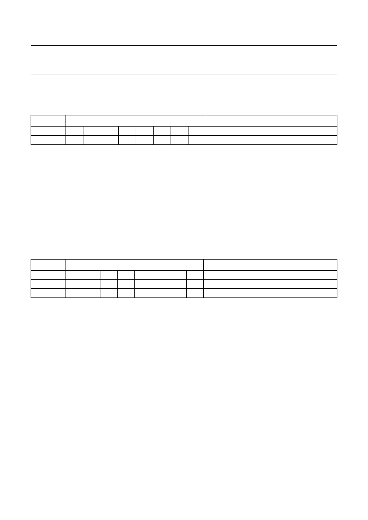
Philips Semiconductors Preliminary specification
Digital TV Sound Processor (DTVSP) TDA9875
As the coefficients do not fit into one data byte, they have to be split and arranged (see Table 112). The most significant
bit is transferred first.
Table 112 General format (notes 1, 2 and 3)
BYTE DATA DESCRIPTION
1. data byte aaaaaaaa2MST of 1st coefficient
2. data byte aaaaXXXX1LST of 1st coefficient
Notes
1. X = don’t care.
2. MST = most significant third.
3. LST = least significant third.
The general format described in Table 112 shows the minimum number of data bytes required, i.e. two bytes for the
transfer of a single coefficient.
Should more than one coefficient be sent, then the CRAM address will be automatically incremented after each
coefficient, resulting in writing the sequence of coefficients into successive memory locations, starting at
CRAM ADDRESS. A transmission can start with any valid CRAM address. If two coefficients are to be transferred, they
are arranged as shown in Table 113.
Table 113 Transfer of two coefficients
BYTE DATA DESCRIPTION
1 data byte a a a a a a a a 2 MST of 1st coefficient
2 data byte a a a a b b b b 1 LST of 1st coefficient + 1 MST of 2nd coefficient
3 data byte b b b b b b b b 2 LST of 2nd coefficient
With any odd number of coefficients to be transferred, the
least significant nibble of the last byte is regarded as
containing don’t care data.
As the transfer of coefficients cannot be accomplished
within one audio sample period, it is necessary that
received coefficients be buffered and made active all at
the same time to avoid audio signal transients. The
receive buffer is designed to store up to 8 coefficients in
addition to the CRAM address. Each byte that fits into the
buffer is acknowledged with ACK (acknowledge). If an
attempt is made to write more coefficients than the buffer
can store, the device acknowledges with NACK (not
acknowledge) and any further coefficients are ignored.
Coefficients that are already in the receive buffer remain
intact.
An expert mode transfers ends when the I2C-bus STOP
condition or a repeated START condition has been
detected. Only those coefficients that have been received
during the last transmission will then be copied from the
buffer to the CRAM.
To make efficient and correct use of the expert mode, it is
recommended to transfer all coefficients for any one
function in a single transmission.
There is no checking of memory addresses and the
automatic incrementing of addresses does not stop at the
highest used CRAM address. The user of this expert
mode must be fully acquainted with the relevant
procedures.
More information concerning the functions of this device,
such as filter structures, the number of coefficients per
function, their default values, memory addresses, etc.,
can be supplied on request at a later date.
2
S-BUS DESCRIPTION
11 I
The feature interface of the TDA9875 contains two serial
audio inputs and outputs and associated clock signals.
It can be used to supply, for example, audio signals from
received TV programs to a digital audio output device
(AES/EBU format), or import serial audio signals from
other sources for reproduction through the TV set’s
1998 Feb 13 83
Page 84

Philips Semiconductors Preliminary specification
Digital TV Sound Processor (DTVSP) TDA9875
loudspeaker and/or headphone channels. Apart from such
simple data input or output, it is also possible to run audio
signals through an external DSP, which performs some
additional functions, such as room simulation, Dolby
Surround Pro Logic etc. and feed those signals back into
the loudspeaker and/or headphone channels of the
TDA9875.
Two serial audio formats are supported at the feature
interface, i.e. the I2S-bus format and a very similar
MSB-aligned format. The difference is illustrated in Fig.7.
In both formats the left audio channel of a stereo sample
pair is output first and is placed on the serial data line (SDI
for input, SDO for output) when the word select line (WS)
is LOW. Data is written at the trailing edge of SCK and
read at the leading edge of SCK. The most significant bit
is sent first.
At power-up, the outputs of the feature interface are
3-stated to reduce EMC and allow for combinations with
other ICs. If output is desired, it has to be activated by
means of an I2C-bus command.
When the output is enabled, the serial audio data can be
taken from pins SDO1 and SDO2. Depending on the signal
source, switch and matrix positions, the output can be
either mono, stereo or dual language sound on either
output.
The word select output is clocked with the audio sample
frequency at 32 kHz. The serial clock output (SCK) is
clocked at a frequency of 2.048 MHz. This means, that
there are 64 clock pulses per pair of stereo output
samples, or 32 clock pulses per sample. Depending again
on the signal source, the number of significant bits on the
serial data outputs, SDO1 and SDO2, is between
14 and 18.
Apart from just feeding a digital audio device, such as a
DAC or an AES/EBU transmitter, the serial data outputs
can be connected directly to the serial inputs (loop-back
connection) or first to an external device, e.g. a feature
DSP such as the SAA7710 and then back to the serial
inputs. In all of these configurations, the SCK and WS
clocks will be generated by the TDA9875, which then is the
I2S-bus master.
The serial data inputs, SDI1 and SDI2, are active at all
times, independent of the serial data outputs being on or
off.
When the serial data outputs are off (either after power-up
or via the appropriate I2C-bus command) serial data and
clocks WS and SCK from a separate digital audio source
can be fed into the TDA9875, be processed and output in
accordance with internal selector positions, provided that
the following criteria are met:
• 32 kHz audio sample frequency
• 32 clock bits per sample
• External timing and data synchronized to TDA9875.
In such cases, the external source is the I2S-bus master
and the TDA9875 is the I2S-bus slave.
To support synchronization of external devices or as a
master clock for them, a symmetrical system clock output,
SYSCLK, is available from the TDA9875. At power-up it is
off. It can be enabled and the output frequency set via an
I2C-bus command. Available output frequencies are
8.192, 12.288, 16.384 and 24.576 MHz.
1998 Feb 13 84
Page 85
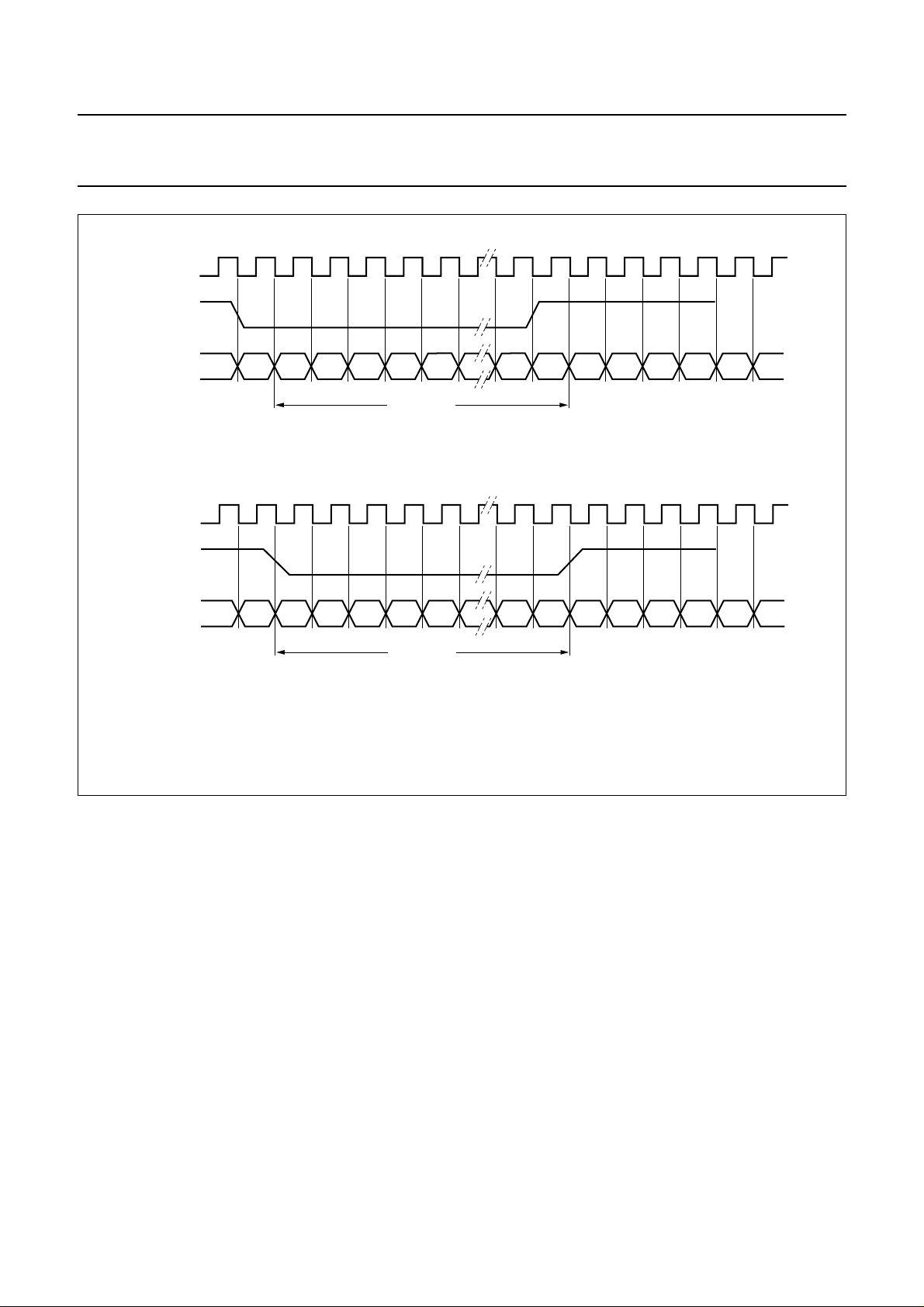
Philips Semiconductors Preliminary specification
Digital TV Sound Processor (DTVSP) TDA9875
handbook, full pagewidth
SCK
WS
SD LSB MSB
handbook, full pagewidth
SCK
WS
SD LSB MSB
LSB MSB
MGK112
one sample
a. I2S-bus format.
LSB MSB
MGK113
one sample
b. MSB-aligned format.
Fig.7 Serial audio interface formats.
1998 Feb 13 85
Page 86
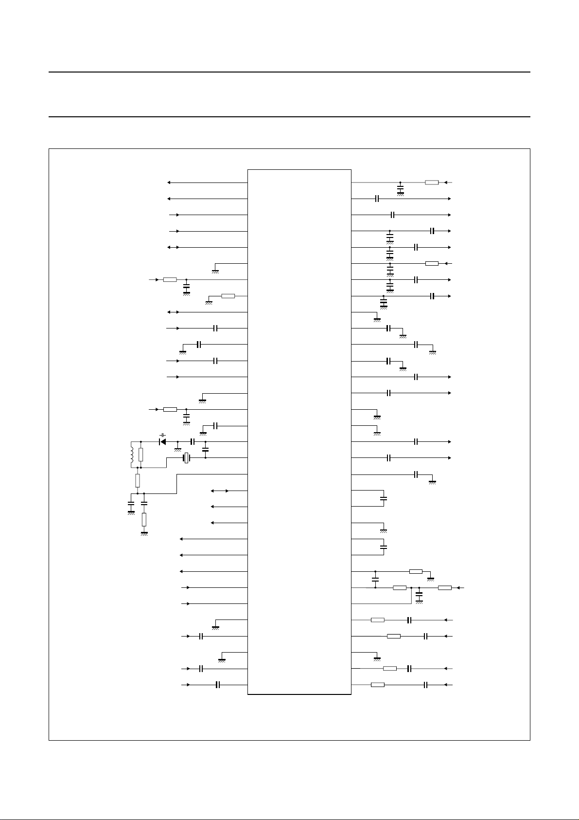
Philips Semiconductors Preliminary specification
Digital TV Sound Processor (DTVSP) TDA9875
12 EXTERNAL COMPONENTS
handbook, full pagewidth
3.3 µH
C10
33 nF
+5 V
+5 V
L1
PCLK
NICAM data
ADDR1
SCL
SDA
SIFSAT
SIFTV
ADDR2
BB135
R4
39 kΩ
R5
10 kΩ
C9
330 nF
R15
20 kΩ
MONOIN
R1
10 Ω
P1
R3
1.5 Ω
D1
SDO2
SDO1
SDI2
SDI1
EXTR
EXTL
C7
33 pF
24.576 MHz
SYSCLK
WS
C1
4.7 µF
C3
100 nF
C5
47 µF
SCK
C11
470 nF
C12
470 nF
P2
C2
47 pF
C4
47 pF
C6
1 µF
C8
33 pF
C13
470 nF
PCLK
NICAM
ADDR1
SDA
V
SSA1
V
DDA1
R2
10 kΩ
SIF2
V
SIF1
ADDR2
V
SSD1
V
DDD1
CRESET
XTALO
XTALI
V
tune
SYSCLK
SCK
SDO2
SDO1
SDI2
SDI1
TEST1
MONOIN
TEST2
EXTIR
EXTIL
SCL
I
ref1
WS
47 µF
2.2 µF
2.2 µF
C27
10 nF
C29
2.2 µF
2.2 µF
47 µF
270 Ω
C38
330 nF
C40
330 nF
C19
C22
C31
C33
R8
1.5 Ω
2.2 µF
10 Ω
2.2 µF
C37
47 µF
C39
330 nF
C41
330 nF
R7
C17
R6
C24
R10
10 Ω
+5 V
LINER
LINEL
MAINL
MAINR
+5 V
AUXL
AUXR
SC2OL
SC2OR
SC1OL
SC1OR
+5 V
SC2IL
SC2IR
SC1IL
SC1IR
V
MGK114
64
63
62
61
60
59
58
57
56
55
54
53
52
51
50
49
48
47
46
45
44
43
42
41
40
39
38
37
36
35
34
33
DDD2
LOR
LOL
MOL
MOR
V
DDA3
AUXOL
AUXOR
V
SSA3
PCAPL
PCAPR
V
ref3
SCOL2
SCOR2
V
SSA4
V
SSD2
SCOL1
SCOR1
V
ref2
CAPR1
CAPR2
V
SSA2
CAPL2
CAPL1
V
ref(n)
V
ref(p)
V
DDA2
SCIL2
SCIR2
V
SSG
SCIL1
SCIR1
C14
C15
2.2 µF
C16
2.2 µF
C18
C20 10 nF
C21
C23 10 nF
10 nF
C25
C26
10 nF
C28
47 µF
C30
2.2 µF
C32
2.2 µF
C34
220 pF
C35
220 pF
C36
47 µF
R11
15 kΩ
R12
15 kΩ
R13
15 kΩ
R14
15 kΩ
10 nF
47 µF
R9
270 Ω
1
2
3
4
5
6
7
ref
8
P1
9
10
11
12
13
14
15
16
17
18
19
P2
20
21
22
23
24
25
26
27
28
29
30
31
32
TDA9875
Fig.8 Schematic for measurements.
1998 Feb 13 86
Page 87
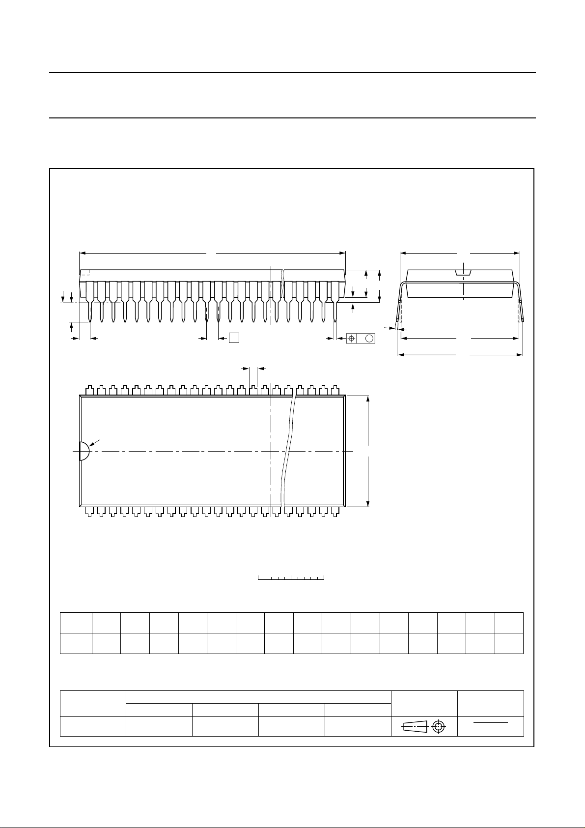
Philips Semiconductors Preliminary specification
Digital TV Sound Processor (DTVSP) TDA9875
13 PACKAGE OUTLINE
SDIP64: plastic shrink dual in-line package; 64 leads (750 mil)
D
seating plane
L
Z
64
pin 1 index
e
b
SOT274-1
M
E
A
2
A
A
1
w M
b
1
33
E
c
(e )
M
1
H
1
0 5 10 mm
scale
DIMENSIONS (mm are the original dimensions)
A
A
A
UNIT b
Note
1. Plastic or metal protrusions of 0.25 mm maximum per side are not included.
mm
OUTLINE
VERSION
SOT274-1
max.
5.84
12
min.
max.
4.57
0.51
IEC JEDEC EIAJ
1.3
0.8
b
1
0.53
0.40
REFERENCES
0.32
0.23
cEe M
(1) (1)
D
58.67
57.70
1998 Feb 13 87
17.2
16.9
32
(1)
Z
e
1
L
M
E
3.2
19.61
2.8
19.05
EUROPEAN
PROJECTION
20.96
19.71
w
H
0.181.778 19.05
ISSUE DATE
92-10-13
95-02-04
max.
1.73
Page 88

Philips Semiconductors Preliminary specification
Digital TV Sound Processor (DTVSP) TDA9875
14 SOLDERING
14.1 Introduction
There is no soldering method that is ideal for all IC
packages. Wave soldering is often preferred when
through-hole and surface mounted components are mixed
on one printed-circuit board. However, wave soldering is
not always suitable for surface mounted ICs, or for
printed-circuits with high population densities. In these
situations reflow soldering is often used.
This text gives a very brief insight to a complex technology.
A more in-depth account of soldering ICs can be found in
our
“IC Package Databook”
(order code 9398 652 90011).
14.2 Soldering by dipping or by wave
The maximum permissible temperature of the solder is
260 °C; solder at this temperature must not be in contact
with the joint for more than 5 seconds. The total contact
time of successive solder waves must not exceed
5 seconds.
The device may be mounted up to the seating plane, but
the temperature of the plastic body must not exceed the
specified maximum storage temperature (T
stg max
). If the
printed-circuit board has been pre-heated, forced cooling
may be necessary immediately after soldering to keep the
temperature within the permissible limit.
14.3 Repairing soldered joints
Apply a low voltage soldering iron (less than 24 V) to the
lead(s) of the package, below the seating plane or not
more than 2 mm above it. If the temperature of the
soldering iron bit is less than 300 °C it may remain in
contact for up to 10 seconds. If the bit temperature is
between 300 and 400 °C, contact may be up to 5 seconds.
15 DEFINITIONS
Data sheet status
Objective specification This data sheet contains target or goal specifications for product development.
Preliminary specification This data sheet contains preliminary data; supplementary data may be published later.
Product specification This data sheet contains final product specifications.
Limiting values
Limiting values given are in accordance with the Absolute Maximum Rating System (IEC 134). Stress above one or
more of the limiting values may cause permanent damage to the device. These are stress ratings only and operation
of the device at these or at any other conditions above those given in the Characteristics sections of the specification
is not implied. Exposure to limiting values for extended periods may affect device reliability.
Application information
Where application information is given, it is advisory and does not form part of the specification.
16 LIFE SUPPORT APPLICATIONS
These products are not designed for use in life support appliances, devices, or systems where malfunction of these
products can reasonably be expected to result in personal injury. Philips customers using or selling these products for
use in such applications do so at their own risk and agree to fully indemnify Philips for any damages resulting from such
improper use or sale.
17 PURCHASE OF PHILIPS I
Purchase of Philips I
2
C COMPONENTS
2
C components conveys a license under the Philips’ I2C patent to use the
components in the I2C system provided the system conforms to the I2C specification defined by
Philips. This specification can be ordered using the code 9398 393 40011.
1998 Feb 13 88
Page 89

Philips Semiconductors Preliminary specification
Digital TV Sound Processor (DTVSP) TDA9875
NOTES
1998 Feb 13 89
Page 90

Philips Semiconductors Preliminary specification
Digital TV Sound Processor (DTVSP) TDA9875
NOTES
1998 Feb 13 90
Page 91

Philips Semiconductors Preliminary specification
Digital TV Sound Processor (DTVSP) TDA9875
NOTES
1998 Feb 13 91
Page 92

Philips Semiconductors – a worldwide company
Argentina: see South America
Australia: 34 Waterloo Road, NORTH RYDE, NSW 2113,
Tel. +61 2 9805 4455, Fax. +61 2 9805 4466
Austria: Computerstr. 6, A-1101 WIEN, P.O. Box 213, Tel. +43 160 1010,
Fax. +43 160 101 1210
Belarus: Hotel Minsk Business Center, Bld. 3, r. 1211, Volodarski Str. 6,
220050 MINSK, Tel. +375 172 200 733, Fax. +375 172 200 773
Belgium: see The Netherlands
Brazil: see South America
Bulgaria: Philips Bulgaria Ltd., Energoproject, 15th floor,
51 James Bourchier Blvd., 1407 SOFIA,
Tel. +359 2 689 211, Fax. +359 2 689 102
Canada: PHILIPS SEMICONDUCTORS/COMPONENTS,
Tel. +1 800 234 7381
China/Hong Kong: 501 Hong Kong Industrial Technology Centre,
72 Tat Chee Avenue, Kowloon Tong, HONG KONG,
Tel. +852 2319 7888, Fax. +852 2319 7700
Colombia: see South America
Czech Republic: see Austria
Denmark: Prags Boulevard 80, PB 1919, DK-2300 COPENHAGEN S,
Tel. +45 32 88 2636, Fax. +45 31 57 0044
Finland: Sinikalliontie 3, FIN-02630 ESPOO,
Tel. +358 9 615800, Fax. +358 9 61580920
France: 51 Rue Carnot, BP317, 92156 SURESNES Cedex,
Tel. +33 1 40 99 6161, Fax. +33 1 40 99 6427
Germany: Hammerbrookstraße 69, D-20097 HAMBURG,
Tel. +49 40 23 53 60, Fax. +49 40 23 536 300
Greece: No. 15, 25th March Street, GR 17778 TAVROS/ATHENS,
Tel. +30 1 4894 339/239, Fax. +30 1 4814 240
Hungary: see Austria
India: Philips INDIA Ltd, Band Box Building, 2nd floor,
254-D, Dr. Annie Besant Road, Worli, MUMBAI 400 025,
Tel. +91 22 493 8541, Fax. +91 22 493 0966
Indonesia: see Singapore
Ireland: Newstead, Clonskeagh, DUBLIN 14,
Tel. +353 1 7640 000, Fax. +353 1 7640 200
Israel: RAPAC Electronics, 7 Kehilat Saloniki St, PO Box 18053,
TEL AVIV 61180, Tel. +972 3 645 0444, Fax. +972 3 649 1007
Italy: PHILIPS SEMICONDUCTORS, Piazza IV Novembre 3,
20124 MILANO, Tel. +39 2 6752 2531, Fax. +39 2 6752 2557
Japan: Philips Bldg 13-37, Kohnan 2-chome, Minato-ku, TOKYO 108,
Tel. +81 3 3740 5130, Fax. +81 3 3740 5077
Korea: Philips House, 260-199 Itaewon-dong, Yongsan-ku, SEOUL,
Tel. +82 2 709 1412, Fax. +82 2 709 1415
Malaysia: No. 76 Jalan Universiti, 46200 PETALING JAYA, SELANGOR,
Tel. +60 3 750 5214, Fax. +60 3 757 4880
Mexico: 5900 Gateway East, Suite 200, EL PASO, TEXAS 79905,
Tel. +9-5 800 234 7381
Middle East: see Italy
Netherlands: Postbus 90050, 5600 PB EINDHOVEN, Bldg. VB,
Tel. +31 40 27 82785, Fax. +31 40 27 88399
New Zealand: 2 Wagener Place, C.P.O. Box 1041, AUCKLAND,
Tel. +64 9 849 4160, Fax. +64 9 849 7811
Norway: Box 1, Manglerud 0612, OSLO,
Tel. +47 22 74 8000, Fax. +47 22 74 8341
Philippines: Philips Semiconductors Philippines Inc.,
106 Valero St. Salcedo Village, P.O. Box 2108 MCC, MAKATI,
Metro MANILA, Tel. +63 2 816 6380, Fax. +63 2 817 3474
Poland: Ul. Lukiska 10, PL 04-123 WARSZAWA,
Tel. +48 22 612 2831, Fax. +48 22 612 2327
Portugal: see Spain
Romania: see Italy
Russia: Philips Russia, Ul. Usatcheva 35A, 119048 MOSCOW,
Tel. +7 095 755 6918, Fax. +7 095 755 6919
Singapore: Lorong 1, Toa Payoh, SINGAPORE 1231,
Tel. +65 350 2538, Fax. +65 251 6500
Slovakia: see Austria
Slovenia: see Italy
South Africa: S.A. PHILIPS Pty Ltd., 195-215 Main Road Martindale,
2092 JOHANNESBURG, P.O. Box 7430 Johannesburg 2000,
Tel. +27 11 470 5911, Fax. +27 11 470 5494
South America: Al. Vicente Pinzon, 173, 6th floor,
04547-130 SÃO PAULO, SP, Brazil,
Tel. +55 11 821 2333, Fax. +55 11 821 2382
Spain: Balmes 22, 08007 BARCELONA,
Tel. +34 3 301 6312, Fax. +34 3 301 4107
Sweden: Kottbygatan 7, Akalla, S-16485 STOCKHOLM,
Tel. +46 8 632 2000, Fax. +46 8 632 2745
Switzerland: Allmendstrasse 140, CH-8027 ZÜRICH,
Tel. +41 1 488 2686, Fax. +41 1 488 3263
Taiwan: Philips Semiconductors, 6F, No. 96, Chien Kuo N. Rd., Sec. 1,
TAIPEI, Taiwan Tel. +886 2 2134 2865, Fax. +886 2 2134 2874
Thailand: PHILIPS ELECTRONICS (THAILAND) Ltd.,
209/2 Sanpavuth-Bangna Road Prakanong, BANGKOK 10260,
Tel. +66 2 745 4090, Fax. +66 2 398 0793
Turkey: Talatpasa Cad. No. 5, 80640 GÜLTEPE/ISTANBUL,
Tel. +90 212 279 2770, Fax. +90 212 282 6707
Ukraine: PHILIPS UKRAINE, 4 Patrice Lumumba str., Building B, Floor 7,
252042 KIEV, Tel. +380 44 264 2776, Fax. +380 44 268 0461
United Kingdom: Philips Semiconductors Ltd., 276 Bath Road, Hayes,
MIDDLESEX UB3 5BX, Tel. +44 181 730 5000, Fax. +44 181 754 8421
United States: 811 East Arques Avenue, SUNNYVALE, CA 94088-3409,
Tel. +1 800 234 7381
Uruguay: see South America
Vietnam: see Singapore
Yugoslavia: PHILIPS, Trg N. Pasica 5/v, 11000 BEOGRAD,
Tel. +381 11 625 344, Fax.+381 11 635 777
For all other countries apply to: Philips Semiconductors,
International Marketing & Sales Communications, Building BE-p, P.O. Box 218,
5600 MD EINDHOVEN, The Netherlands, Fax. +31 40 27 24825
© Philips Electronics N.V. 1998 SCA57
All rights are reserved. Reproduction in whole or in part is prohibited without the prior written consent of the copyright owner.
The information presented in this document does not form part of any quotation or contract, is believed to be accurate and reliable and may be changed
without notice. No liability will be accepted by the publisher for any consequence of its use. Publication thereof does not convey nor imply any license
under patent- or other industrial or intellectual property rights.
Internet: http://www.semiconductors.philips.com
Printed in The Netherlands 545104/1200/02/pp92 Date of release: 1998 Feb 13 Document order number: 9397 750 03003
 Loading...