

Page 1

INTEGRATED CIRCUITS
DATA SH EET
TDA9874A
Digital TV sound
demodulator/decoder
Product specification
Supersedes data of 1999 Dec 03
File under Integrated Circuits, IC02
2000 Aug 04
Page 2

Philips Semiconductors Product specification
Digital TV sound demodulator/decoder TDA9874A
CONTENTS
1 FEATURES
2 GENERAL DESCRIPTION
2.1 Supported standards
3 ORDERING INFORMATION
4 BLOCK DIAGRAM
5 PINNING
6 FUNCTIONAL DESCRIPTION
6.1 Description of the demodulator and decoder
section
6.2 Description of the DSP
6.3 Description of the analog audio section
7I
7.1 Introduction
7.2 Power-up state
7.3 Slave receiver mode
7.4 Slave transmitter mode
8I
9 LIMITING VALUES
10 THERMAL CHARACTERISTICS
11 CHARACTERISTICS
12 APPLICATION DIAGRAMS
13 PACKAGE OUTLINES
14 SOLDERING
14.1 Introduction
14.2 Through-hole mount packages
14.3 Surface mount packages
14.4 Suitability of IC packages for wave,reflow and
15 DATA SHEET STATUS
16 DEFINITIONS
17 DISCLAIMERS
18 PURCHASE OF PHILIPS I2C COMPONENTS
2
C-BUS CONTROL
2
S-BUS DESCRIPTION
dipping soldering methods
2000 Aug 04 2
Page 3

Philips Semiconductors Product specification
Digital TV sound demodulator/decoder TDA9874A
1 FEATURES
• Sound IF (SIF) input switch
• SIF Automatic Gain Control (AGC) with 24 dB control
range
• Switchable 10 dB SIF input attenuator
• SIF 8-bit Analog-to-Digital Converter (ADC)
• Easy TV standard programming option
• Differential Quadrature Phase Shift Keying (DQPSK)
demodulation for different standards, simultaneously
with 1-channel FM demodulation
• Near Instantaneous Companded Audio Multiplex
(NICAM) decoding (B/G, D/K, I and L standard)
• 2-carrier multi-standard FM demodulation (B/G, D/K,
I and M standard)
• Single carrier high deviation FM mono demodulation
mode
• Decoding for three analog multi-channel systems (A2)
and satellite sound
• Adaptive de-emphasis for satellite
• Programmable identification (B/G, D/K and M standard)
and different identification times
• FM pilot carrier presence detector
• Optional AM demodulation for L standard,
simultaneously with NICAM
• Monitor selection for FM/AM demodulator outputs and
FM and NICAM signals with peak option
• Automatic FM dematrixing option
• Digital crossbar switch
• I2S-bus serial audio output with matrix, level adjust and
mute
• Dual audio Digital-to-Analog Converter (DAC) from
digital crossbar switch to analog crossbar switch,
bandwidth 15 kHz
• Automatic Volume Level (AVL) control
• Analog crossbar switch with inputs for mono and stereo
• Output selection of mono, stereo, dual, dual A or dual B
• Additional mono output with automatic select
• 20 kHz bandwidth for analog path
• Standby mode
• Automatic output selection for TV applications.
2 GENERAL DESCRIPTION
The TDA9874A is a single-chip Digital TV Sound
Demodulator/Decoder (DTVSD) for analog and digital
multi-channel sound systems in TV/VCR sets and satellite
receivers.
2.1 Supported standards
The multi-standard/multi-stereo capability of the
TDA9874A is of interest in Europe, Hong Kong/PR China
and South East Asia. This includes B/G, D/K, I, M and
L standards. In other application areas there exist subsets
of the standard combinations or only single standards are
transmitted.
All A2 (analog 2-carrier) and NICAM systems are
supported. M standard (with mono or BTSC stereo sound)
can be received and processed in mono sound mode.
TheAM sound of L/L’ standard is normally demodulated in
the1st soundIF.The resulting AF signal has to be entered
into the mono audio input of the TDA9874A. A second
possibility is to use the internal AM demodulator stage
(with 6.5 MHz intercarrier), which gives limited
performance.
Korea has a stereo sound system similar to Europe which
is supported by the TDA9874A. Differences include
deviation, modulation contents and identification. It is
based on M standard.
For all FM standards a high deviation mode for a single
carrier monaural sound demodulation is selectable.
An overview of the supported standards, sound systems
and their key parameters is given in Tables 1 to 3.
The analog multi-channel systems are sometimes also
referred to as 2-carrier systems (2CS).
2000 Aug 04 3
Page 4

Philips Semiconductors Product specification
Digital TV sound demodulator/decoder TDA9874A
2.1.1 ANALOG 2-CARRIER SYSTEMS
Table 1 Frequency modulation
STANDARD
SOUND
SYSTEM
CARRIER
FREQUENCY
(MHz)
FM DEVIATION (kHz) MODULATION BANDWIDTH/
DE-EMPHASIS
NOM. MAX. OVER. SC1 SC2
(kHz/µs)
M mono 4.5 15 25 50 mono − 15/75
M A2 4.5/4.724 15 25 50
B/G A2 5.5/5.742 27 50 80
1
⁄2(L + R)1⁄2(L − R) 15/75 (Korea)
1
⁄2(L + R) R 15/50
I mono 6.0 27 50 80 mono − 15/50
D/K (2) A2 6.5/6.742 27 50 80
D/K (1) A2 6.5/6.258 27 50 80
D/K (3) A2 6.5/5.742 27 50 80
1
⁄2(L + R) R 15/50
1
⁄2(L + R) R 15/50
1
⁄2(L + R) R 15/50
Table 2 Identification for A2 systems
PARAMETER A2; A2* A2+ (KOREA)
Pilot frequency 54.6875 kHz = 3.5 × line frequency 55.0699 kHz = 3.5 × line frequency
Stereo identification frequency
Dual identification frequency
117.5 Hz
274.1 Hz
line frequency
= 149.9 Hz
-------------------------------------- 133
line frequency
= 276.0 Hz
-------------------------------------- -
57
line frequency
=
-------------------------------------- 105
line frequency
=
-------------------------------------- -
57
AM modulation depth 50% 50%
2.1.2 2-
CARRIER SYSTEMS WITH NICAM
Table 3 NICAM
SC1
MODULATION
STANDARD
FREQUENCY
(MHz)
TYPE
INDEX (%)
DEVIATION
(kHz)
SC2
(MHz)
NICAM
DE-EMPHASIS
ROLL-
OFF (%)
NICAM
CODING
NOM.MAX.NOM.MAX
.
B/G 5.5 FM −−27 50 5.85 J17 40 note 1
I 6.0 FM −−27 50 6.552 J17 100 note 1
D/K 6.5 FM −−27 50 5.85 J17 40 note 2
L 6.5 AM 54 100 −−5.85 J17 40 note 1
Notes
1. See
“EBU NICAM 728 specification”
or equivalent specification.
2. Not yet officially defined.
2000 Aug 04 4
Page 5

Philips Semiconductors Product specification
Digital TV sound demodulator/decoder TDA9874A
2.1.3 SATELLITE SYSTEMS
An important specification for satellite TV reception is the Astra specification. The TDA9874A is suitable for the reception
of Astra and other satellite signals, with sound carrier frequencies from 4 to 9.2 MHz.
Table 4 FM satellite sound
CARRIER
CARRIER TYPE
FREQUENCY
(MHz)
Main 6.50
(1)
MODULATION
INDEX
0.26 85
Sub 7.02/7.20 0.15 50 m/st/d
MAXIMUM
FM DEVIATION
(kHz)
(2)
MODULATION
mono 15/50
(4)
BANDWIDTH/
DE-EMPHASIS
(kHz/µs)
15/adaptive
7.38/7.56
7.74/7.92
8.10/8.28
Notes
1. For other satellite systems, frequencies of e.g. 5.80, 6.60 or 6.65 MHz can also be received.
2. Main channels with high deviation can also be handled.
3. A de-emphasis of 60 µs, or in accordance with J17, is available.
4. m/st/d = mono or stereo or dual language sound.
5. Adaptive de-emphasis is compatible to transmitter specification.
3 ORDERING INFORMATION
PACKAGE
TYPE NUMBER
NAME DESCRIPTION VERSION
TDA9874APS SDIP42 plastic shrink dual in-line package; 42 leads (600 mil) SOT270-1
TDA9874AH QFP44 plastic quad flat package; 44 leads (lead length 2.35 mm);
SOT205-1
body 14 × 14 × 2.2 mm
(3)
(5)
2000 Aug 04 5
Page 6
Philips Semiconductors Product specification
Digital TV sound demodulator/decoder TDA9874A
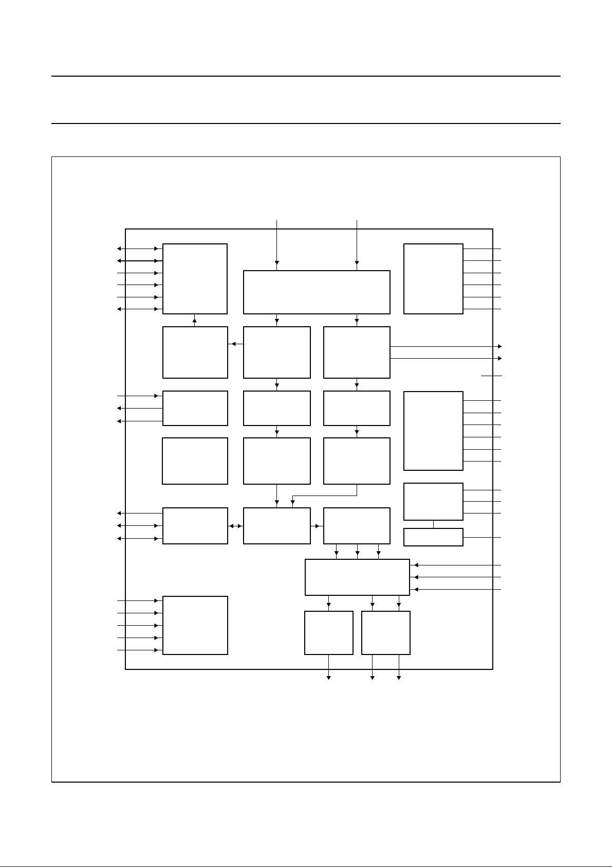
4 BLOCK DIAGRAM
handbook, full pagewidth
P1
P2
ADDR1
ADDR2
SCL
SDA
XTALI
XTALO
SYSCLK
SDO
WS
SCK
41 (37)
4 (42)
18 (13)
23 (19)
33 (29)
34 (30)
20 (15)
19 (14)
38 (34)
35 (31)
36 (32)
37 (33)
2
C-BUS
I
INTERFACE
IDENTIFICATION
CLOCK
PEAK
DETECTION
I2S-BUS
INTERFACE
SIF2
27 (23)
INPUT SWITCH
FM/AM
DEMODULATION
DEMATRIX
2-CHANNEL
ANALOG/
SATELLITE
DECODER
DIGITAL
SELECTOR
AGC, ADC
DEMODULATION
SIF1
29 (25)
NICAM
NICAM
DECODER
LEVEL
ADJUST
POST FILTER
3 DACs
SUPPLY
SIF
DIGITAL
SUPPLY
SUPPLY
DACs
OPAMPS
REFERENCE
(21) 25
(20) 24
(28) 32
(27) 31
(24) 28
(18) 22
(10) 15
(12) 17
(8)
(7) 13
(6) 12
(5) 11
(35) 39
(36) 40
(26) 30
(3) 9
(4) 10
(44) 6
(41) 3
V
DEC
V
SSA2
V
DDA3
V
SSA3
V
ref1
I
ref
NICAM
PCLK
n.c.
V
SSD2
V
DDD1
V
SSD1
V
DDD3
V
SSD3
CRESET
V
DDA1
V
SSA1
V
SSA4
V
ref2
TDA9874APS
(TDA9874AH)
TP1
TP2
TP3
26 (22)
21 (17)
16 (11)
14 (9)
(16)
TEST
TEST1
TEST2
The pin numbers given in parenthesis refer to the TDA9874AH.
Fig.1 Block diagram.
2000 Aug 04 6
CROSSBAR
MONO
CHANNEL
OUTPUT
BUFFERS
5 (43)
OUTM
ANALOG
SWITCH
OUTL OUTR
2-CHANNEL
OUTPUT
BUFFERS
7 (1) 8 (2)
(39) 1
(40) 2
(38) 42
MHB584
EXTIR
EXTIL
MONOIN
Page 7

Philips Semiconductors Product specification
Digital TV sound demodulator/decoder TDA9874A
5 PINNING
SYMBOL
DESCRIPTION
SDIP42 QFP44
EXTIR 1 39 external audio input right channel
EXTIL 2 40 external audio input left channel
PIN
V
ref2
3 41 analog reference voltage for DAC and operational amplifiers
P2 4 42 second general purpose I/O pin
OUTM 5 43 analog output mono
V
SSA4
6 44 analog ground supply 4 for analog back-end circuitry
OUTL 7 1 analog output left
OUTR 8 2 analog output right
V
V
V
V
V
DDA1
SSA1
SSD1
DDD1
SSD2
9 3 analog supply voltage 1; back-end circuitry 5 V
10 4 analog ground supply 1; back-end circuitry
11 5 digital ground supply 1; core circuitry
12 6 digital supply voltage 1; core voltage regulator circuitry
13 7 digital ground supply 2; core circuitry
n.c. − 8 not connected
TP2 14 9 additional test pin 2; connected to V
SSD
NICAM 15 10 serial NICAM data output (at 728 kHz)
TP1 16 11 additional test pin 1; connected to V
SSD
PCLK 17 12 NICAM clock output (at 728 kHz)
ADDR1 18 13 first I
2
C-bus slave address modifier input
XTALO 19 14 crystal oscillator output
XTALI 20 15 crystal oscillator input
TP3 − 16 additional test pin 3; connected to V
TEST2 21 17 test pin 2; connected to V
I
ref
ADDR2 23 19 second I
V
SSA2
V
DEC
22 18 resistor for reference current generation; front-end circuitry
2
C-bus slave address modifier input
24 20 analog ground supply 2; analog front-end circuitry
25 21 analog front-end circuitry supply voltage decoupling
TEST1 26 22 test pin 1; connected to V
SSD
SSD
SSD
for normal operation
for normal operation
SIF2 27 23 sound IF input 2
V
ref1
28 24 reference voltage; for analog front-end circuitry
SIF1 29 25 sound IF input 1
CRESET 30 26 capacitor for Power-on reset
V
SSA3
V
DDA3
SCL 33 29 I
SDA 34 30 I
SDO 35 31 I
WS 36 32 I
31 27 digital ground supply 3; front-end circuitry
32 28 analog front-end circuitry regulator supply voltage 3 (5 V)
2
C-bus serial clock input
2
C-bus serial data input/output
2
S-bus serial data output
2
S-bus word select input/output
for normal operation
for normal operation
for normal operation
2000 Aug 04 7
Page 8
Philips Semiconductors Product specification
Digital TV sound demodulator/decoder TDA9874A
SYMBOL
PIN
SDIP42 QFP44
SCK 37 33 I2S-bus clock input/output
SYSCLK 38 34 system clock output
V
V
DDD3
SSD3
39 35 digital supply voltage 3; digital I/O pads
40 36 digital ground supply 3; digital I/O pads
P1 41 37 first general purpose I/O pin
MONOIN 42 38 analog mono input
handbook, halfpage
V
V
V
V
ADDR1
XTALO
EXTIR
EXTIL
V
ref2
P2
OUTM
V
SSA4
OUTL
OUTR
DDA1
V
SSA1
SSD1
DDD1
SSD2
TP2
NICAM
TP1
PCLK
XTALI
TEST2
1
2
3
4
5
6
7
8
9
10
11
TDA9874APS
12
13
14
15
16
17
18
19
20
MHB585
42
41
40
39
38
37
36
35
34
33
32
31
30
29
28
27
26
25
24
23
2221
MONOIN
P1
V
V
SYSCLK
SCK
WS
SDO
SDA
SCL
V
V
CRESET
SIF1
V
SIF2
TEST1
V
V
ADDR2
I
ref
DESCRIPTION
SSD3
DDD3
DDA3
SSA3
ref1
DEC
SSA2
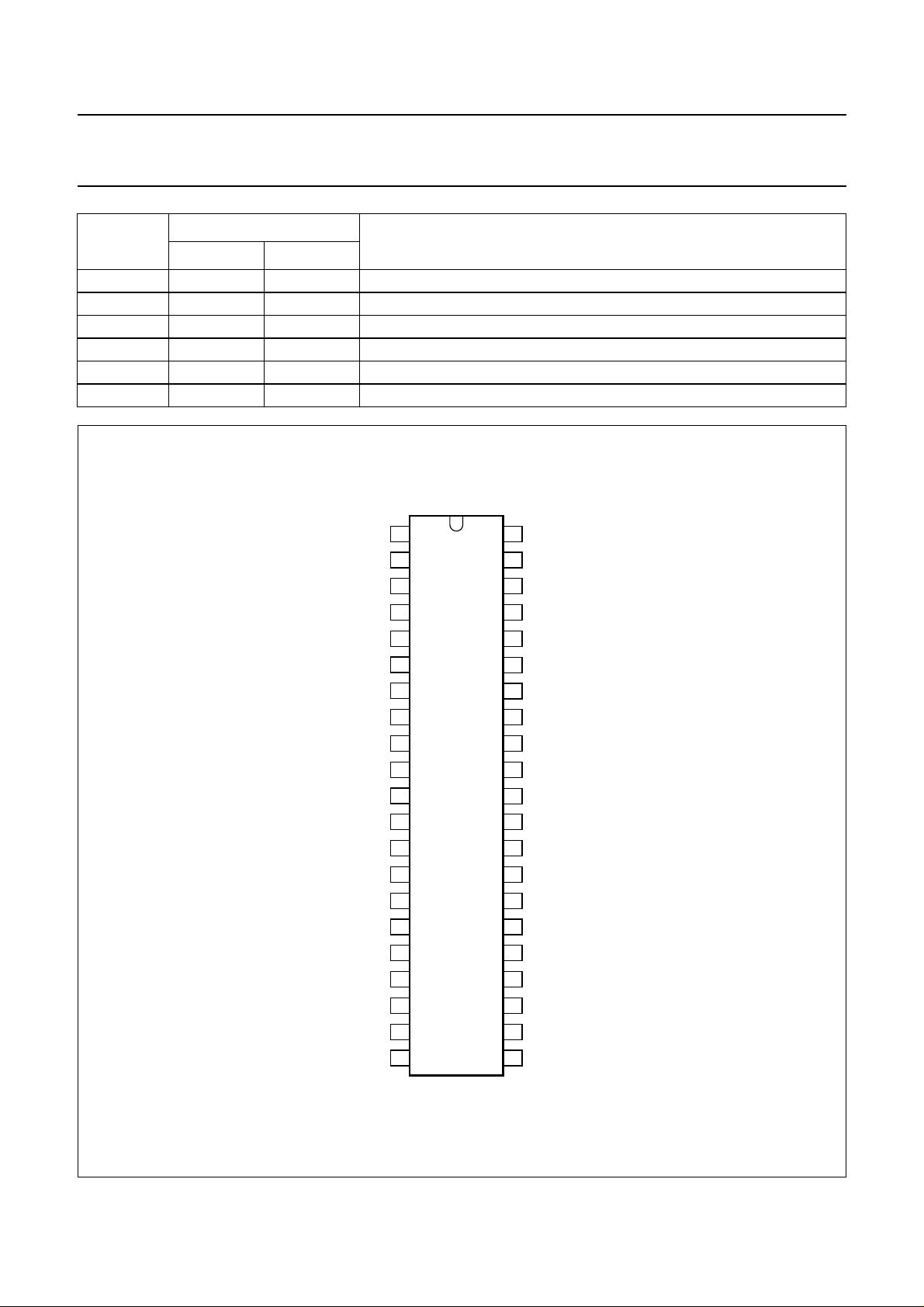
Fig.2 Pin configuration (SDIP42).
2000 Aug 04 8
Page 9
Philips Semiconductors Product specification
Digital TV sound demodulator/decoder TDA9874A
handbook, full pagewidth
OUTL
OUTR
V
DDA1
V
SSA1
V
SSD1
V
DDD1
V
SSD2
n.c.
TP2
NICAM
TP1
P2
42
14
XTALO
ADDR1
ref2
V
EXTIL
EXTIR
41
40
39
TDA9874AH
15
16
17
TP3
XTALI
TEST2
I
SSA4
V
OUTM
44
43
1
2
3
4
5
6
7
8
9
10
11
12
13
PCLK
P1
MONOIN
38
37
18
19
ref
ADDR2
SSD3
V
36
20
SSA2
V
DDD3
V
35
21
DEC
V
SYSCLK
34
22
TEST1
33
32
31
30
29
28
27
26
25
24
23
MHB586
SCK
WS
SDO
SDA
SCL
V
DDA3
V
SSA3
CRESET
SIF1
V
ref1
SIF2
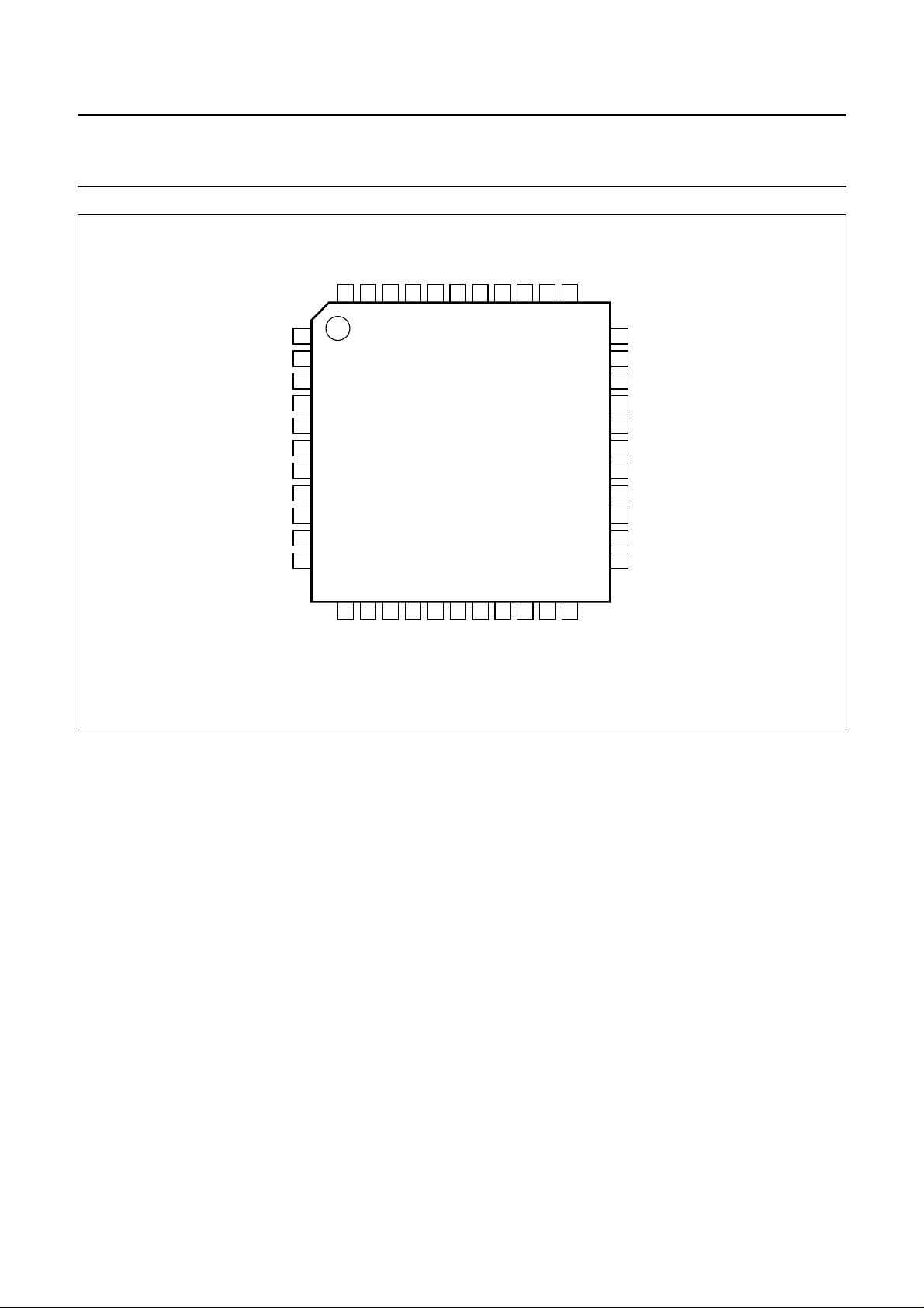
Fig.3 Pin configuration (QFP44).
6 FUNCTIONAL DESCRIPTION
6.1 Description of the demodulator and decoder section
6.1.1 SIF INPUTS
Twoinputsareprovided,pin SIF1andpin SIF2. For higher
SIF signal levels the SIF input can be attenuated with an
internal switchable −10 dB resistor divider. As no specific
filters are integrated, both inputs have the same
specification giving flexibility in application. The selected
signal is passed through an AGC circuit and then digitized
by an 8-bit ADC operating at 24.576 MHz.
6.1.2 AGC
The gain of the AGC amplifier is controlled from the ADC
output by means of a digital control loop employing
hysteresis. The AGC has a fast attack behaviour to
prevent ADC overloads, and a slow decay behaviour to
prevent AGC oscillations. For AM demodulation the AGC
must be switched off. When switched off, the control loop
is reset and fixed gain settings can be chosen
(see Table 14).
The AGC can be controlled via the I2C-bus; details are
given in Sections 7.3.2, 7.3.3 and 7.4.6.
6.1.3 MIXER
The digitized input signal is fed to the mixers, which mix
one or both input sound carriers down to zero IF. A 24-bit
control word for each carrier sets the required frequency.
Access to the mixer control word registers is via the
I2C-bus (see Sections 7.3.5 and 7.3.6) or via Easy
Standard Programming (ESP, see Section 7.3.23). When
receiving NICAM programs, a feedback signal is added to
the control word of the second carrier mixer to establish a
carrier-frequency loop.
6.1.4 FM AND AM DEMODULATION
An FM or AM input signal is fed through a switchable
band-limiting filter into a demodulator that can be used for
either FM or AM demodulation. Apart from the standard
(fixed) de-emphasis characteristic, an adaptive
de-emphasis is available for Wegener-Panda 1 encoded
satellite programs.
2000 Aug 04 9
Page 10

Philips Semiconductors Product specification
Digital TV sound demodulator/decoder TDA9874A
6.1.5 FM DECODING
A2-carrierstereodecoderrecoverstheleft and right signal
channels from the demodulated sound carriers. Both the
European and Korean stereo systems are supported.
AutomaticFM dematrixing is also supported,whichmeans
that the FM sound mode identification (mono, stereo or
dual) switches the FM dematrix directly. No loop via the
microcontroller is needed.
For highly overmodulated signals, a high deviation mode
for monaural audio sound single carrier demodulation can
be selected.
NICAM decoding is still possible in high deviation mode.
6.1.6 FM IDENTIFICATION
The identification of the FM sound mode is performed by
AM synchronous demodulation of the pilot and
narrow-band detection of the identification frequencies.
Theresultisavailableviathe I2C-businterface.Aselection
can be made via the I2C-bus for B/G, D/K and M
standards, and for three different time constants that
representdifferenttrade-offsbetweenspeedandreliability
ofidentification.Apilotdetectorallowsthecontrolsoftware
to identify an analog 2-carrier (A2) transmission within
approximately 0.1 s.
Automatic FM dematrixing, depending on the
identification, is possible.
6.1.7 NICAM DEMODULATION
The NICAM signal is transmitted in a DQPSK code at a bit
rate of 728 kbits/s. The NICAM demodulator performs
DQPSK demodulation and passes the resulting bitstream
and clock signal to the NICAM decoder and, for evaluation
purposes, to various pins.
Atimingloopcontrolsthefrequencyof the crystal oscillator
to lock the sampling instants to the symbol timing of the
NICAM data.
6.1.8 NICAM DECODING
The device performs all decoding functions in accordance
with the
the frame alignment word, the data is descrambled by
applying the defined pseudo-random binary sequence.
The device then synchronizes to the periodic frame flag
bit C0.
“EBU NICAM 728 specification”
. After locking to
The status of the NICAM decoder can be read outfrom the
NICAMstatusregisterbytheuser(seeSection 7.4.2). The
OSB bit indicates that the decoder has locked to the
NICAM data. The VDSP bit indicates that the decoder has
locked to the NICAM data and that the data is valid sound
data. The C4 bit indicates that the sound conveyed by the
FM mono channel is identical to the sound conveyed by
the NICAM channel.
Theerrorbytecontainsthe number of soundsampleerrors
(resulting from parity checking) that occurred in the past
128 msperiod.TheBitErrorRate(BER)canbecalculated
using the following equation:
BER
6.1.9 NICAM AUTO-MUTE
This function is enabled by setting bit AMUTE to logic 0
(see Section 7.3.12). Upper and lower error limits may be
definedbywritingappropriatevaluestotwo registers in the
I2C-bus section (see Sections 7.3.14 and 7.3.15). When
thenumberoferrorsina128 ms period exceeds the upper
error limit, the auto-mute function will switch the output
sound from NICAM to whatever sound is on the first sound
carrier (FM or AM) or to the analog mono input. When the
error count is smaller than the lower error limit, the NICAM
sound is restored.
The auto-mute function can be disabled by setting
bit AMUTE to logic 1. In this case clicks become audible
when the error count increases. The user will hear a signal
of degrading quality.
If no NICAM sound is received, the outputs are switched
from the NICAM channel to the 1st sound carrier.
A decision to enable or disable the auto-mute is taken by
the microprocessor based on an interpretation of the
application control bits C1, C2, C3 and C4, and possibly
any additional strategy implemented by the user in the
microcontroller software.
When the AM sound in NICAM L systems is demodulated
in the 1st sound IF and the audio signal connected to the
mono input of the TDA9874A, the controlling
microprocessor has to ensure switching from NICAM
receptiontomonoinput,ifauto-mutingisdesired.Thiscan
be achieved by setting bit AMSEL = 1 and bit AMUTE = 0.
bit errors
----------------------total bits
error byte 1.74× 10
5–
×≈=
2000 Aug 04 10
Page 11
Philips Semiconductors Product specification
Digital TV sound demodulator/decoder TDA9874A
6.1.10 CRYSTAL OSCILLATOR
The digital controlled crystal oscillator (DCXO) is fully
integrated. Only an external 24.576 MHz crystal is
required.
6.1.11 TEST PINS
All test pins are active HIGH. In normal operation of the
device they can be left open-circuit, as they have internal
pull-down resistors. Test functions are for manufacturing
tests only and are not available to customers.
6.1.12 POWER FAIL DETECTOR
The power fail detector monitors the internal power supply
for the digital part of the device. If the supply has
temporarily been lower than the specified lower limit, the
power failure register bit PFR in subaddress 0 (see
Section 7.4.1), will be set to logic 1. Bit CLRPFR, slave
register subaddress 1 (see Section 7.3.3), resets the
Power-on reset flip-flop to logic 0. If this is detected, an
initialization of the TDA9874A has to be performed to
ensure reliable operation.
6.1.13 POWER-ON RESET
The reset is active LOW. In order to perform a reset at
power-up, a simple RC circuit may be used which consists
of an integrated passive pull-up resistor and an external
capacitor connected to ground. The pull-up resistor has a
nominal value of 50 kΩ, which can easily be measured
between pins CRESET and V
. Before the supply
DDD3
voltage has reached a certain minimum level, the state of
the circuit is completely undefined and remains in this
undefined state until a reset is applied.
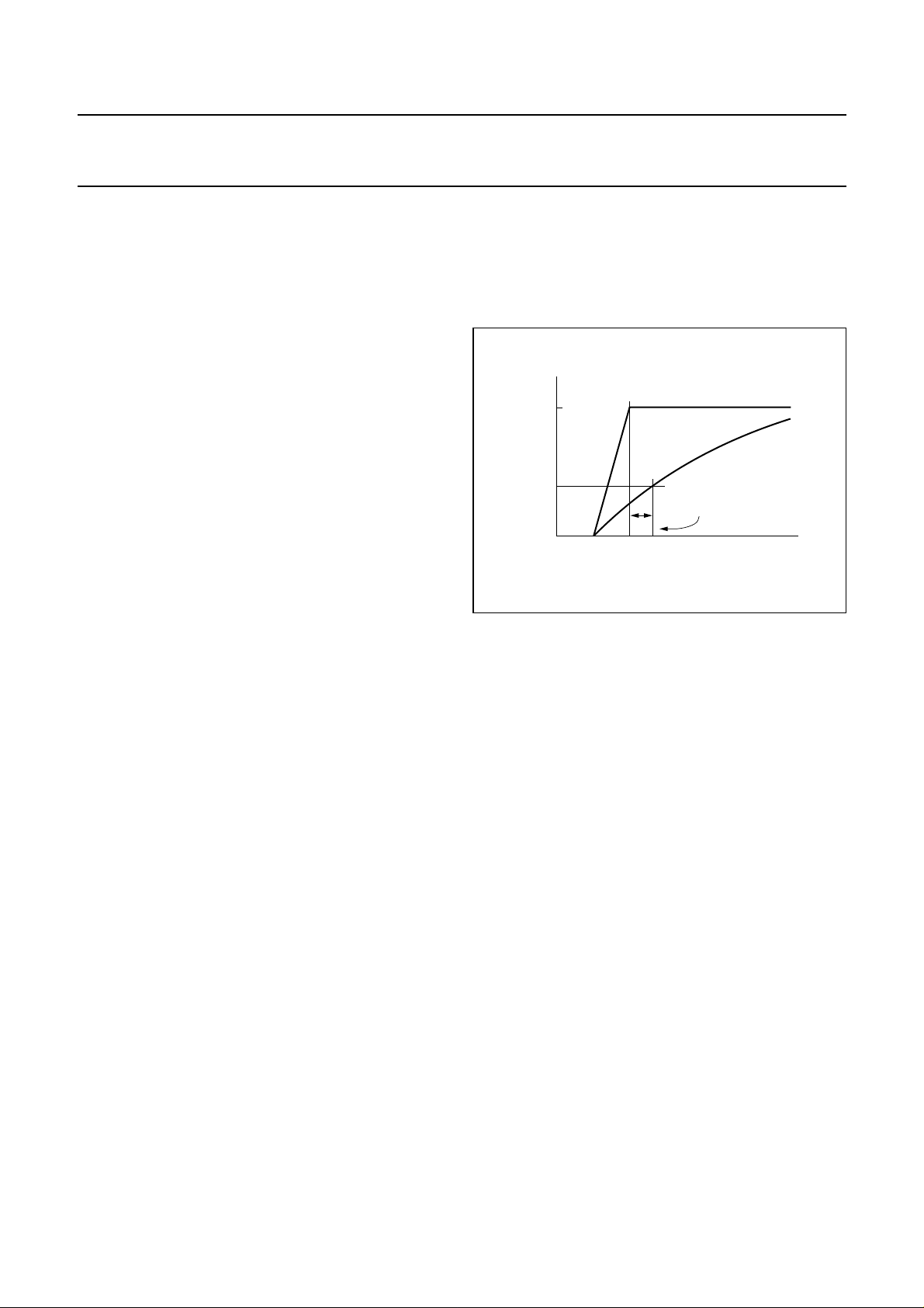
The reset is guaranteed to be active when:
• The power supply is within the specified limits
(4.5 to 5.5 V)
• The crystal oscillator (DCXO) is functioning
• The voltage at pin CRESET is below 0.3V
V
= 5.0 V, typically below 1.8 V).
DDD
DDD
(1.5 V if
The required capacitor value depends on the gradient of
the rising power supply voltage. The time constant of the
RC circuit should be clearly larger than the rise time of the
power supply [to make sure that the reset condition is
always satisfied (see Fig.4)], even when considering
tolerance spreading. To avoid problems with a too slow
discharging of the capacitor at power-down, it may be
helpful to add a diode from pin CRESET to V
DDD
.
It should be noted that the internal ESD protection diode
does not help here as it only conducts at higher voltages.
Under difficult power supply conditions (e.g. very slow or
non-monotonic ramp-up), it is recommended to drive the
reset line from a microcontroller port or the like.
handbook, halfpage
V
5
1.5
V
DDD
> 4.5 V
V
CRESET
reset active
guaranteed
MHB587
< 0.3V
DDD
t
Fig.4 Reset at Power-on.
6.2 Description of the DSP
6.2.1 LEVEL SCALING
All input channels to the digital crossbar switch are
equipped with a level adjustment facility to change the
signal level in a range of ±15 dB. Adjusting the signal level
is intended to compensate for the different modulation
parameters of the various TV standards. Under nominal
conditions it is recommended to scale all input channels to
be 15 dB below full-scale. This will create sufficient
headroom to cope with overmodulation and avoids
changes of the volume impression when switching from
FM to NICAM or vice versa.
6.2.2 NICAM PATH
The NICAM path has a switchable J17 de-emphasis.
6.2.3 NICAM AUTO-MUTE
If NICAM is received, the auto-mute is enabled and the
signalqualitybecomes poor. The digital crossbar switches
automatically to FM, channel 1 or the analog mono input,
as selected by bit AMSEL. This automatic switching
depends on the NICAM bit error rate. The auto-mute
function can be disabled via the I2C-bus.
2000 Aug 04 11
Page 12

Philips Semiconductors Product specification
Digital TV sound demodulator/decoder TDA9874A
6.2.4 FM (AM) PATH
A high-pass filter suppresses DC offsets from the
FM demodulator that may occur due to carrier frequency
offsets, and supplies the FM monitor function with DC
values, e.g. for the purpose of microprocessor controlled
carrier search or fine tuning functions.
An adaptive de-emphasis is available for
Wegener-Panda 1 encoded satellite programs.
The de-emphasis stage offers a choice of settings for the
supported TV standards.
The 2-channel decoder performs the dematrixing of
1
⁄2(L + R), R to L and R signals of1⁄2(L + R) and1⁄2(L − R)
to L and R signals or of channel 1 and channel 2 to
L and R signals, as demanded by the different TV
standards or user preferences.
Automatic FM dematrixing is also supported.
Using the high deviation mode, only channel 1 (mono) can
be demodulated. The scaling is −6 dB compared to
2-channel decoding.
6.2.5 MONITOR
This function provides data words from the
FM demodulator outputs and FM and NICAM signals for
external use, such as carrier search or fine tuning.
The peak level of these signals can also be observed.
Source selection and data read out are performed via the
I2C-bus.
6.2.6 DIGITAL CROSSBAR SWITCH
The input channels are derived from the FM and NICAM
paths,while the output channels comprise I2S-bus and the
audio DACs to the analog crossbar switch. It should be
noted that there is no connection from the external analog
audio inputs to the digital crossbar switch.
6.2.7 DIGITAL AUDIO OUTPUT
The digital audio output interface comprises an I2S-bus
output port and a system clock output. The I2S-bus port is
equipped with a level adjustment facility that can change
the signal level in a ±15 dB range in 1 dB steps. Muting is
possible,too,andoutputscan be disabled toimproveEMC
performance.
TheI2S-busoutputmatrixprovidesthe functions for forced
mono, stereo, channel swap, channel 1 or channel 2.
Automatic selection for TV applications is possible. In this
case the microcontroller program only has to provide a
user controlled sound A or sound B selection.
6.2.8 STEREO CHANNEL TO THE ANALOG CROSSBAR PATH
A level adjustment function is provided with control
positions of 0 dB, +3 dB, +6 dB and +9 dB in combination
with the audio DACs. The Automatic Volume Level (AVL)
function provides a constant output level of
−20 dB (full-scale) for input levels between
0 dB (full-scale) and −26 dB (full-scale). There are some
fixed decay time constants to choose from, i.e.
2, 4 or 8 seconds.
Automatic selection for TV applications is possible. In this
case the microcontroller program only has to provide a
user controlled sound A or sound B selection.
6.2.9 GENERAL
The level adjustment functions can provide signal gain at
multiple locations. Great care has to be taken when using
gain with large input signals, e.g., due to overmodulation,
inorder not to exceed the maximum possible signal swing,
which would cause severe signal distortion. The nominal
signal level of the various signal sources to the digital
crossbar switch should be 15 dB below digital full-scale
(−15 dB full-scale).
2000 Aug 04 12
Page 13
This text is here in white to force landscape pages to be rotated correctly when browsing through the pdf in the Acrobat reader.This text is here in
_white to force landscape pages to be rotated correctly when browsing through the pdf in the Acrobat reader.This text is here inThis text is here in
white to force landscape pages to be rotated correctly when browsing through the pdf in the Acrobat reader. white to force landscape pages to be ...
2000 Aug 04 13
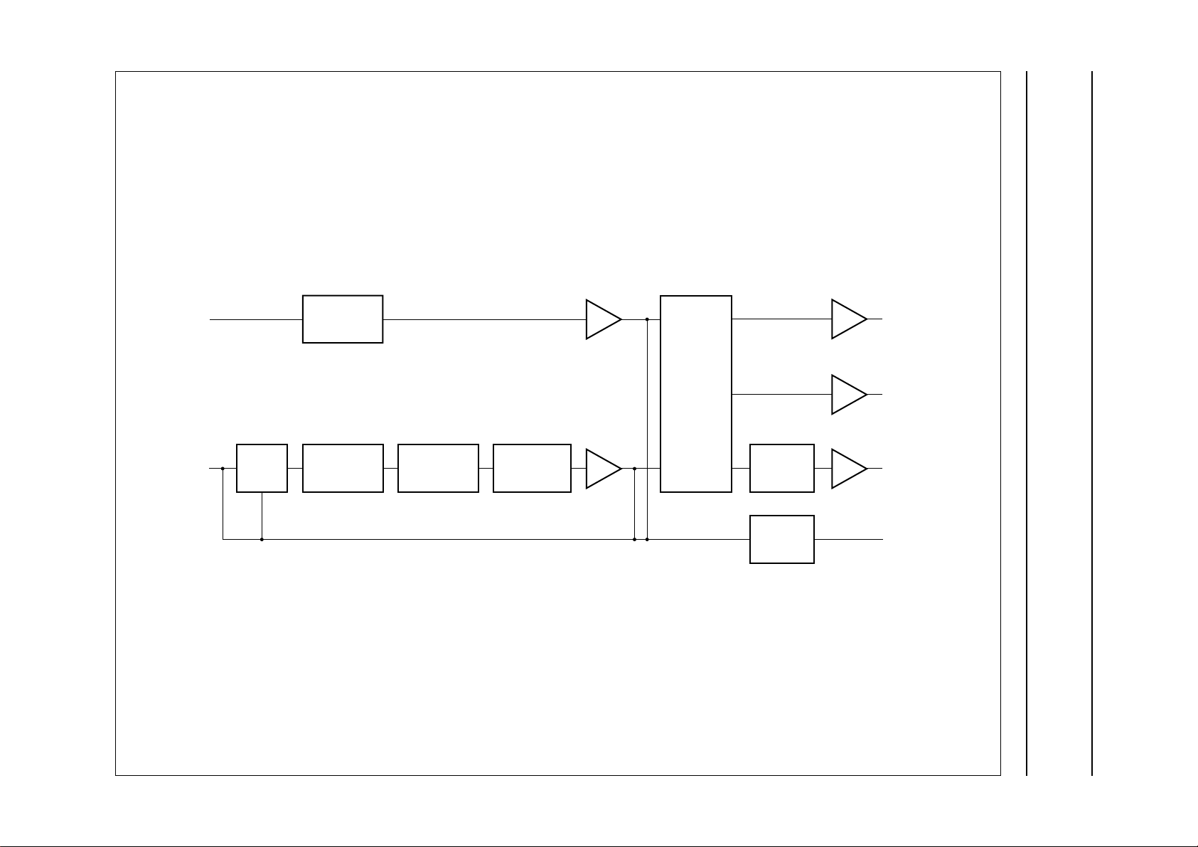
handbook, full pagewidth
Philips Semiconductors Product specification
Digital TV sound demodulator/decoder TDA9874A
NICAM
FM
DC
FILTER
FIXED
DE-EMPHASIS
ADAPTIVE
DE-EMPHASIS
FIXED
DE-EMPHASIS
2-CHANNEL
DECODER
LEVEL
ADJUST
LEVEL
ADJUST
DIGITAL
CROSSBAR
SELECT
MATRIX
MONITOR
LEVEL
ADJUST
LEVEL
ADJUST
LEVEL
ADJUST
stereo DACs
mono DAC
2
I
S-bus
2
C-bus
I
MHB588
Fig.5 DSP data flow diagram.
Page 14
Philips Semiconductors Product specification
Digital TV sound demodulator/decoder TDA9874A
6.3 Description of the analog audio section
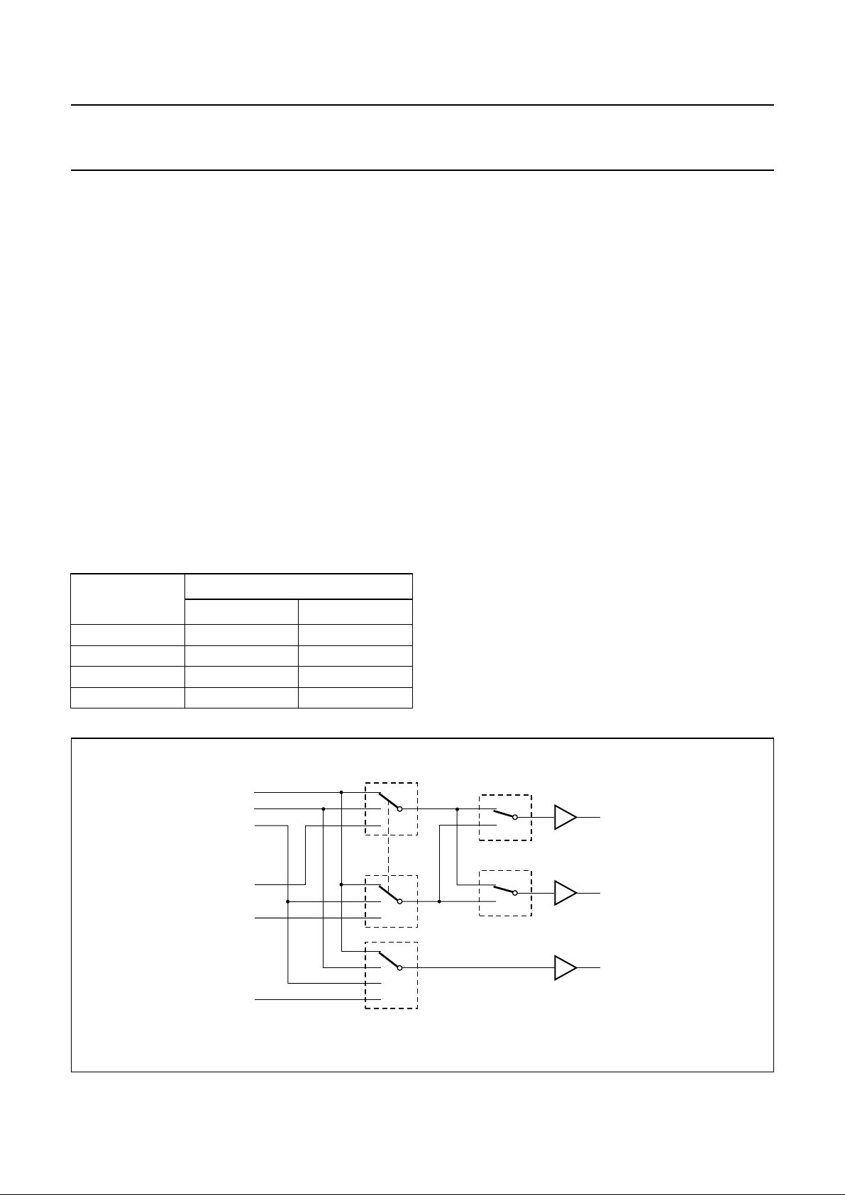
6.3.1 ANALOG CROSSBAR SWITCH AND ANALOG MATRIX
The TDA9874A has one external analog stereo input, one
mono input, one 2-channel and one single-channel output
port. Analog source selector switches are employed to
provide the desired analog signal routing capability, which
is done by the analog crossbar switch section.
The basic signal routing philosophy of the TDA9874A is
that each switch handles two signal channels at the same
time (e.g. left and right, language A and B) directly at the
source. For an overview of the signal flow see Fig.7.
Each source selector switch is followed by an analog
matrix to perform further selection tasks, such as putting a
signal from one input channel, say language A, to both
output channels or for swapping left and right channels.
The analog matrix provides the functions given in Table 5.
Automatic matrixing for TV applications is also supported.
All switches and matrices are controlled via the I2C-bus.
Table 5 Analog matrix functions
MATRIX OUTPUT
MODE
L OUTPUT R OUTPUT
1 L input R input
2 R input L input
3 L input L input
4 R input R input
6.3.2 EXTERNAL AND MONO INPUTS
The external and mono inputs accept signal levels of up to
1.4 V (RMS). By adding external series resistors to
provide suitable attenuation, the external input could be
used as a SCART input. Whenever the external or mono
input is selected, the output of the DAC is muted to
improve the crosstalk performance.
6.3.3 AUDIO DACS
The TDA9874A comprises a 2-channel audio DAC and an
additional single-channel audio DAC for feeding signals
fromtheDSPsectiontotheanalogcrossbarswitch.These
DACs have a resolution of 15 bits and employ four-times
oversampling and noise shaping.
6.3.4 AUDIO OUTPUT BUFFERS
The output buffers provide a gain of 0 dB and offer a
muting possibility. The post filter capacitors of the audio
DACs are connected to the buffer outputs.
6.3.5 STANDBY MODE
The standby mode (see Section 7.3.3) disables most
functions and reduces power dissipation of the
TDA9874A. It provides no other function.
Internal registers may lose their information in standby
mode. Therefore, the device needs to be initialized on
returningtonormaloperation.Thiscan be accomplished in
the same way as after a Power-on reset.
handbook, full pagewidth
mono (AM)
EXTIL
EXTIR
DACL
DACR
DACM
source select
Fig.6 Switch diagram for the analog audio section.
2000 Aug 04 14
matrix
OUTL
OUTR
OUTM
MHB589
Page 15
This text is here in white to force landscape pages to be rotated correctly when browsing through the pdf in the Acrobat reader.This text is here in
_white to force landscape pages to be rotated correctly when browsing through the pdf in the Acrobat reader.This text is here inThis text is here in
white to force landscape pages to be rotated correctly when browsing through the pdf in the Acrobat reader. white to force landscape pages to be ...
2000 Aug 04 15
mono
external
NICAM
FM/AM
NICAM
DEMODULATOR
FM/AM
DEMODULATOR
NICAM
DECODER
ADAPTIVE
DE-EMPHASIS
DE-EMPHASIS
FIXED
DE-EMPHASIS
2-CHANNEL
DECODER
handbook, full pagewidth
LEVEL
ADJUST
LEVEL
ADJUST
DIGITAL
CROSSBAR
SELECT
LEVEL
ADJUST
AVL
DACs
ANALOG
CROSSBAR
SWITCH
MATRIX
MATRIX
MATRIX
BUFFER
BUFFER
LEVEL
ADJUST
STEREO
OUTPUT
MONO
OUTPUT
2
I
S-bus
Philips Semiconductors Product specification
Digital TV sound demodulator/decoder TDA9874A
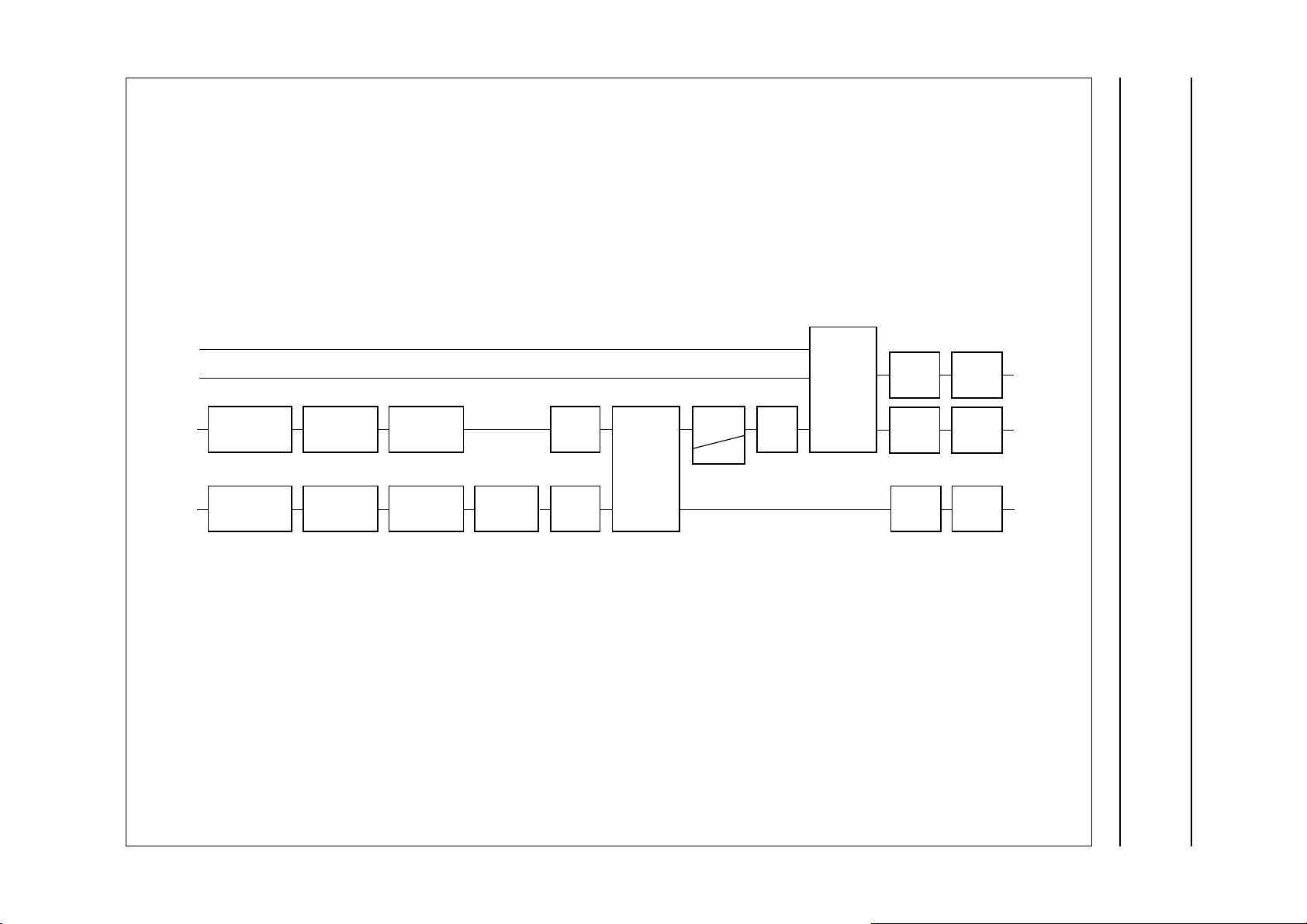
Fig.7 Audio signal flow.
MHB590
Page 16

Philips Semiconductors Product specification
Digital TV sound demodulator/decoder TDA9874A
7I2C-BUS CONTROL
7.1 Introduction
The TDA9874A is controlled only via the I2C-bus. Control
is exercised by writing data to one or more internal
registers. Status information can be read from an array of
registers to let the controlling microprocessor determine
whether any action is required.
The device has an I2C-bus slave transceiver in
accordance with the fast-mode specification with a
maximum speed of 400 kbits/s. Information about the
I2C-bus can be found in brochure
it”
(order number 9398 393 40011). To avoid conflicts in a
real application with other ICs providing similar or
complementing functions, there are four possible slave
addresses available, which can be selected by
pins ADDR1 and ADDR2 (see Table 6).
Table 6 Possible slave addresses
ADDR2 ADDR1
0 0 1011000
0 1 1011001
1 0 1011010
1 1 1011011
The I2C-bus interface remains operational in the standby
mode of the TDA9874A to allow the device to be
reactivated via the I2C-bus.
The device will not respond to a ‘general call’ on the
I2C-bus, i.e. when a slave address of 0000 000 is sent by
a master.
A6 A5 A4 A3 A2 A1 A0
“I2C-bus and how to use
SLAVE ADDRESS
7.2 Power-up state
After Power-on reset respectively at power-up the device
is in the following state:
• All outputs muted
• No sound carrier frequency loaded
• General purpose I/O pins ready for input (HIGH)
• Input SIF1 selected with:
– AGC on
– SIF 10 dB attenuator off
– Small hysteresis.
• Demodulators for both sound carriers set to FM with:
– Identification for B/G, D/K, identification mode ‘slow’
– Level adjustment set to 0 dB
– De-emphasis 50 µs
– Dematrix set to mono
– Adaptive de-emphasis off.
• Analog outputs are muted and connected to DACs
• Digital audio interface all outputs off
• Monitor set to carrier 1 DC output.
After Power-on reset or power-up, a device initialization
has to be performed via the I
into the proper mode of operation, in accordance with the
desired TV standard, etc. This can be done by writing to all
registers with a single I2C-bus transmission (such as a
refresh operation) or by writing selectively only to those
registers, the contents of which need to be changed with
regardtothepower-upstate. Easy StandardProgramming
(ESP) can also be used.
2
C-bus to put the TDA9874A
2000 Aug 04 16
Page 17

Philips Semiconductors Product specification
Digital TV sound demodulator/decoder TDA9874A
7.3 Slave receiver mode
As a slave receiver, the TDA9874A provides 26 registers
for storing commands and data. Each register is accessed
via a so-called subaddress. A subaddress can be thought
of as a pointer to an internal memory location.
Detailed descriptions of the slave receiver registers are
given in Sections 7.3.2 to 7.3.21.
It is allowed to send more than one data byte per
transmission to the TDA9874A. In this event, the
subaddress is automatically incremented after each data
byte, resulting in storing the sequence of data bytes at
successive register locations, starting at SUBADDRESS.
A transmission can start at any valid subaddress. Each
byte that is properly stored, is acknowledged with
A (acknowledge).
2
Table 7 I
S SLAVE ADDRESS 0 A SUBADDRESS A DATA A P
Table 8 Explanation of Table 7
C-bus; slave address, subaddress, data format
If an attempt is made to write data to a non-existing
subaddress, the device acknowledges with A (not
acknowledge),thereforetellingtheI2C-busmastertoabort
the transmission. There is no ‘wrap-around’ of
subaddresses.
Commands and data will be processed as soon as they
have been received completely. Functions requiring more
than one byte will thus be executed only after all bytes for
that function have been received. If the transmission is
terminated (STOP condition) before all bytes have been
received, the incomplete data for that function is ignored.
Data patterns sent to the various subaddresses are not
checked for being illegal or not at that address, except for
the level adjustment functions.
Detection of a STOP condition without a preceding
acknowledge bit is regarded as a bus error. In this case,
the last operation will not be executed.
BIT FUNCTION
S START condition
SLAVE ADDRESS 7-bit device address
0 data direction bit (write to device)
A acknowledge
SUBADDRESS address of register to write to
DATA data byte to be written into register
P STOP condition
Table 9 Format for a transmission employing auto-increment of subaddresses
S SLAVE ADDRESS 0 A SUBADDRESS A DATA
BYTE A
Note
1. n data bytes with auto-increment of subaddresses.
7.3.1 PROGRAMMING VIA THE I2C-BUS
The TDA9874A can be programmed in the same way as
its predecessor (TDA9874H) using the
subaddresses 0 to 24 or by using ESP.
7.3.1.1 Programming via subaddresses 0 to 24
While programming the TDA9874A, by writing to
subaddresses 0 to 24, it is not allowed to access
subaddress 255. Writing data to subaddress 255 will
overwrite the data previously written to subaddresses
3 to 10. This may cause unwanted effects.
DATA A P
(1)
2000 Aug 04 17
Page 18

Philips Semiconductors Product specification
Digital TV sound demodulator/decoder TDA9874A
7.3.1.2 Using Easy Standard Programming (ESP)
This facility simplifies programming by reducing the
amount of data to be set-up and transferred via the
I2C-bus.
Subaddress 255givescontrolof most standarddependent
settings of the IC; see ESP register in Section 7.3.23.
When using ESP it is recommended not to write data to
subaddresses 3 to 10.
A possible programming flow for using ESP and automatic
FM dematrixing (bit TVSM = 1 and bit IDSWFM = 1) is
shown in Table 10. It should be noted that the NICAM
configurationregisterandtheleveladjustmentregistersfor
FM and NICAM are not affected by ESP.
Table 10 Programming the TDA9874A by using ESP and automatic FM dematrixing
REGISTER
CONTENT OF REGISTER
NUMBER NAME
0 AGCGR Set AGCGR = 20H for using the −10 dB attenuator at the SIF input, otherwise write a 00H to
this register.
1 GCONR Select the chosen SIF input pin by writing data to bit SIFSEL (bit 0) and choose the AGC
decay time corresponding to your application by writing the appropriate data to
bit AGCSLOW (bit 2).
2 MSR set this register according to your sound mode detection algorithm
3to10 − do NOT write data to these registers while using ESP
11 FMMR set FMMR = 80H to choose automatic FM dematrixing
12 C1OLAR see Table 36
13 C2OLAR see Table 37
14 NCONR set NCONR = 04H to select FM source automatically if NICAM is not available
15 NOLAR see Table 40
16 NLELR set NLELR = 14H (default setting after Power-on reset) if no other value is chosen
17 NUELR set NUELR = 50H (default setting after Power-on reset) if no other value is chosen
18 AMCONR set AMCONR = F9H to enable all analog outputs
19 SDACOSR set SDACOSR = 81H to select +6 dB gain (see Table 46) and NICAM or FM output
20 AOSR To select an internal source set AOSR = 80H to select dual A or set AOSR = C0H to select
dual B (if dual mode is transmitted) to all analog outputs. For selecting an external source
see Section 7.3.18.
21 DAICONR use only for I
2
22 I
23 I
SOSR use only for I2S-bus output, see detailed description in Section 7.3.20
2
SOLAR use only for I2S-bus output, see detailed description in Section 7.3.21
2
S-bus output, see detailed description in Section 7.3.19
24 MDACOSR Set MDACOSR = 82H to select dual A or set MDACOSR = 83H to select dual B (if dual
mode is transmitted) to all analog outputs. For selecting an external source see
Section 7.3.22.
255 ESP see detailed description in Section 7.3.23
2000 Aug 04 18
Page 19

This text is here in white to force landscape pages to be rotated correctly when browsing through the pdf in the Acrobat reader.This text is here in
_white to force landscape pages to be rotated correctly when browsing through the pdf in the Acrobat reader.This text is here inThis text is here in
white to force landscape pages to be rotated correctly when browsing through the pdf in the Acrobat reader. white to force landscape pages to be ...
2000 Aug 04 19
Table 11 Overview of the slave receiver registers
SUBADDRESS
(DECIMAL)
0 0 0 AGCLEV B4 B3 B2 B1 B0 AGC gain selection
1 P2OUT P1OUT STDBY INIT CLRPFR AGCSLOW AGCOFF SIFSEL general configuration
2 PEAK 0 0 MCSM1 MCSM0 0 MSS1 MSS0 monitor select
3 B7 B6 B5 B4 B3 B2 B1 B0 carrier 1 frequency;
4 B7 B6 B5 B4 B3 B2 B1 B0 carrier 1 frequency
5 B7 B6 B5 B4 B3 B2 B1 B0 carrier 1 frequency;
6 B7 B6 B5 B4 B3 B2 B1 B0 carrier 2 frequency;
7 B7 B6 B5 B4 B3 B2 B1 B0 carrier 2 frequency
8 B7 B5 B5 B4 B3 B2 B1 B0 carrier 2 frequency;
9 IDMOD1 IDMOD0 IDAREA FILTBW1 CH2MOD1 CH2MOD0 FILTBW0 CH1MODE demodulator
10 ADEEM2 FMDSC23 FMDSC22 FMDSC21 ADEEM1 FMDSC13 FMDSC12 FMDSC11 FM de-emphasis
11 IDSWFM 0 0 0 0 FDMS2 FDMS1 FDMS0 FM dematrix
12 0 0 0 B4 B3 B2 B1 B0 channel 1 output level
13 0 0 0 B4 B3 B2 B1 B0 channel 2 output level
14 DCXOPULL DCXOTEST 0 DOUTEN 0 AMSEL NDEEM AMUTE NICAM configuration
15 0 0 0 B4 B3 B2 B1 B0 NICAM output level
16 B7 B6 B5 B4 B3 B2 B1 B0 NICAM lower error limit
17 B7 B6 B5 B4 B3 B2 B1 B0 NICAM upper error limit
18 1 MUTI2S 1 1 1 MUTSOUT MUTMOUT 1 audio mute control
19 SDGS1 0 AVL1 AVL0 SDGS0 0 SDOS1 SDOS0 stereo DAC output
20 TVSM CSM2 CSM1 CSM0 MOS1 MOS0 SSS1 SSS0 analog output select
7 6543210
DATA
FUNCTION
(ignored if AGC on)
MS part
LS part
MS part
LS part
configuration
adjustment
adjustment
adjustment
select
Philips Semiconductors Product specification
Digital TV sound demodulator/decoder TDA9874A
Page 20

This text is here in white to force landscape pages to be rotated correctly when browsing through the pdf in the Acrobat reader.This text is here in
_white to force landscape pages to be rotated correctly when browsing through the pdf in the Acrobat reader.This text is here inThis text is here in
white to force landscape pages to be rotated correctly when browsing through the pdf in the Acrobat reader. white to force landscape pages to be ...
2000 Aug 04 20
SUBADDRESS
(DECIMAL)
21 0 0 0 SYSCL1 SYSCL0 SYSOUT I2SFORM IS2OUT digital audio interface
22 TVSMIIS ICSM2 ICSM1 ICSM0 0 0 ISS1 ISS0 I2S-bus output select
23 0 0 0B3B2B1B0B0I
24 MDGS1 0 0 0 MDGS0 0 MDOS1 MDOS0 mono DAC output select
25 0 0 0 0 0 0 0 0 reserved
255 FILTBW1 FILTBW0 IDMOD1 IDMOD0 EPB3 EPB2 EPB1 EPB0 ESP
7 6543210
DATA
FUNCTION
configuration
2
S-bus output level
adjustment
Philips Semiconductors Product specification
Digital TV sound demodulator/decoder TDA9874A
Page 21

Philips Semiconductors Product specification
Digital TV sound demodulator/decoder TDA9874A
7.3.2 AGC GAIN REGISTER (AGCGR)
If the AGC function is switched off in the general
configuration register (see Section 7.3.3), the contents of
thisregisterdefinesafixedgainoftheSIFinputstage.The
input voltages given are meant to generate a nearly
full-scale output from the SIF ADC. If the AGC is on, the
AGC gain setting is ignored. After switching off the AGC
function, the latest gain control setting is copied to the
AGC gain register.
Table 12 AGC gain register (subaddress 0)
76543210
0 0 AGCLEV AGCB4 AGCB3 AGCB2 AGCB1 AGCB0
Table 13 Description of the AGC gain register bits
BIT NAME DESCRIPTION
7 − this bit is not used and should be set to a logic 0
6 − this bit is not used and should be set to a logic 0
5 AGCLEV If the AGC input level shift bit AGCLEV = 1 the input signal is scaled with −10 dB.
Bit AGCLEV is also active if the automatic gain function is enabled.
4 AGCB4 Ifthe automatic gain control function is switched off in the general configuration register,
3 AGCB3
2 AGCB2
1 AGCB1
0 AGCB0
the contents of this register will define a fixed gain of the AGC stage.
If the AGC input level shift bit AGCLEV is set to logic 1 the
input signal is scaled with −10 dB. The bit AGCLEV is also
active if the AGC function is enabled.
The default setting after Power-on reset is 0000 0000.
In Table 14 the stated step number corresponds with the
SIF level read from subaddress 7 (see Section 7.4.6); the
inputvoltagesshouldbeconsideredasapproximate target
values.
2000 Aug 04 21
Page 22

Philips Semiconductors Product specification
Digital TV sound demodulator/decoder TDA9874A
Table 14 AGC gain register
76 5 43210
−−AGCLEV AGCB4 AGCB3 AGCB2 AGCB1 AGCB0
000/111111 0.0 333/1052
000/111110 0.8 304/963
000/111101 1.5 278/881
000/111100 2.3 255/806
000/111011 3.1 233/737
000/111010 3.9 213/674
000/111001 4.6 195/617
000/111000 5.4 178/564
000/110111 6.2 163/516
000/110110 7.0 149/472
000/110101 7.7 136/432
000/110100 8.5 125/395
000/110011 9.3 114/361
000/11001010.1 104/330
000/11000110.8 96/302
000/11000011.6 87/276
000/10111112.4 80/253
000/10111013.2 73/231
000/10110113.9 67/212
000/10110014.7 61/194
000/10101115.5 56/177
000/10101016.3 51/162
000/10100117.0 47/148
000/10100017.8 43/135
000/10011118.6 39/124
000/10011019.4 36/113
000/10010120.1 33/104
000/10010020.9 30/95
000/10001121.7 27/87
000/10001022.5 25/79
000/10000123.2 23/73
000/10000024.0 21/66
AGC GAIN
(dB)
MAX. SIF INPUT
VOLTAGE [mV (RMS)]
2000 Aug 04 22
Page 23

Philips Semiconductors Product specification
Digital TV sound demodulator/decoder TDA9874A
7.3.3 GENERAL CONFIGURATION REGISTER (GCONR)
The default setting after Power-on reset is 1100 0000.
Table 15 General configuration register (subaddress 1)
76543210
P2OUT P1OUT STDBY INIT CLRPFR AGCSLOW AGCOFF SIFSEL
Table 16 Description of the general configuration register bits
BIT SYMBOL DESCRIPTION
7 P2OUT General purpose I/O pins 1 and 2: these bits control the general purpose input/output
6 P1OUT
5 STDBY Standby mode on/off: if bit STDBY = 1 the TDA9874A is set to the standby mode. Most
4 INIT Initialize to default settings: if bit INIT = 1 it causes initialization of the TDA9874A to its
3 CLRPFR Clear power failure register: if bit CLRPFR = 1 it resets the clear power failure register.
2 AGCSLOW AGC decay time: if bit AGCSLOW = 1 a longer decay time and larger hysteresis are
1 AGCOFF AGC on/off: if bit AGCOFF = 1 it forces the AGC block to a fixed gain as defined in the
0 SIFSEL SIFinput select: if bit SIFSEL = 1 it selects pin SIF2 for input (recommended for satellite
pins. The contents of these bits is written directly to the corresponding pins. If an input is
desired, the bits must be set to 1 to allow the pins to be pulled to LOW levels externally.
Input from the pins is reflected in the device status register (see Section 7.4.1).
Bit P1OUT is recommended to be used for switching an SIF trap for the adjacent picture
carrier in designs that employ such a trap.
functions are disabled and power dissipation is somewhat reduced. If bit STDBY = 0 the
TDA9874A is in its normal mode of operation. On return from standby mode, the device
is in its Power-on reset mode and needs to be re-initialized with data defined by the
user.
default settings. This has the same effect as a Power-on reset. In the event of a conflict
between the default settings and any bit set to logic 1 in this register, the bits actually
written to this register will overwrite the default settings. This bit is automatically reset
to 0 after initialization has been completed. When set to logic 0, the TDA9874A is in its
normal mode of operation.
This bit is automatically reset to logic 0 after bit PFR in the device status register has
been read.
selected for input signals with strong video modulation (conventional intercarrier). This
bit has only an effect, If bit AGCOFF = 0. If bit AGCSLOW = 0 it selects normal attack
and decay times for the AGC and a small hysteresis.
AGC gain register (see Section 7.3.2). If bit AGCOFF = 0 the AGC function is enabled
and the contents of the AGC gain register are ignored.
tuner). If bit SIFSEL = 0 it selects pin SIF1 (recommended for terrestrial TV).
2000 Aug 04 23
Page 24

Philips Semiconductors Product specification
Digital TV sound demodulator/decoder TDA9874A
7.3.4 MONITOR SELECT REGISTER (MSR)
This register is used to define the signal source (the level of which is to be monitored) and the signal channel. Data can
be monitored e.g. before or after the DC filter at the FM/AM demodulator outputs. The peak level of signals can also be
observed. The last available data sample can be read out in the I2C-bus slave transmitter mode (see Section 7.4.5).
Phase means the differentiated phase output of the FM demodulator and is provided when the demodulator operates in
FM mode. The magnitude is supplied in AM mode.
The default setting after Power-on reset is 0000 0000.
Table 17 Monitor select register (subaddress 2)
76543210
PEAK 0 0 MCSM1 MCSM0 0 MSS1 MSS0
Table 18 Description of the monitor select register bits
BIT SYMBOL DESCRIPTION
7 PEAK Peak level select: if bit PEAK = 1 it selects the rectified peak level of a source to be
monitored. Peak level value is reset to logic 0 after read-out (see read registers
5 and 6). After changing the monitor signal source for peak calculation it is advisable to
ignore the first read-out value due to stored data from previous calculations.
6 − these bits are not used and should be set to logic 0
5 −
4 MCSM1 Signal channel select: the state of these bits determine which signal channel is
3 MCSM0
2 − this bit is not used and should be set to logic 0
1 MSS1 Signal source select: the state of these bits determine which signal source is selected;
0 MSS0
selected; see Table 19.
see Table 20.
Table 19 Signal channel selection
MCSM1 MCSM0 SIGNAL CHANNEL
00
0 1 CH1
1 0 CH2
Table 20 Signal source selection
MSS1 MSS0 SIGNAL SOURCE
0 0 DC output of FM/AM demodulator
0 1 magnitude/phase output of FM/AM demodulator
1 0 FM/AM path output
1 1 NICAM path output
2000 Aug 04 24
CH1 CH2+
-----------------------------2
Page 25

Philips Semiconductors Product specification
Digital TV sound demodulator/decoder TDA9874A
7.3.5 CARRIER 1 FREQUENCY REGISTER
This register should not be used when applying ESP.
Three bytes are required to define a 24-bit frequency
control word to represent the sound carrier (i.e. mixer)
frequency. These three bytes are stored at
subaddresses 3 to 5; subaddress 3 being the high byte.
Execution of the command starts only after all bytes have
been received. If an error occurs, e.g. a premature STOP
condition, partial data for this function is ignored. The
relation of the sound carrier frequency and the control
word is given in the following formula:
f
data
mix
-------f
clk
224×=
where:
data = 24-bit frequency control word
f
= desired sound carrier frequency
mix
f
= 12288 MHz (clock frequency of mixer)
clk
224= 16777216 (number of steps in a 24-bit word size).
Example: A 5.5 MHz sound carrier frequency will be
generated by sending the following sequence of data
bytes to the TDA9874A (data = 7509333 in decimal
notation or 729555 in hexadecimal notation):
0111 0010 1001 0101 0101 0101.
The default setting after Power-on reset is 0000 0000 for
all three bytes.
Table 21 Carrier 1 frequency register high byte (subaddress 3)
76543210
B7 B6 B5 B4 B3 B2 B1 B0
Table 22 Carrier 1 frequency register middle byte (subaddress 4)
76543210
B7 B6 B5 B4 B3 B2 B1 B0
Table 23 Carrier 1 frequency register low byte (subaddress 5)
76543210
B7 B6 B5 B4 B3 B2 B1 B0
7.3.6 CARRIER 2 FREQUENCY REGISTER
This register should not be used when applying ESP. The
format is the same as for sound carrier 1, except
If this register is used, it will be for either the second
FM sound carrier of a terrestrial or satellite FM program or
for the NICAM sound carrier.
subaddresses 6 to 8 are used. Subaddress 6 holds the
high byte.
2000 Aug 04 25
Page 26

Philips Semiconductors Product specification
Digital TV sound demodulator/decoder TDA9874A
7.3.7 DEMODULATOR CONFIGURATION REGISTER
This register should not be used when applying ESP. The default setting after Power-on reset is 0000 0000.
Table 24 Demodulator configuration register (subaddress 9)
76543210
IDMOD1 IDMOD0 IDAREA FILTBW1 CH2MOD1 CH2MOD0 FILTBW0 CH1MODE
Table 25 Description of the demodulator configuration register bits
BIT SYMBOL DESCRIPTION
7 IDMOD1 Identification mode for FM sound: these bits define the integrator time of the
6 IDMOD0
5 IDAREA Application area for FM identification: if bit IDAREA = 1 it selects the FM identification
4 FILTBW1 this bit selects the filter bandwidth in accordance with Table 28
3 CH2MOD1 Channel 2 receive mode: these bits control the hardware for the second sound carrier in
2 CH2MOD0
1 FILTBW0 this bit selects the filter bandwidth in accordance with Table 28
0 CH1MODE Channel 1 receive mode: if bit CH1MODE = 1 it selects the hardware for the first sound
FM identification. A valid result may be expected after twice this time has expired, at the
latest. The longer the time, the more reliable the identification; see Table 26.
frequencies in accordance with the specification for Korea. If bitIDAREA = 0 the
frequencies for Europe are selected (B/G and D/K standard).
accordance with Table 27. The NICAM mode employs a wider bandwidth of the
decimation filters than the FM mode.
carrier to operate in AM mode. If bit CH1MODE = 0 the FM mode is assumed. This
applies to both terrestrial and satellite FM reception.
Table 26 Identification mode
IDMOD1 IDMOD0 IDENTIFICATION MODE
0 0 slow
0 1 medium
1 0 fast
1 1 off/reset, recommended during use of high deviation mode
Table 27 Channel 2 receive mode
CH2MOD1 CH2MOD0 CHANNEL 2
00FM
01AM
1 0 NICAM
2000 Aug 04 26
Page 27

Philips Semiconductors Product specification
Digital TV sound demodulator/decoder TDA9874A
Table 28 Filter bandwidth for channel 1 and channel 2; note 1
FILTBW1 FILTBW0
0 0 narrow narrow recommended for nominal terrestrial broadcast
0 1 extra wide narrow Recommended for highly overmodulated single
1 0 medium medium recommended for moderately overmodulated
1 1 wide wide recommended for strongly overmodulated broadcast
Note
1. It is recommended to switch the FM sound mode identification off whenever the received program is not a terrestrial
2-carrier sound. Switching the identification off will reset the associated hardware to a defined state.
7.3.8 FM
This register should not be used when applying ESP. This register is used to select the proper de-emphasis
characteristicsasappropriateforthestandardofthereceivedcarrier.Bits 3 to 0 apply tosoundcarrier 1,bits 7 to 4 apply
to sound carrier 2. In the event of A2 reception, both groups must be set to the same characteristics.
The default setting after Power-on reset is 0000 0000.
DE-EMPHASIS REGISTER
FILTER BANDWIDTH
FILTER MODES
CHANNEL 1 CHANNEL 2
conditions and SAT with 2 carriers
FM carriers. Only channel 1 is available for
FM demodulation in this mode. NICAM can still be
processed on channel 2.
broadcast conditions
conditions
Table 29 FM de-emphasis register (subaddress 10)
76543210
ADEEM2 FMDSC23 FMDSC22 FMDSC21 ADEEM1 FMDSC13 FMDSC12 FMDSC11
Table 30 Description of the FM de-emphasis register bits
BIT SYMBOL DESCRIPTION
7 ADEEM2 Adaptive de-emphasis on/off sound carrier 2: if bit ADEEM2 = 1 it activates the adaptive
de-emphasis function (for Wegener-Panda 1 encoded programs), which is required for
certain satellite FM channels. The standard FM de-emphasis must then be set to 75 µs.
If bit ADEEM2 = 0 the adaptive de-emphasis is off.
6 FMDSC23 FM de-emphasis: the state of these bits determines the FM de-emphasis for sound
5 FMDSC22
4 FMDSC21
3 ADEEM1 Adaptive de-emphasis on/off sound carrier 1: if bit ADEEM1 = 1 it activates the adaptive
2 FMDSC13 FM de-emphasis: the state of these bits determines the FM de-emphasis for sound
1 FMDSC12
0 FMDSC11
carrier 2; see Table 31.
de-emphasis function (for Wegener-Panda 1 encoded programs), which is required for
certain satellite FM channels. The standard FM de-emphasis must then be set to 75 µs.
If bit ADEEM1 = 0 the adaptive de-emphasis is off.
carrier 1; see Table 31.
2000 Aug 04 27
Page 28

Philips Semiconductors Product specification
Digital TV sound demodulator/decoder TDA9874A
Table 31 De-emphasis
FMDSC23 FMDSC22 FMDSC21
DE-EMPHASIS
(1)
FMDSC13 FMDSC12 FMDSC11
000 50µs
001 60µs
010 75µs
011 J17
(2)
100 off
Notes
1. The FM de-emphasis gain is 0 dB at 40 Hz.
2. Not used in any known terrestrial TV sound standard. NICAM de-emphasis is selected in the NICAM configuration
register; see Table 39.
7.3.9 FM
DEMATRIX REGISTER (FMMR)
This register is used to select the proper dematrixing characteristics as appropriate for the standard of the received
carrier and the related sound mode identification. For the dematrixing, it is assumed that the output from sound carrier 1
is on channel 1 input. Bits 3 to 6 are not used.
The default setting after Power-on reset is 0000 0000.
Table 32 FM dematrix register (subaddress 11)
76543210
IDSWFM 0 0 0 0 FDMS2 FDMS1 FDMS0
Table 33 Description of the FM dematrix register bits
BIT SYMBOL DESCRIPTION
7 IDSWFM Automatic FM-dematrix switching: if set to logic 1, the FM dematrix is switched
automatically in dependence on the current FM identification result. In case of stereo,
the type of stereo dematrixing (Europe or Korea) is determined by bit IDAREA in
subaddress 9. Bits FDMS2, FDMS1 and FDMS0 are ignored and the dematrix output is
set according to Table 35. With channel 2 in NICAM mode, mono (channel 1) is always
selected.
6 − these bits are not used and should be set to logic 0
5 −
4 −
3 −
2 FDMS2 Dematrixing characteristics select: the state of these bits select the dematrixing
1 FDMS1
characteristics; see Table 34.
0 FDMS0
2000 Aug 04 28
Page 29

Philips Semiconductors Product specification
Digital TV sound demodulator/decoder TDA9874A
Table 34 Selection of the dematrixing characteristics (manual mode)
FDMS2 FDMS1 FDMS0 L OUTPUT R OUTPUT MODE
0 0 0 CH1 CH1 mono 1
0 0 1 CH2 CH2 mono 2
0 1 0 CH1 CH2 dual
0 1 1 CH2 CH1 dual swapped
1 0 0 2CH1 − CH2 CH2 stereo Europe
1 0 1 stereo Korea −6dB
1 1 0 CH1 + CH2 CH1 − CH2 stereo Korea
Table 35 Setting of the dematrixing characteristics (automatic mode)
IDENTIFICATION MODE L OUTPUT R OUTPUT
Mono CH1 CH1
Stereo Europe 2CH1 − CH2 CH2
Korea CH1 + CH2 CH1 − CH2
Dual CH1 CH2
CH1 CH2+
-----------------------------2
CH1 CH2–
----------------------------- 2
2000 Aug 04 29
Page 30

Philips Semiconductors Product specification
Digital TV sound demodulator/decoder TDA9874A
7.3.10 CHANNEL 1OUTPUT LEVEL ADJUSTMENT REGISTER (C1OLAR)
This register is used to correct for standard and station-dependent differences of signal levels. Table 36 applies to the
FM dematrix output channel 1.
The default setting after Power-on reset is 0000 0000.
Table 36 Channel 1 output level adjustment register (subaddress 12)
The selected gain is also applied to the FM signal channel 1 for input to the mono channel.
76543210GAIN SETTING (dB)
00001111 +15
00001110 +14
00001101 +13
00001100 +12
00001011 +11
00001010 +10
00001001 +9
00001000 +8
00000111 +7
00000110 +6
00000101 +5
00000100 +4
00000011 +3
00000010 +2
00000001 +1
00000000 0
00011111 not defined
00011110 −1
00011101 −2
00011100 −3
00011011 −4
00011010 −5
00011001 −6
00011000 −7
00010111 −8
00010110 −9
00010101 −10
00010100 −11
00010011 −12
00010010 −13
00010001 −14
00010000 −15
2000 Aug 04 30
Page 31

Philips Semiconductors Product specification
Digital TV sound demodulator/decoder TDA9874A
7.3.11 CHANNEL 2OUTPUT LEVEL ADJUSTMENT REGISTER (C2OLAR)
This register is used to correct for standard and station-dependent differences of signal levels. Table 37 applies to the
FM dematrix output channel 2 in its FM and AM modes. In the event of FM stereo or FM dual language reception,
channels 1 and 2 should be adjusted to the same level. The default setting after Power-on reset is 0000 0000.
Table 37 Channel 2 output level adjustment register (subaddress 13)
The gain chosen is also applied to the FM signal channel 1 for input to the mono channel.
76543210GAIN SETTING (dB)
00001111 +15
00001110 +14
00001101 +13
00001100 +12
00001011 +11
00001010 +10
00001001 +9
00001000 +8
00000111 +7
00000110 +6
00000101 +5
00000100 +4
00000011 +3
00000010 +2
00000001 +1
00000000 0
00011111 not defined
00011110 −1
00011101 −2
00011100 −3
00011011 −4
00011010 −5
00011001 −6
00011000 −7
00010111 −8
00010110 −9
00010101 −10
00010100 −11
00010011 −12
00010010 −13
00010001 −14
00010000 −15
2000 Aug 04 31
Page 32

Philips Semiconductors Product specification
Digital TV sound demodulator/decoder TDA9874A
7.3.12 NICAM CONFIGURATION REGISTER (NCONR)
The default setting after Power-on reset is 0000 0000.
Table 38 NICAM configuration register (subaddress 14)
76543210
DCXOPULL DCXOTEST 0 DOUTEN 0 AMSEL NDEEM AMUTE
Table 39 Description of the NICAM configuration register bits; see notes 1 to 4
BIT SYMBOL DESCRIPTION
7 DCXOPULL DCXO frequency select: this bit selects the DCXO lower or upper test frequency during
DCXO test mode. If bit DCXOPULL = 1 it sets the DCXO to the lower DCXO frequency.
If bit DCXOPULL = 0 it sets the DCXO to its higher frequency.
6 DCXOTEST DCXO test mode enable: if bit DCXOTEST = 1 it enables the DCXO test mode
(available only during FM mode). In this mode frequency pulling via bit DCXOPULL is
enabled. If bit DCXOTEST = 0 it enables normal operation.
5 − this bit is not used and should be set to logic 0
4 DOUTEN Data output enable: if bit DOUTEN = 1 it enables the output of the NICAM serial data
stream from the DQPSK demodulator and of the associated clock, PCLK.
If bit DOUTEN = 0 both outputs will be 3-stated.
3 − this bit is not used and should be set to logic 0
2 AMSEL Auto-mute select: if bit AMSEL = 1 the auto-mute will switchbetween NICAM sound and
the analog mono input. This bit only has an effect when the auto-mute function is
enabled and when the DAC has been selected in the analog output select register
(see Section 7.3.18). If bit AMSEL = 0 the auto-mute will switch between NICAM sound
and the sound on the first sound carrier (i.e. FM mono or AM).
1 NDEEM De-emphasis on/off: if bit NDEEM = 1 it switches the NICAM J17 de-emphasis off.
If bit NDEEM = 0 it switches the NICAM J17 de-emphasis on.
0 AMUTE Auto-muting on/off: if bit AMUTE = 1 automatic muting is disabled. This bit only has an
effect when the second sound carrier is set to NICAM. If bit AMUTE = 0 it enables the
automatic switching between NICAM and the program on the first sound carrier (i.e.
FM mono or AM), depending on the NICAM bit error rate. The FM dematrix should be
set to the mono position or IDSWFM (subaddress 11) should be set.
Notes
1. The decision of whether auto-muting is permitted will be taken by the controlling microprocessor based on
information contained in the TDA9874A’s status registers. Thus, it depends on the strategy implemented in the
software whether the auto-mute function is in accordance with
any other preference.
2. The NICAM de-emphasis gain is 0 dB at 40 Hz.
3. The bit AMSEL has only an effect on the analog sound outputs (pins OUTL, OUTR and OUTM). With regard to the
digital sound output (I2S-bus), the auto-mute will only switch between NICAM and the first sound carrier.
4. The DCXO test mode is intended for checking the DCXO control range with the actually used PCB layout and crystal
type. During normal operation, the DCXO test mode should not be used.
2000 Aug 04 32
“NICAM 728 ETS Revised for Data Applications”
or
Page 33

Philips Semiconductors Product specification
Digital TV sound demodulator/decoder TDA9874A
7.3.13 NICAM OUTPUT LEVEL ADJUSTMENT REGISTER (NOLAR)
This register is used to correct for standard and station-dependent differences of signal levels. Table 40 applies to both
NICAM sound outputs. The default setting after Power-on reset is 0000 0000.
Table 40 NICAM output level adjustment register (subaddress 15)
76543210GAIN SETTING (dB)
00001111 +15
00001110 +14
00001101 +13
00001100 +12
00001011 +11
00001010 +10
00001001 +9
00001000 +8
00000111 +7
00000110 +6
00000101 +5
00000100 +4
00000011 +3
00000010 +2
00000001 +1
00000000 0
00011111 not defined
00011110 −1
00011101 −2
00011100 −3
00011011 −4
00011010 −5
00011001 −6
00011000 −7
00010111 −8
00010110 −9
00010101 −10
00010100 −11
00010011 −12
00010010 −13
00010001 −14
00010000 −15
2000 Aug 04 33
Page 34

Philips Semiconductors Product specification
Digital TV sound demodulator/decoder TDA9874A
7.3.14 NICAM LOWER ERROR LIMIT REGISTER (NLELR)
When the auto-mute function is enabled
(see Section 7.3.12) and the NICAM bit error count is
lower than the value contained in this register, the NICAM
The difference between the upper and lower error limit
constitutes a hysteresis to avoid frequent switching
between NICAM and the program on the 1st sound carrier.
The default setting after Power-on reset is 0101 0000.
signal is selected (again) for reproduction; see also
Section 7.3.15.
The default setting after Power-on reset is 0001 0100.
Table 42 NICAM upper error limit register
(subaddress 17)
76543210
Table 41 NICAM lower error limit register
(subaddress 16)
76543210
B7 B6 B5 B4 B3 B2 B1 B0
B7 B6 B5 B4 B3 B2 B1 B0
7.3.16 A
UDIO MUTE CONTROL REGISTER (AMCONR)
Onlybits 6,2 and 1areused.Whenanyofthesebitsisset
tologic 1, the corresponding pair of output channels will be
7.3.15 NICAM U
PPER ERROR LIMIT REGISTER (NUELR)
Whentheauto-mutefunctionis enabled and theNICAMbit
error count is higher than the value contained in this
register, the signal of the first sound carrier (i.e. FM mono
muted. A bit set to logic 0 allows normal signal output.
The unused bits should be set to logic 1
The default setting after Power-on reset is 1111 1111.
or AM sound) or the analog mono input is selected for
reproduction.
Table 43 Audio mute control register (subaddress 18)
76543210
1 MUTI
2
S 1 1 1 MUTSOUT MUTMOUT 1
Table 44 Description of the audio mute control register bits
BIT SYMBOL DESCRIPTION
7 − this bit is not used and should be set to logic 1
6 MUTI2S Mute I2S-bus output: if bit MUTI2S = 1 the I2S-bus output is muted
5 − these bits are not used and should be set to logic 1
4 −
3 −
2 MUTSOUT Mute Stereo Output: if bit MUTSOUT = 1 the analog stereo output is muted
1 MUTMOUT Mute Mono Output: if bit MUTMOUT = 1 the analog mono output is muted
0 − this bit is not used and should be set to logic 1
2000 Aug 04 34
Page 35

Philips Semiconductors Product specification
Digital TV sound demodulator/decoder TDA9874A
7.3.17 STEREO DAC OUTPUT SELECT REGISTER
(SDACOSR)
This register is used to define the signal source to be
entered into the DAC. The stereo DAC output can be
routed to the analog stereo output pins, depending on the
setting in the AOSR; see Section 7.3.18.
A simplified setting is possible, if automatic FM dematrix
switching (see Section 7.3.9) and auto-select is applied.
The two combinations of FM and NICAM shown in
Table 48 apply to the (rare) condition that three different
languagesarebeingbroadcast in anFM + NICAMsystem.
They allow for a two-out-of-three selection for special
applications. It should be noted that the controlling
microprocessor has to assure that the FM dematrix is set
to the mono position or that bit IDSWFM is set to logic 1.
An additional Automatic Volume Level (AVL) control
function is implemented, which provides a constant output
level of −23 dB (full-scale) for input levels between 0 and
−29 dB (full-scale). There are some fixed decay time
constants to choose from, i.e. 2, 4 or 8 s.
The automatic stereo DAC switching, operating similar to
the mono DAC switching, is shown in Table 54.
The default setting after Power-on reset is 0000 0000.
Bits 2 and 6 are not used and should be set to logic 0.
Table 45 Stereo DAC output select register
(subaddress 19)
765 4 321 0
SDGS1 0 AVL1AVL0SDGS0 0 SDOS1 SDOS0
Table 46 Selection of stereo DAC gain
Table 47 AVL control mode
The AVL attack time is always 10 ms.
AVL1 AVL0 AVL MODE
0 0 off or reset
0 1 short decay (2 s)
1 0 medium decay (4 s)
1 1 long decay (8 s)
Table 48 Signal source left and right
SIGNAL SOURCE STEREO
SDOS1 SDOS0
LEFT RIGHT
0 0 FM/AM FM/AM
0 1 NICAM left NICAM right
1 0 FM/AM NICAM M1
1 1 FM/AM NICAM M2
The auto-select function is available only if bits SDOS1
and SDOS0 are set to logic 00 or 01. Matrixing can be set
in the analog output select register.
7.3.18 A
This register is used to define both the signal source to be
output at the analog outputs and the output channel
selector mode.
TheDACoutputsareautomaticallymutedintheeventthat
one of the analog inputs is selected for output.
The position of the matrix applies only to the DAC
outputs, it is not available for analog input signals.
NALOG OUTPUT SELECT REGISTER (AOSR)
LR+
------------- 2
DAC
SDGS1 SDGS0
00 0
01 3
10 6
11 9
2000 Aug 04 35
DAC GAIN
(dB)
The default setting after Power-on reset is 0000 0000.
Page 36

Philips Semiconductors Product specification
Digital TV sound demodulator/decoder TDA9874A
Table 49 Analog output select register (subaddress 20)
76543210
TVSM CSM2 CSM1 CSM0 MOS1 MOS0 SSS1 SSS0
Table 50 Description of the analog output select register bits
BIT SYMBOL DESCRIPTION
7 TVSM Auto-select function: for TV applications, only in combination with bit IDSWFM = 1. If set
to logic 1, it switches the matrix automatically depending on bits IDSTE and IDDUA for
FM and the bits S/MB, D/SB for NICAM (see Sections 7.4.1 and 7.4.2).
6 CSM2 Output channel selection mode, stereo output: these bits select the output channel
5 CSM1
4 CSM0
3 MOS1 Signal source for mono output: these bits select the signal source for the mono output;
2 MOS0
1 SSS1 Signal source for stereo output: these bits select the signal source for the stereo output;
0 SSS0
selection mode; see Table 51
see Table 52
see Table 53
Table 51 Output channel selection mode for stereo output (bit TVSM = 0)
CSM2 CSM1 CSM0 L OUTPUT R OUTPUT REMARK
0 0 0 L input R input −
0 0 1 L input L input −
0 1 0 R input R input −
0 1 1 R input L input −
1 0 0 not allowed during use of high
Table 52 Signal source selection analog mono output
MOS1 MOS0 SIGNAL SOURCE
0 0 mono DAC
0 1 external input L
1 0 external input R
1 1 mono input
Table 53 Signal source selection stereo output
SSS1 SSS0 SIGNAL SOURCE
00DAC
0 1 reserved
1 0 external input
1 1 mono input
L input R input+
------------------------------------------2
L input R input+
------------------------------------------2
deviation mode
2000 Aug 04 36
Page 37

Philips Semiconductors Product specification
Digital TV sound demodulator/decoder TDA9874A
Table 54 Auto-select function (bit TVSM = 1 and bit IDSWFM = 1): FM mode/NICAM mode for stereo DAC
OUTPUT CHANNEL SELECTION
MODE
FM IDENT/NICAM SOUND MODE
AUTO-MUTE = HIGH;
CH2MOD = 10
CSM2 CSM1 CSM0 MONO STEREO DUAL
00X
(1)
M/M L/R A/A FM/AM: M/M
0 1 0 M/M L/R B/B FM/AM: M/M
Note
1. X = don’t care.
Signal source selection bits SDOS1 and SDOS0 must be set to logic 0X for FM mode (including FM mode by switching
if auto-mute select is set to logic 0) or to logic 01 for NICAM mode, when using the auto-select function.
7.3.19 DIGITAL AUDIO INTERFACE CONFIGURATION REGISTER (DAICONR)
The default setting after Power-on reset is 0000 0000.
Table 55 Digital audio interface configuration register (subaddress 21)
76543210
0 0 0 SYSCL1 SYSCL0 SYSOUT I2SFORM I2SOUT
Table 56 Description of the digital audio interface configuration register bits
BIT SYMBOL DESCRIPTION
7 − these bits are not used and should be set to logic 0
6 −
5 −
4 SYSCL1 System clock frequency select: these bits select the frequency of the system clock;
3 SYSCL0
see Table 57.
2 SYSOUT System clock output on/off: if bit SYSOUT = 1 it enables the output of a system (or
master) clock signal at pin SYSCLK. If bit SYSOUT = 0 the output will be off, thereby
improving EMC performance.
1 I2SFORM Serial output format: if bit I2SFORM = 1 it selects an MSB-aligned, MSB-first output
format, i.e. a level change at the word select pin indicates the beginning of a new audio
2
S-bus output format.
0 I2SOUT I
sample. If bit I2SFORM = 0 it selects the standard I
2
S-bus output on/off: if bit I2SOUT = 1 it enables the output of serial audio data (2 pins)
plus serial bit clock and word select in a format determined by the bit I2SFORM.
The TDA9874A then is an I2S-bus master. If bitI2SOUT = 0 the outputs mentioned will
be 3-stated, thereby improving EMC performance.
2000 Aug 04 37
Page 38

Philips Semiconductors Product specification
Digital TV sound demodulator/decoder TDA9874A
Table 57 System clock frequency select
SYSCL1 SYSCL0 SYSCLK OUTPUT
0 0 256f
0 1 384f
1 0 512f
1 1 768f
s
s
s
s
7.3.20 I2S-BUS OUTPUT SELECT REGISTER (I2SOSR)
This register is used to define both the signal source to be
outputattheI2S-busportandthemodeofthedigital matrix
for signal selection.
The two combinations of FM and NICAM shown in
Table 60 apply to the (rare) condition that three different
languagesarebeingbroadcast in anFM + NICAMsystem.
2
Table 58 I
S-bus output select register (subaddress 22)
They allow for a two-out-of-three selection for special
applications. It should be noted that the controlling
microprocessor has to assure that the FM dematrix is set
to the mono position or bit IDSWFM is set to logic 1. If the
2
I
S-bus signal source is set to FM left or FM right it is
influenced by the automatic FM dematrix switching
(see subaddress 11).
The default setting after Power-on reset is 0000 0000.
FREQUENCY
(MHz)
8.192
12.288
16.384
24.576
76543210
TVSMIIS ICSM2 ICSM1 ICSM0 0 0 ISS1 ISS0
Table 59 Description of the I
2
S-bus output select register bits
BIT SYMBOL DESCRIPTION
7 TVSMIIS Auto-select function: for TV applications, only in combination with bit IDSWFM = 1. If
this bit is set to logic 1 it switches the matrix automatically, depending on the bits IDSTE
and IDDUA forFM and the bits S/MB, D/SB for NICAM in transmitters
subaddresses 0 and 1 (see Sections 7.4.1 and 7.4.2).
6 ICSM2 Output channel selection mode: these bits select the output channel selection mode;
5 ICSM1
see Table 60.
4 ICSM0
3 − these bits are not used and should be set to logic 0
2 −
1 ISS1 Signal source: these bits select the signal source; see Table 60.
0 ISS0
Table 60 Mode of the digital matrix for signal selection (bit TVSMIIS = 0)
ICSM2 ICSM1 ICSM0 L OUTPUT R OUTPUT REMARK
0 0 0 L input R input −
0 0 1 L input L input −
0 1 0 R input R input −
0 1 1 R input L input −
1 0 0 not allowed during use of high
L input R input+
------------------------------------------2
L input R input+
------------------------------------------2
deviation mode
2000 Aug 04 38
Page 39

Philips Semiconductors Product specification
Digital TV sound demodulator/decoder TDA9874A
Table 61 Signal source left and right; note 1
ISS1 ISS0
SIGNAL SOURCE I
LEFT RIGHT
0 0 FM/AM left FM/AM right
0 1 NICAM left NICAM right
1 0 FM/AM NICAM M1
1 1 FM/AM NICAM M2
Note
1. The auto-select function is available only if bits ISS1 and ISS0 are set to logic 00 or 01.
Table 62 Auto-select function (bit TVSMIIS = 1 and bit IDSWFM = 1): FM mode/NICAM mode for I
2
I
S-BUS OUTPUT FM IDENT/NICAM SOUND MODE
ICSM2 ICSM1 ICSM0 MONO STEREO DUAL
00X
(1)
M/M L/R A/A FM/AM: M/M
0 1 0 M/M L/R B/B FM/AM: M/M
2
S-BUS OUTPUT
2
S-bus output
AUTO-MUTE = HIGH;
CH2MOD = 10
Note
1. X = don’t care.
2000 Aug 04 39
Page 40

Philips Semiconductors Product specification
Digital TV sound demodulator/decoder TDA9874A
7.3.21 I2S-BUS OUTPUT LEVEL ADJUSTMENT REGISTER (I2SOLAR)
This register is used to adjust the output level at the I2S-bus port. Left and right signal channels are treated identically.
The default setting after Power-on reset is 0000 0000.
2
Table 63 I
S-bus output level adjustment register (subaddress 23)
76543210GAIN SETTING (dB)
00001111 +15
00001110 +14
00001101 +13
00001100 +12
00001011 +11
00001010 +10
00001001 +9
00001000 +8
00000111 +7
00000110 +6
00000101 +5
00000100 +4
00000011 +3
00000010 +2
00000001 +1
00000000 0
00011111 not defined
00011110 −1
00011101 −2
00011100 −3
00011011 −4
00011010 −5
00011001 −6
00011000 −7
00010111 −8
00010110 −9
00010101 −10
00010100 −11
00010011 −12
00010010 −13
00010001 −14
00010000 −15
2000 Aug 04 40
Page 41

Philips Semiconductors Product specification
Digital TV sound demodulator/decoder TDA9874A
7.3.22 MONO DAC OUTPUT SELECT REGISTER
(MDACOSR)
This register is used to define the signal source to be
entered into the mono DAC. The mono DAC is used for
signal output from digital sources.
For the mono DAC output auto-matrix switching is always
active.
In stereo mode is chosen automatically. Selecting
Language B (bits MDOS1 and MDOS0 set to
logic 01 or 11) will only show effect, while a dual
transmission via FM A2 or NICAM is being received.
Settings in the FM dematrix register have no effect on the
source selection for the mono DAC.
Table 64 Mono DAC output select register (subaddress 24)
76543210
MDGS1 0 0 0 MDGS0 0 MDOS1 MDOS0
Table 65 Selection of DAC gain
LR+
------------- 2
MDGS1 MDGS0 DAC GAIN (dB)
00 0
01 3
10 6
11 9
The level adjustment for an FM source is determined by
the channel 1 output level adjustment register
(subaddress 12) for mono/dual A, or by the channel 2
output level adjustment register (subaddress 13) for
dual B, or by the NICAM output level adjustment register
(subaddress 15) if a NICAM source is selected.
Some extra gain can be introduced at the input to the DAC
to provide a coarse level adjustment function.
The default setting after Power-on reset is 0000 0000.
Bits 2, 4, 5 and 6 are don’t care and should be set to
logic 0.
Table 66 Signal source
MDOS1 MDOS0 MONO DAC OUTPUT
00
0 1 FM/AM dual B if dual mode transmission, otherwise mono
10
1 1 NICAM mono 2 if dual mode transmission, otherwise
2000 Aug 04 41
FM/AM or mono/dual A
NICAM or mono/dual A
mono
LR+
------------- 2
LR+
------------- 2
Page 42

Philips Semiconductors Product specification
Digital TV sound demodulator/decoder TDA9874A
7.3.23 EASY STANDARD PROGRAMMING (ESP) REGISTER
This register is used to simplify the setting of different TV
sound standards via the I2C-bus. Writing to this register
will overwrite the contents of registers 3 to 10 with the
settings needed to demodulate one of the standards
shown in Table 68. After power-up, the default setting has
no effect on the settings of registers 3 to 10. Old values of
registers 3 to 10 are not stored. Demodulators filter the
bandwidth and identification time constants are also set
independently from the chosen standard selected in this
register.
This means for I2C-bus refreshing: using the ESP option,
registers 3 to 10 should not be overwritten during a
refresh.
Table 67 Easy standard programming register (subaddress 255)
76543210
FILTBW1 FILTBW0 IDMOD1 IDMOD0 EPB3 EPB2 EPB1 EPB0
Table 68 Available standards for easy standard programming
EPB3 EPB2 EPB1 EPB0
0 0 0 0 0 A2, B/G
0 0 0 1 1 A2, M (Korea)
0 0 1 0 2 A2, D/K (1)
0 0 1 1 3 A2, D/K (2)
0 1 0 0 4 A2, D/K (3)
0 1 0 1 5 NICAM, I
0 1 1 0 6 NICAM, B/G
0 1 1 1 7 NICAM, D/K
1 0 0 0 8 NICAM, L
1 0 0 1 9 reserved
1 0 1 0 10 reserved
1 0 1 1 11 reserved
1 1 0 0 12 Astra satellite stereo
1 1 0 1 13 reserved
1 1 1 0 14 reserved
1 1 1 1 15 reserved
If ESP is not used, the ESP register should not be
accessed in the refresh routine.
Demodulators filter bandwidth and identification time
constants are also set independently in this register.
The default setting after Power-on reset is 0000 0000.
For a description of the bits IDMOD0 and IDMOD1
(FM identification mode), FILTBW0 and FILTBW1
(demodulator filter bandwidth) refer to Section 7.3.7.
Bits IDMOD0 and IDMOD1 (FM identification mode),
FILTBW0andFILTBW1(demodulator filter bandwidth)are
identical in registers 255 and 9.
STANDARD
NUMBER NAME
(7.02/7.20 MHz)
2000 Aug 04 42
Page 43

Philips Semiconductors Product specification
Digital TV sound demodulator/decoder TDA9874A
7.4 Slave transmitter mode
As a slave transmitter, the TDA9874A provides
12 registers with status information and data, a part of
which is for Philips internal purposes only. Each register is
accessed by means of a subaddress.
Detailed descriptions of the slave transmitter registers are
given in Sections 7.4.1 to 7.4.9.
Reading of data can start at any valid subaddress. It is
allowed to read more than 1 data byte per transmission
from the TDA9874A. In this case, the subaddress is
automatically incremented after each data byte, resulting
in reading the sequence of data bytes from successive
register locations, starting at SUBADDRESS.
Table 69 General format for reading data from the TDA9874A
S SLAVE ADDRESS 0 A SUBADDRESS A Sr SLAVE ADDRESS 1 A DATA NAm P
Table 70 Explanation of Tables 69 and 71
BIT FUNCTION
S START condition
SLAVE ADDRESS 7-bit device address
0 data direction bit (write to device)
A acknowledge (by the slave)
SUBADDRESS address of register to read from
Sr repeated START condition
1 data direction bit (read from device)
DATA data byte read from register
NAm not acknowledge (by the master)
Am acknowledge (by the master)
P STOP condition
Eachdatabyteinareadsequence,exceptforthelastone,
is acknowledged with Am. The subaddresses ‘wrap
around’ from decimal 255 to 0. If an attempt is made to
read from a non-existing subaddress, the device will send
a data pattern of all ones, i.e. FF in hexadecimal notation.
Table 71 Format of a transmission using automatic incrementing of subaddresses
S SLAVE ADDRESS 0 A SUBADDRESS A Sr SLAVE ADDRESS 1 A DATA BYTE
Note
1. n data bytes with auto-increment of subaddresses.
2000 Aug 04 43
Am
(1)
DATA NAm P
Page 44

This text is here in white to force landscape pages to be rotated correctly when browsing through the pdf in the Acrobat reader.This text is here in
_white to force landscape pages to be rotated correctly when browsing through the pdf in the Acrobat reader.This text is here inThis text is here in
white to force landscape pages to be rotated correctly when browsing through the pdf in the Acrobat reader. white to force landscape pages to be ...
2000 Aug 04 44
Table 72 Overview of the slave transmitter registers
SUBADDRESS
(DECIMAL)
Note
1. Registers from subaddress 252 to 255 are for Philips internal purposes only. They are considered as a set of registers for the identification of
individual members and some key parameters in a family of devices.
(1)
0 P2IN P1IN RSSF AMSTAT VDSP IDDUA IDSTE PFR device status (identification, etc.)
1 C4 C3 C2 C1 OSB CFC S/MB D/SB NICAM status
2 B7 B6 B5 B4 B3 B2 B1 B0 NICAM error count
3 AD7 AD6 AD5 AD4 AD3 AD2 AD1 AD0 additional data (LSB)
4 OVW SAD − CI1 CI2 AD10 AD9 AD8 additional data (MSB)
5 B7 B6 B5 B4 B3 B2 B1 B0 level read-out (MSB)
6 B7 B6 B5 B4 B3 B2 B1 B0 level read-out (LSB)
7 IDPILOT −−B4 B3 B2 B1 B0 SIF level
252 B7 B6 B5 B4 B3 B2 B1 B0 test register 2
253 B7 B6 B5 B4 B3 B2 B1 B0 test register 1
254 B7 B6 B5 B4 B3 B2 B1 B0 device identification code
255 B7 B6 B5 B4 B3 B2 B1 B0 software identification code
76543210
DAT A
FUNCTION
Philips Semiconductors Product specification
Digital TV sound demodulator/decoder TDA9874A
Page 45

Philips Semiconductors Product specification
Digital TV sound demodulator/decoder TDA9874A
7.4.1 DEVICE STATUS REGISTER (DSR)
Table 73 Device status register (subaddress 0)
76543210
P2IN P1IN RSSF AMSTAT VDSP IDDUA IDSTE PFR
Table 74 Description of the device status register bits
BIT SYMBOL DESCRIPTION
7 P2IN Input from Port 2: this bit reflects the status of the general purpose port pin P2;
see Section 7.3.3. If bit P2IN = 1 the general purpose port pin P2 is at HIGH level.
If bit P2IN = 0 the general purpose port pin P2 is at LOW level.
6 P1IN Input from Port 1: this bit reflects the status of the general purpose port pin P1;
see Section 7.3.3. If bit P1IN = 1 then the general purpose port pin P1 is at HIGH level.
If bit P1IN = 0 the general purpose port pin P1 is at LOW level.
5 RSSF Reserve sound switching flag: if bit RSSF = 1 it is a copy of bit C4 in the NICAM status
register (see Section 7.4.2). It indicates that the FM (or AM for standard L) sound
matches the digital transmission and auto-muting should be enabled. If bit RSSF = 0
auto-muting should be disabled, as analog and digital sound are different.
4 AMSTAT Auto-mute status: if bit AMSTAT = 1 it indicates that the auto-muting function has
switched from NICAM to the program of the first sound carrier (i.e. FM mono or AM in
NICAM L systems).
3 VDSP Identification of NICAM sound: if bit VDSP = 1 it indicates that digital transmission is a
sound source. If bit VDSP = 0 it indicates that the transmission is either data or a
currently undefined format.
2 IDDUA Identification of FM dual sound; A2 systems: if bit IDDUA = 1 an FM dual-language
signal has been identified. When neither bit IDSTE = 1 nor bit IDDUA = 1 the received
signal is assumed to be FM mono (A2 systems only).
1 IDSTE Identification of FM stereo; A2 systems: if bit IDSTE = 1 an FM stereo signal has been
identified (A2 systems only).
0 PFR Power failure register: the power supply for the digital part of the device (V
temporarily been lower than the specified lower limit. If this is detected an initialization of
the device has to be carried out to ensure reliable operation.
DDD1
) has
2000 Aug 04 45
Page 46

Philips Semiconductors Product specification
Digital TV sound demodulator/decoder TDA9874A
7.4.2 NICAM STATUS REGISTER (NSR)
Table 75 NICAM status register (subaddress 1)
76543210
C4 C3 C2 C1 OSB CFC S/MB D/SB
Table 76 Description of the NICAM status register bits; notes 1 and 2
BIT SYMBOL DESCRIPTION
7 C4 NICAM application control bits: these bits correspond to the control bits C1 to C4 in the
6C3
5C2
4C1
3 OSB Synchronization bit: if bit OSB = 1 it indicates that the device has both frame and C0
2 CFC Configuration change: if bit CFC = 1 it indicates a configuration change at the 16 frame
1 S/MB Identification of NICAM stereo: if bit S/MB = 1 it indicates stereo mode.
0 D/SB Identification of NICAM dual mono: if bit D/SB = 1 it indicates dual mono mode.
NICAM transmission.
(16 frame) synchronization. If bit OSB = 0 it indicates that the audio output from the
NICAM part is digital silence.
(C0) boundary.
Notes
1. The TDA9874A does not support the extended control modes. Therefore, the program of the first sound carrier
(i.e. FM mono or AM) is selected for reproduction in case bit C3 is set to logic 1, independent of bit AMUTE in the
NICAM configuration register being set or not.
2. When a NICAM transmitter is switched off, the device will lose synchronization. In that case the program of the first
sound carrier is selected for reproduction, independent of bit AMUTE being set or not.
7.4.3 NICAM E
Bits B7 to B0 contain the number of errors occurring in the previous 128 ms period. The register is updated every
128 ms.
Table 77 NICAM error count register (subaddress 2)
76543210
B7 B6 B5 B4 B3 B2 B1 B0
RROR COUNT REGISTER (NECR)
2000 Aug 04 46
Page 47

Philips Semiconductors Product specification
Digital TV sound demodulator/decoder TDA9874A
7.4.4 DATA REGISTERS DR1 AND DR2
The contents of these two registers provide information on the additional data bits. AD byte 0 is stored at subaddress 3.
Table 78 Data register DR1 (subaddress 3)
76543210
AD7 AD6 AD5 AD4 AD3 AD2 AD1 AD0
Table 79 Description of the data register DR1 bits
BIT SYMBOL DESCRIPTION
7 AD7 the lower 8 bits of the additional data word
6 AD6
5 AD5
4 AD4
3 AD3
2 AD2
1 AD1
0 AD0
Table 80 Data register DR2 (subaddress 4)
76543210
OVW SAD − CI1 CI2 AD10 AD9 AD8
Table 81 Description of the data register DR2 bits
BIT SYMBOL DESCRIPTION
7 OVW If this bit is logic 1 new additional data bits are written to the IC without the previous bits
being read.
6 SAD If bit SAD = 1 new additional data is written into the IC. This bit is reset when the
additional data bits are read.
5 − this bit is undefined
4 CI1 These bits are CI bits decoded by majority logic from the parity checks of the last ten
3 CI2
2 AD10 the upper 3 bits of the additional data word
1 AD9
0 AD8
samples in a frame.
2000 Aug 04 47
Page 48

Philips Semiconductors Product specification
Digital TV sound demodulator/decoder TDA9874A
7.4.5 LEVEL READ-OUT REGISTERS (LRRA AND LRRB)
These two bytes constitute a word that provides data from
a location that has been specified with the monitor select
register (see Section 7.3.4). The most significant byte of
the data is stored at subaddress 5.
Table 82 Level read-out register A (subaddress 5)
76543210
(1)
B7
B6 B5 B4 B3 B2 B1 B0
Note
1. B7 is the most significant bit or sign bit of the word.
Table 83 Level read-out register B (subaddress 6)
76543210
B7 B6 B5 B4 B3 B2 B1 B0
(1)
Note
1. B0 is the least significant bit of the word.
7.4.6 SIF L
EVEL REGISTER (SIFLR)
When the SIF AGC is on, bits B4 to B0 of this register
contain a number that gives an indication of the SIF input
level. That number can be interpreted in the same way as
the AGC gain register setting (see Section 7.3.2), i.e. if the
SIF AGC were set to a fixed gain and the same number
loaded into the AGC gain register, the current SIF input
signal level would generate a SIF ADC output close to
full-scale.
When the SIF AGC is off, this register returns the contents
of the AGC gain register.
Bits B5 and B6 are don’t care.
Table 84 SIF level register (subaddress 7)
7 6543210
IDPILOT −−B4 B3 B2 B1 B0
Table 85 Description of the SIF level register bits
BIT SYMBOL DESCRIPTION
7 IDPILOT Bit IDPILOT: if this bit is logic 1
it indicates that an FM pilot
carrier in the 2nd channel is
detected; note 1
6 − this bit is undefined
5 − this bit is undefined
4 B4 SIF level data bits: these bits
3B3
2B2
correspond to the input level at
the selected SIF input
1B1
0B0
Note
1. The pilot detector is faster than the stereo/dual
identification, but not as reliable and slightly less
sensitive.Bymeansofthepilotdetectorbit,thecontrol
software is able to identify an analog 2-carrier (A2)
standard transmission within approximately 0.1 s and
even in the event of a mono transmission (second
sound carrier with pilot). Certain NICAM test signals
may trigger a wrong pilot indication, therefore the pilot
detectorbitshouldnotbe evaluated at channel 2mixer
frequencies that correspond to NICAM carriers
(5.85 and 6.552 MHz). For detailed information,
please contact a Philips representative.
2000 Aug 04 48
Page 49

Philips Semiconductors Product specification
Digital TV sound demodulator/decoder TDA9874A
7.4.7 TEST REGISTER 2 (TR2)
This register contains, as a binary number, the highest
subaddress used for slave receiver registers.
The first version will have the identification 0010 1101.
Table 86 Test register 2 (subaddress 252)
76543210
B7 B6 B5 B4 B3 B2 B1 B0
7.4.8 T
EST REGISTER 1 (TR1)
This register contains, as a binary number, the highest
subaddress used for slave transmitter (status) registers.
The first version will have the identification 0000 0111.
Table 87 Test register 1 (subaddress 253)
76543210
B7 B6 B5 B4 B3 B2 B1 B0
7.4.9 D
EVICE IDENTIFICATION CODE (DIC)
There will be several devices in the digital TV sound
processor family, with TDA9874A being the second
member. This byte is used to identify the individual family
members.
The first version will have the identification 0001 0001.
Table 88 Device identification code (subaddress 254)
2
8I
S-BUS DESCRIPTION
The digital audio interface of the TDA9874A consists of a
serial audio output and associated clock signals. It can be
used to supply digital audio signals from received
TV programs to a suitable output device, e.g. a DAC or an
AES/EBU transmitter.
Two serial audio formats are supported at the digital audio
interface, the I2S-bus format and a very similar
MSB-aligned format. The difference is illustrated in Fig.8.
In both formats the left audio channel of a stereo sample
pair is output first, and is on the Serial Data line (SDO)
when the Word Select line (WS) is at LOW level. Data is
written on the trailing edge of SCK and read on the leading
edge of SCK. The most significant bit is sent first.
After Power-on reset, the outputs of the digital audio
interface are 3-stated to reduce EMC and allow for
combinations with other ICs. If an output is desired, it has
to be activated by means of an I2C-bus command.
Whentheoutputisenabled,serialaudiodatacanbetaken
frompin SDO. Depending on the signal source, switch and
matrix positions, the output can be either mono, stereo or
dual language.
The Word Select output (WS) is clocked with the audio
sample frequency of 32 kHz. The Serial Clock output
(SCK)isclockedatafrequencyof2.048 MHz. This means
that there are 64 clock pulses per pair of stereo output
samples, or 32 clock pulses per sample. There are
18 significant bits used on the Serial Data Output (SDO).
76543210
B7 B6 B5 B4 B3 B2 B1 B0
7.4.10 S
OFTWARE IDENTIFICATION CODE (SIC)
It is likely that during the life time of this family of devices
several versions of the DSP software will be made, e.g. to
incorporate new application concepts, respond to
customer wishes, etc. This byte is used to identify the
different releases.
The first version will have the identification 0000 0010.
Table 89 Software identification code (subaddress 255)
76543210
B7 B6 B5 B4 B3 B2 B1 B0
2000 Aug 04 49
A symmetrical system clock output (SYSCLK) is available
from the TDA9874A as a master clock for external digital
audio devices. After Power-on reset, the clock is off. It can
be enabled and the output frequency set via an I2C-bus
command.Availableoutputfrequencies are 8.192,12.288,
16.384 and 24.576 MHz.
Page 50
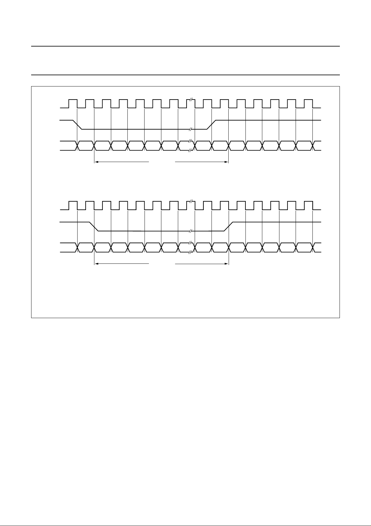
Philips Semiconductors Product specification
Digital TV sound demodulator/decoder TDA9874A
handbook, full pagewidth
SCK
WS
SDO
handbook, full pagewidth
SCK
WS
SDO
LSB MSB LSB MSB
MGK758
one sample
a. I2S-bus format.
LSB MSB LSB MSB
MGK759
one sample
b. MSB-aligned format.
Fig.8 Serial audio interface formats.
2000 Aug 04 50
Page 51

Philips Semiconductors Product specification
Digital TV sound demodulator/decoder TDA9874A
9 LIMITING VALUES
In accordance with the Absolute Maximum Rating System (IEC 60134).
SYMBOL PARAMETER CONDITIONS MIN. MAX. UNIT
V
DDx
∆V
DDx
I
IK
I
OK
I
o
I
DDD
, I
I
DDA
I
lu(prot)
P/out power dissipation per output − 100 mW
P
tot
T
stg
T
amb
V
es
DC supply voltage −0.5 +6.5 V
voltage differences between two V
DC input clamp diode current Vi< −0.5 V or
pins − 550 mV
DDx
−±10 mA
Vi>VDD+ 0.5 V
DC output clamp diode current output type 4 mA Vo< −0.5 V or
−±20 mA
Vo>VDD+ 0.5 V
DC output source or sink current; output type 4 mA −0.5V<VO<VDD+ 0.5 V −±20 mA
, I
SSD
SSA
DC V
DC V
DDD
DDA
or V
or V
current per digital supply pin −±96 mA
SSD
current per analog supply pin −±50 mA
SSA
latch-up protection current 100 − mA
total power dissipation − 0.75 W
storage temperature −55 +125 °C
ambient temperature −20 +70 °C
electrostatic handling voltage note 1 2000 − V
note 2 200 − V
Notes
1. Human body model: C = 100 pF and R = 1.5 kΩ.
2. Machine model: C = 200 pF, L = 0.75 µH and R = 0 Ω.
10 THERMAL CHARACTERISTICS
SYMBOL PARAMETER CONDITIONS VALUE UNIT
R
th(j-a)
thermal resistance from junction to ambient in free air 70 K/W
2000 Aug 04 51
Page 52

Philips Semiconductors Product specification
Digital TV sound demodulator/decoder TDA9874A
11 CHARACTERISTICS
VDD=5V; T
parameters in accordance with system A2; NICAM in accordance with
1kΩmeasurement source resistance for AF inputs; V
level and gain settings according to note 1 with external components of Fig.9; unless otherwise specified.
SYMBOL PARAMETER CONDITIONS MIN. TYP. MAX. UNIT
Digital supplies
V
DDD1
V
SSD1
I
DDD1
V
SSD2
V
DDD3
V
SSD3
I
DDD3
Power failure register
V
pfr
Demodulator supplies and references
V
DDA3
V
SSA3
I
DDA3
V
DEC1
V
SSA2
V
ref1
I
ref1(sink)
Audio supplies and references
V
DDA1
V
SSA1
I
DDA1
V
SSA4
V
ref2
=25°C; settings in accordance with B/G standard; FM deviation ±50 kHz; f
amb
“EBU NICAM 728 specification”
= 300 mV (p-p); bit AGCOFF = 0; bit AGCSLOW = 1;
SIF
= 1 kHz; FM sound
mod
;
digital supply voltage 1 4.5 5.0 5.5 V
digital ground supply 1 − 0.0 − V
digital supply current 1 V
=5.5V 4059 74mA
DDD1
=5.0V 4259 75mA
V
DDD1
digital ground supply 2 − 0.0 − V
digital supply voltage 3 4.5 5.0 5.5 V
digital ground supply 3 − 0.0 − V
digital supply current 3 V
= 5.5 V; SYSCLK off 9 17 21 mA
DDD3
V
= 5.0 V; SYSCLK off 8 16 20 mA
DDD3
power failure response voltage − 4.0 − V
analog supply voltage 3 for
4.5 5.0 5.5 V
demodulator part
analog ground supply 3 for
− 0.0 − V
demodulator part
analog supply current 3 for
demodulator part
analog supply decoupling
V
=5.5V 2432 40mA
DDA3
V
=5.0V 2432 40mA
DDA3
− 3.3 − V
voltage for front-end
analog ground supply 2 − 0.0 − V
analog reference voltage for
− 2 − V
demodulator part
sink current at pin V
ref1
analog supply voltage 1 for
− 200 −µA
4.5 5.0 5.5 V
operational amplifiers
analog ground supply 1 for
− 0.0 − V
operational amplifiers
analog supply current 1 for
operational amplifiers
analog ground supply 4 for
V
= 5.5 V 3 6 10 mA
DDA1
V
= 5.0 V 3 5 10 mA
DDA1
− 0.0 − V
audio DAC part
reference voltage 2 for audio
DACs and operational amplifiers
referenced to V
V
SSA1
DDA1
and
− 50 − %
2000 Aug 04 52
Page 53

Philips Semiconductors Product specification
Digital TV sound demodulator/decoder TDA9874A
SYMBOL PARAMETER CONDITIONS MIN. TYP. MAX. UNIT
Z
(Vref2-VDDA3)
Z
(Vref2-VSSA3)
Digital inputs and outputs
INPUTS
CMOS level input, high drive, pull-down (pins TEST1, TEST2, TP1 and TP2)
V
IL
V
IH
C
i
Z
i
CMOS level input, hysteresis, high drive, pull-up (pin CRESET)
V
IL
V
IH
V
hys
C
i
Z
i
INPUTS/OUTPUTS
impedance between pins V
and V
DDA3
impedance between pins V
and V
SSA3
ref2
ref2
LOW-level input voltage −− 0.3V
HIGH-level input voltage 0.7V
− 20 − kΩ
− 20 − kΩ
V
DDD
−−V
DDD
input capacitance −− 10 pF
input impedance − 50 − kΩ
LOW-level input voltage −− 0.3V
HIGH-level input voltage 0.7V
−−V
DDD
DDD
V
hysteresis voltage − 1.3 − V
input capacitance −− 10 pF
input impedance − 50 − kΩ
I2C-bus level input with Schmitt trigger, open-drain output stage (pins SCL and SDA)
V
IL
V
IH
V
hys
I
LI
C
i
V
OL
C
L
LOW-level input voltage −− 0.3V
HIGH-level input voltage 0.7V
hysteresis voltage − 0.05V
−−V
DDD
− V
DDD
DDD
V
input leakage current −− ±10 µA
input capacitance −− 10 pF
LOW-level output voltage −− 0.6 V
load capacitance −− 400 pF
TTL/CMOS level, high drive, 4 mA 3-state output stage, pull-up (pins PCLK, NICAM, ADDR1, ADDR2, P1, P2, SCK,
WS and SDO)
V
IL
V
IH
C
i
V
OL
V
OH
C
L
Z
i
LOW-level input voltage −− 0.8 V
HIGH-level input voltage 2.0 −−V
input capacitance −− 10 pF
LOW-level output voltage IOL=3mA −− 0.4 V
HIGH-level output voltage IOH= −3 mA 2.4 −−V
load capacitance active pull-up −− 100 pF
input impedance − 50 − kΩ
OUTPUTS
4 mA 3-state output stage (pin SYSCLK)
V
OL
V
OH
LOW-level output voltage IOL=2mA −− 0.3V
HIGH-level output voltage IOH= −2 mA 0.7V
−−V
DDD
DDD
V
2000 Aug 04 53
Page 54

Philips Semiconductors Product specification
Digital TV sound demodulator/decoder TDA9874A
SYMBOL PARAMETER CONDITIONS MIN. TYP. MAX. UNIT
C
L
I
LOZ
SIF1 and SIF2 analog inputs
V
SIF(max)(p-p)
V
SIF(min)(p-p)
AGC AGC range − 24 − dB
f
i
R
i
C
i
∆f
FM
∆f
FM(FS)
∆f
FM(max)
C/N
FM
C/N
N
α
ct
Demodulator performance
V
o(nom)(rms)
THD + N total harmonic distortion plus
load capacitance −− 100 pF
3-state leakage current Vi= 0 to V
maximum composite SIF input
voltage before clipping
(peak-to-peak value)
SIF input level adjustment
0dB
SIF input level adjustment
DDD
−− ±10 µA
− 941 − mV
− 2976 − mV
−10 dB
minimum composite SIF input
voltage for lower limit of AGC
(peak-to-peak value)
SIF input level adjustment
0dB
SIF input level adjustment
− 59 − mV
− 188 − mV
−10 dB
input frequency 4 − 9.2 MHz
input resistance AGCLEV = 0 10 −−kΩ
input capacitance − 7.5 11 pF
FM deviation B/G standard; THD < 1% ±100 −−kHz
FM deviation full-scale level terrestrial FM; level
±150 −−kHz
adjustment 0 dB;
demodulatorfilterbandwidth
set to narrow
maximum FM deviation in high
deviation mode
B/G standard; THD < 1%;
demodulatorfilterbandwidth
±335 −−kHz
set to extra wide
FM carrier-to-noise ratio NFM bandwidth = 6 MHz;
white noise for S/N = 40 dB;
“CCIR468-2”
; quasi peak
NICAM carrier-to-noise ratio NN bandwidth = 6 MHz;
bit error rate = 10−3;
− 77 −
− 66 −
dB
------ Hz
dB
------ Hz
white noise
crosstalk attenuation
fi= 4 to 9.2 MHz 50 −−dB
SIF1 to SIF2
nominal level output voltage
note 1 400 500 600 mV
(RMS value)
noise
from FM source to any
output;f
= 1 kHz;bandwidth
i
− 0.3 0.5 %
20 Hz to 20 kHz;
Vo= 1 V (RMS)
from NICAM source to any
output;f
= 1 kHz;bandwidth
i
− 0.1 0.3 %
20 Hz to 20 kHz;
Vo= 1 V (RMS)
2000 Aug 04 54
Page 55

Philips Semiconductors Product specification
Digital TV sound demodulator/decoder TDA9874A
SYMBOL PARAMETER CONDITIONS MIN. TYP. MAX. UNIT
S/N signal-to-noise ratio SC1 from FM source to any
output; Vo= 1 V (RMS);
“CCIR468-2”
; quasi peak
SC2 from FM source to any
output; V
“CCIR468-2”
= 1 V (RMS);
o
; quasi peak
SC1 during use of high
deviation mode from
FM source to any output;
= 1 V (RMS);
V
o
“CCIR468-2”
; quasi peak
NICAM source;
V
= 1 V (RMS);
o
B
−3dB
“CCIR468-2”
−3 dB bandwidth from FM source to any
; quasi peak
output
from NICAM source to any
output
f
res
α
cs(dual)
α
cs(stereo)
α
AM
frequency response
20 Hz to 14 kHz
from FM/NICAM to any
output; reference 1 kHz
dual signal channel separation note 3 65 70 − dB
stereo channel separation note 4 40 45 − dB
AM suppression for FM AM:1 kHz, 30% modulation;
reference:fi= 1 kHz;50 kHz
deviation
dm
AM
AM demodulation SIF level 100 mV (RMS);
54% AM; 1 kHz AF;
“CCIR468-2”
; quasi peak
IDENTIFICATION FOR FM SYSTEMS
mod
C/N
p
p
pilot modulation for identification 25 50 75 %
pilot sideband carrier-to-noise
ratio for identification start
hys
(tun)
f
ident
hysteresis −− 2dB
identification window B/G stereo
slow mode 116.85 − 118.12 Hz
medium mode 116.11 − 118.89 Hz
fast mode 114.65 − 120.46 Hz
B/G dual
slow mode 273.44 − 274.81 Hz
medium mode 272.07 − 276.20 Hz
fast mode 270.73 − 277.60 Hz
t
ident(on)
total identification time on slow mode −− 2s
medium mode −− 1s
fast mode −− 0.5 s
64 70 − dB
60 66 − dB
62 68 − dB
NICAM in accordance with
“EBU specification”
; note 2
14.5 15 − kHz
14.5 15 − kHz
−2 − +1 dB
50 −−dB
36 45 − dB
− 27 −
dB
------ Hz
2000 Aug 04 55
Page 56

Philips Semiconductors Product specification
Digital TV sound demodulator/decoder TDA9874A
SYMBOL PARAMETER CONDITIONS MIN. TYP. MAX. UNIT
t
ident(off)
Mono and external inputs
V
i(nom)(rms)
V
i(clip)(rms)
R
i
Analog audio outputs
V
o(clip)(rms)
R
o
R
L(AC)
R
L(DC)
C
L
V
offset(DC)
α
mute
B
line
G
ro
PSRR power supply ripple rejection f
Audio performance
THD + N total harmonic distortion plus
S/N signal-to-noise ratio reference voltage
α
ct
α
cs
total identification time off slow mode −− 2s
medium mode −− 1s
fast mode −− 0.5 s
nominal level input voltage
note 1 − 500 − mV
(RMS value)
clipping level input voltage
THD < 3%; note 5 1250 1400 − mV
(RMS value)
input resistance note 5 28 35 42 kΩ
clipping level output voltage
THD < 3% 1400 −−mV
(RMS value)
output resistance 150 250 375 Ω
AC load resistor 10 −−kΩ
DC load resistor 10 −−kΩ
output load capacitor − 10 12 nF
static DC offset voltage − 30 70 mV
mute suppression nominal input signal from
80 −−dB
any source; fi= 1 kHz;
note 1
bandwidth from external and mono
20 −−kHz
source; −3 dB bandwidth
roll-off gain at 14.5 kHz from any source −3 −2 − dB
= 70 Hz;
ripple
V
= 100 mV (peak);
ripple
C
=47µF; signal from
Vref
40 45 − dB
I2S-bus
noise
V
fi= 1 kHz; bandwidth
i=Vo
= 1 V (RMS);
− 0.1 0.3 %
20 Hz to 20 kHz; from
external or mono input to
output copy
78 90 − dB
= 1.4 V (RMS);
V
o
fi= 1 kHz;
“CCIR468-2”
;
quasi peak; from external or
mono input to output copy
crosstalk attenuation between any analog input
70 −−dB
pairs; fi= 1 kHz
channel separation between left and right of
65 −−dB
external input pair
between left and right of
60 −−dB
output pair
2000 Aug 04 56
Page 57

Philips Semiconductors Product specification
Digital TV sound demodulator/decoder TDA9874A
SYMBOL PARAMETER CONDITIONS MIN. TYP. MAX. UNIT
Crystal specification (fundamental mode)
f
xtal
C
L
C
1
C
0
Φ
pull
R
R
R
N
∆T temperature range −20 +25 +70 °C
X
J
X
D
X
A
crystal frequency note 6 − 24.576 − MHz
load capacitance − 20 − pF
series capacitance − 20 − fF
parallel capacitance −− 7pF
pulling sensitivity CL changed from
18 to 16 pF
− 25 −
10
-----------
pF
6–
equivalent series resistance at nominal frequency −− 30 Ω
equivalent series resistance of
2R
R
−−Ω
unwanted mode
adjustment tolerance −− ±30 10
drift across temperature range −− ±30 10
ageing −− ±5
−6
−6
10
----------year
6–
Notes
1. Definition of levels and level setting:
a) The full-scale level for analog audio signals is 1.4 V (RMS).
b) The nominal level at the digital crossbar switch is defined at −15 dB (full-scale).
c) Nominal audio input levels: external, mono: 500 mV (RMS); −9 dB (full-scale).
2. Audio performance is limited by the dynamic range of the NICAM 728 system. Due to companding, the quantization
noise is never lower than −62 dB with respect to the input level.
3. FM source; in dual mode only A (respectively B) signal modulated; measured at B (respectively A) channel output;
Vo= 1 V (RMS) of modulated channel.
4. FM source; in stereo mode only L (respectively R) signal modulated; measured at R (respectively L) channel output;
Vo= 1 V (RMS) of modulated channel.
5. If the supply voltage for the TDA9874A is switched off, because of the ESD protection circuitry, all audio input pins
are short-circuited.
6. The Philips crystal (order number 9922 520 20106) is suitable for this application.
2000 Aug 04 57
Page 58

This text is here in white to force landscape pages to be rotated correctly when browsing through the pdf in the Acrobat reader.This text is here in
_white to force landscape pages to be rotated correctly when browsing through the pdf in the Acrobat reader.This text is here inThis text is here in
white to force landscape pages to be rotated correctly when browsing through the pdf in the Acrobat reader. white to force landscape pages to be ...
2000 Aug 04 58
Table 90 Level setting FM, AM and NICAM at 0 dB (full-scale) = 1.4 V (RMS)
LEVEL
ADJUSTMENT
SETTING
NOMINAL LEVEL
AT CROSSBAR
(spread of ±0.5 dB
due to different
transmitter
references)
DAC GAIN
SETTING
NOMINAL OUTPUT
VOLTAGE V
+6 dB 500 mV (RMS)
SOURCE
FM
M standard
FM
B/G, D/K, I
standard
AM
TRANSMITTERNOMINAL
MODULATION DEPTH
NOMINAL LEVEL AT
DEMODULATOR OUTPUT
15 kHz deviation −24dB (full-scale) +9 dB −15 dB (full-scale)
27 kHz deviation −19dB (full-scale) +4 dB
54% −19 dB (full-scale) +4 dB
L/L accent
standard
NICAM
−11.2 dB (full-scale) −18 dB (full-scale) +3 dB
B/G, D/K,
L standard
NICAM
−15.8 dB (full-scale) −23 dB (full-scale) +8 dB
I standard
Table 91 Level setting SAT FM at 0 dB (full-scale) = 1.4 V (RMS)
Philips Semiconductors Product specification
Digital TV sound demodulator/decoder TDA9874A
O
SOURCE
SAT FM
stereo
SAT FM
mono
TRANSMITTER
MAXIMUM MODULATION
DEPTH
NOMINAL LEVEL AT
DEMODULATOR OUTPUT
LEVEL
ADJUSTMENT
SETTING
MAXIMUM LEVEL
AT CROSSBAR
DAC GAIN
SETTING
MAXIMUMOUTPUT
VOLTAGE V
50 kHz deviation −13dB (full-scale) +4 dB −9 dB (full-scale) +6 dB 1 V (RMS)
85 kHz deviation −9dB (full-scale) 0 dB
O
Page 59
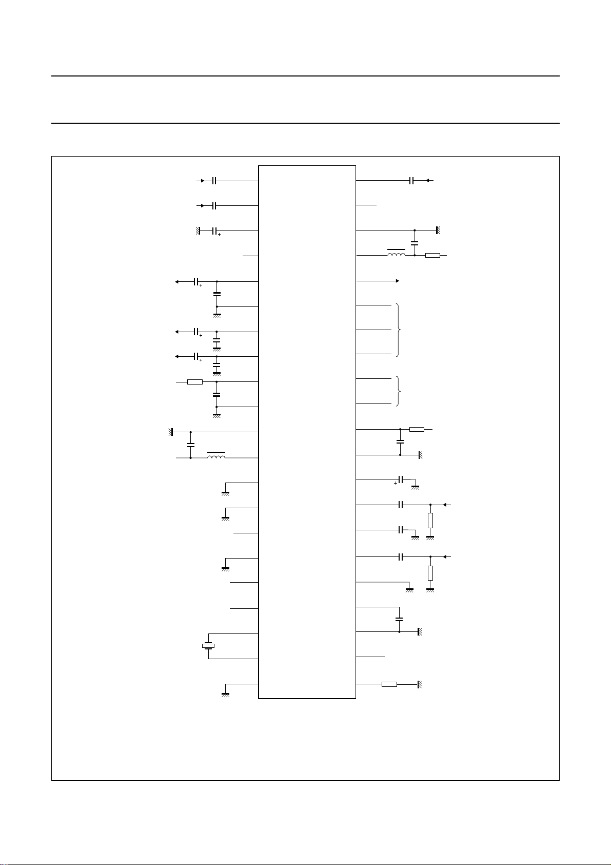
Philips Semiconductors Product specification
Digital TV sound demodulator/decoder TDA9874A
12 APPLICATION DIAGRAMS
handbook, full pagewidth
5 V
5 V
2.2 µF
2.2 µF
2.2 µF
10 Ω
24.576
MHz
470
nF
470 nF
470 nF
47 µF
(2)
Lx
(1)
(1)
10
nF
10
nF
10
nF
470
nF
EXTIR
EXTIL
V
ref2
OUTM
V
SSA4
OUTL
OUTR
V
DDA1
V
SSA1
V
SSD1
V
DDD1
V
SSD2
TP2
NICAM
TP1
PCLK
ADDR1
XTALO
XTALI
1
2
3
P2
4
5
6
7
8
9
10
TDA9874APS
11
12
13
14
15
16
17
18
19
20
42
41
40
39
38
37
36
35
34
33
32
31
30
29
28
27
26
25
24
23
MONOIN
P1
V
SSD3
V
DDD3
SYSCLK
SCK
WS
SDO
SDA
SCL
V
DDA3
V
SSA3
CRESET
SIF1
V
ref1
SIF2
TEST1
V
DEC
V
SSA2
ADDR2
(2)
Lx
1 µF
47 pF
100 nF
47 pF
470 nF
470 nF
2
I
S-bus
2
I
C-bus
10 Ω
470 nF
(1)
decoupling
capacitor
470 nF
3.3 Ω
5 V
5 V
50 Ω
50 Ω
I
TEST2
(1)
21
22
MHB591
8.2 kΩ
ref
All analog and digital supply ground pins are connected internally and should be connected via a massive external ground plate.
(1) TP1, TP2, TEST1 and TEST2 should be connected to V
during normal operation.
SSD
(2) Lx: ferrite bead, e.g. Murata type BLM 31A601S.
Fig.9 Application diagram (SDIP42 version).
2000 Aug 04 59
Page 60
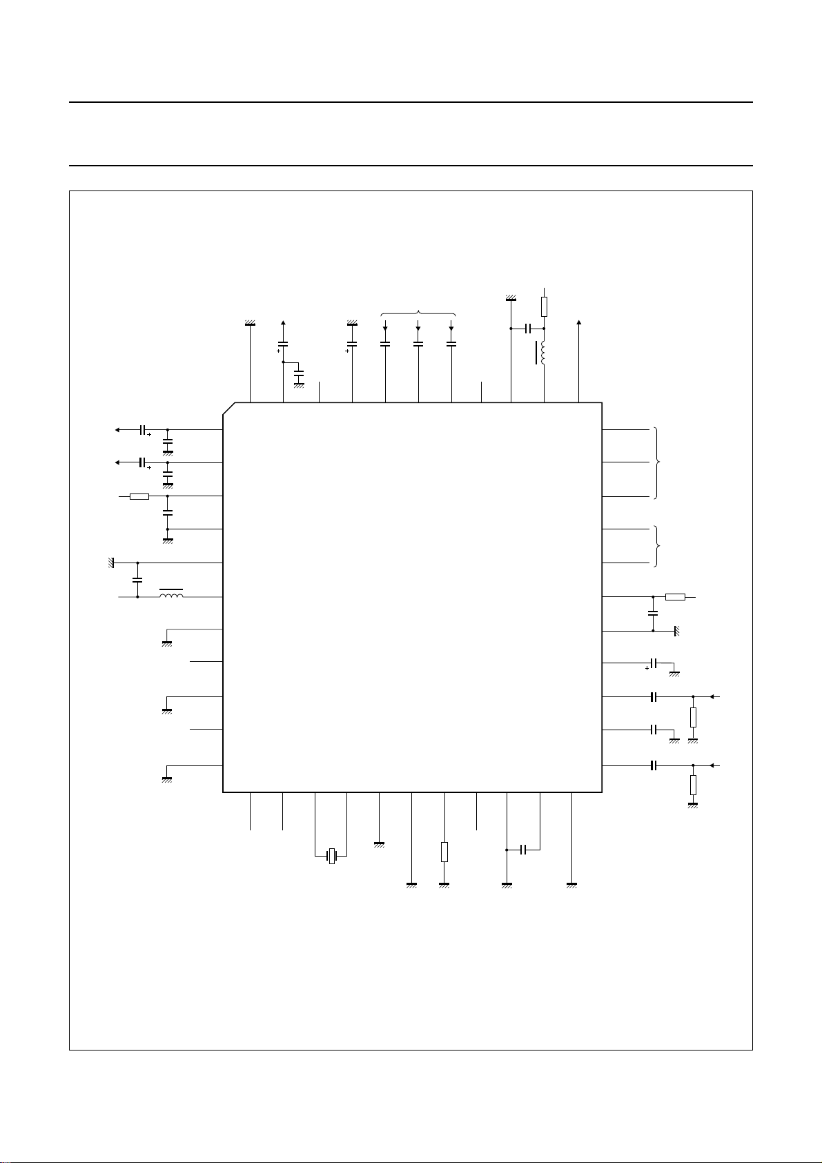
Philips Semiconductors Product specification
Digital TV sound demodulator/decoder TDA9874A
handbook, full pagewidth
2.2 µF
2.2 µF
10 Ω
5 V
470
5 V
nF
5 V
external input
47
2.2 µF
SSA4
OUTM
V
OUTL
10
nF
OUTR
10
nF
V
DDA1
470
nF
V
SSA1
V
SSD1
V
DDD1
(2)
Lx
V
SSD2
n.c.
(1)
(1)
TP2
NICAM
TP1
44 43 42 41 40 39 38 37 36 35 34
1
2
3
4
5
6
7
8
9
10
11
12 13 14 15 16 17 18 19 20 21 22
PCLK
ADDR1
P2
XTALO
24.576
MHz
ref2
V
XTALI
470nF470nF470
µF
EXTIL
TDA9874AH
TP3
(1)
EXTIR
TEST2
(1)
MONOIN
ref
I
8.2 kΩ
nF
P1
ADDR2
SSD3VDDD3
V
SSA2
V
470
nF
DEC
V
470 nF
decoupling
capacitor
3.3 Ω
Lx
(2)
SYSCLK
TEST1
(1)
33
32
31
30
29
28
27
26
25
24
23
SCK
WS
SDO
SDA
SCL
V
V
CRESET
SIF1
V
SIF2
MHB592
DDA3
SSA3
ref1
1 µF
47 pF
100 nF
47 pF
2
S-bus
I
2
C-bus
I
10 Ω
470 nF
5 V
50 Ω
50 Ω
All analog and digital supply ground pins are connected internally and should be connected via a massive external ground plate.
(1) TP1, TP2, TP3, TEST1 and TEST2 should be connected to V
during normal operation.
SSD
(2) Lx: ferrite bead, e.g. Murata type BLM 31A601S.
Fig.10 Application diagram (QFP44 version).
2000 Aug 04 60
Page 61
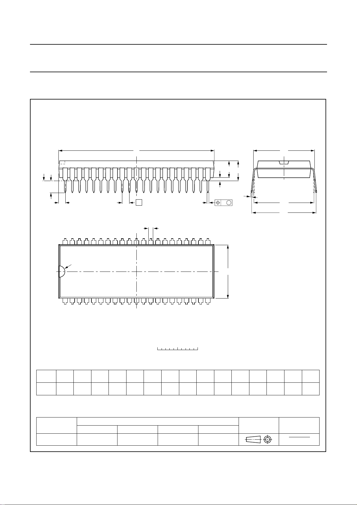
Philips Semiconductors Product specification
Digital TV sound demodulator/decoder TDA9874A
13 PACKAGE OUTLINES
SDIP42: plastic shrink dual in-line package; 42 leads (600 mil)
SOT270-1
seating plane
L
Z
42
1
pin 1 index
D
A
2
A
A
1
e
b
w M
b
1
22
E
21
c
M
(e )
M
E
1
H
0 5 10 mm
scale
DIMENSIONS (mm are the original dimensions)
A
A
A
UNIT b
Note
1. Plastic or metal protrusions of 0.25 mm maximum per side are not included.
max.
mm
5.08 0.51 4.0
OUTLINE
VERSION
SOT270-1 MS-020
12
min.
max.
IEC JEDEC EIAJ
1.3
0.8
b
1
0.53
0.40
REFERENCES
0.32
0.23
cEe M
(1) (1)
D
38.9
38.4
2000 Aug 04 61
14.0
13.7
1
L
M
E
3.2
15.80
2.9
15.24
EUROPEAN
PROJECTION
17.15
15.90
e
w
H
0.181.778 15.24
ISSUE DATE
95-02-04
99-12-27
max.
1.73
(1)
Z
Page 62
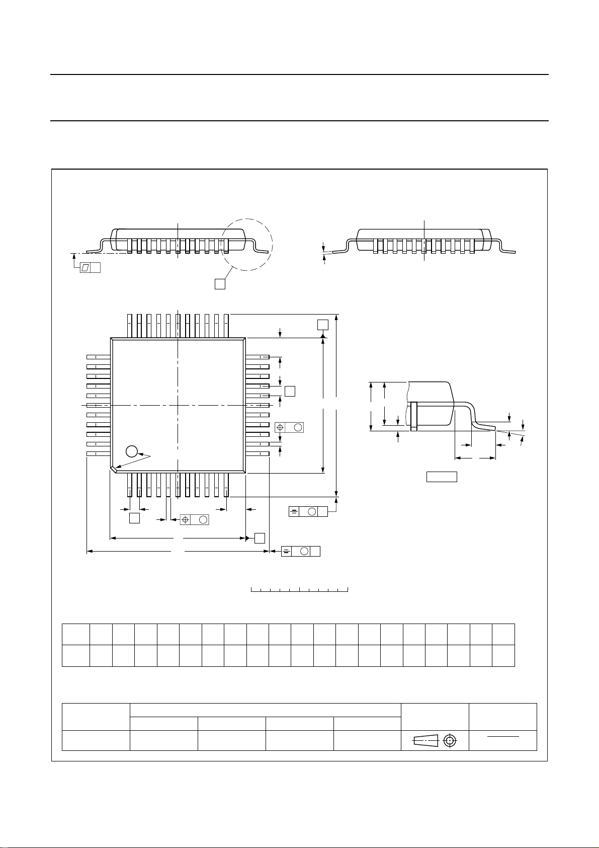
Philips Semiconductors Product specification
Digital TV sound demodulator/decoder TDA9874A
QFP44: plastic quad flat package; 44 leads (lead length 2.35 mm); body 14 x 14 x 2.2 mm
c
y
X
33 23
34
pin 1 index
44
1
Z
22
E
e
w M
b
p
12
11
A
H
E
E
A
2
A
A
1
detail X
L
L
p
SOT205-1
(A )
3
θ
Z
e
w M
b
p
D
H
D
D
B
v M
0 5 10 mm
scale
DIMENSIONS (mm are the original dimensions)
mm
A
max.
2.60
0.25
0.05
2.3
2.1
0.25
0.50
0.35
0.25
0.14
UNIT A1A2A3bpcE
(1)
(1) (1)(1)
D
14.1
13.9
eH
H
14.1
13.9
19.2
1
18.2
Note
1. Plastic or metal protrusions of 0.25 mm maximum per side are not included.
OUTLINE
VERSION
SOT205-1
IEC JEDEC EIAJ
133E01
REFERENCES
2000 Aug 04 62
v M
D
A
B
E
19.2
18.2
LL
p
2.0
1.2
0.152.35 0.10.3
EUROPEAN
PROJECTION
Z
D
2.4
1.8
Zywv θ
E
o
2.4
7
o
1.8
0
ISSUE DATE
97-08-01
99-12-27
Page 63

Philips Semiconductors Product specification
Digital TV sound demodulator/decoder TDA9874A
14 SOLDERING
14.1 Introduction
Thistextgivesaverybriefinsighttoa complex technology.
A more in-depth account of soldering ICs can be found in
our
“Data Handbook IC26; Integrated Circuit Packages”
(document order number 9398 652 90011).
There is no soldering method that is ideal for all IC
packages. Wave soldering is often preferred when
through-holeandsurfacemountcomponents are mixedon
one printed-circuit board. However, wave soldering is not
always suitable for surface mount ICs, or for printed-circuit
boards with high population densities. In these situations
reflow soldering is often used.
14.2 Through-hole mount packages
14.2.1 SOLDERING BY DIPPING OR BY SOLDER WAVE
The maximum permissible temperature of the solder is
260 °C; solder at this temperature must not be in contact
with the joints for more than 5 seconds. The total contact
time of successive solder waves must not exceed
5 seconds.
The device may be mounted up to the seating plane, but
the temperature of the plastic body must not exceed the
specified maximum storage temperature (T
printed-circuit board has been pre-heated, forced cooling
may be necessary immediately after soldering to keep the
temperature within the permissible limit.
14.2.2 MANUAL SOLDERING
Apply the soldering iron (24 V or less) to the lead(s) of the
package, either below the seating plane or not more than
2 mm above it. If the temperature of the soldering iron bit
is less than 300 °C it may remain in contact for up to
10 seconds. If the bit temperature is between
300 and 400 °C, contact may be up to 5 seconds.
14.3 Surface mount packages
14.3.1 REFLOW SOLDERING
Reflow soldering requires solder paste (a suspension of
fine solder particles, flux and binding agent) to be applied
totheprinted-circuitboardbyscreenprinting,stencillingor
pressure-syringe dispensing before package placement.
Several methods exist for reflowing; for example,
infrared/convection heating in a conveyor type oven.
Throughput times (preheating, soldering and cooling) vary
between 100 and 200 seconds depending on heating
method.
stg(max)
). If the
Typical reflow peak temperatures range from
215 to 250 °C. The top-surface temperature of the
packages should preferable be kept below 230 °C.
14.3.2 WAVE SOLDERING
Conventional single wave soldering is not recommended
forsurfacemountdevices(SMDs)orprinted-circuit boards
with a high component density, as solder bridging and
non-wetting can present major problems.
To overcome these problems the double-wave soldering
method was specifically developed.
If wave soldering is used the following conditions must be
observed for optimal results:
• Use a double-wave soldering method comprising a
turbulent wave with high upward pressure followed by a
smooth laminar wave.
• For packages with leads on two sides and a pitch (e):
– larger than or equal to 1.27 mm, the footprint
longitudinal axis is preferred to be parallel to the
transport direction of the printed-circuit board;
– smaller than 1.27 mm, the footprint longitudinal axis
must be parallel to the transport direction of the
printed-circuit board.
The footprint must incorporate solder thieves at the
downstream end.
• Forpackageswithleadsonfoursides, the footprint must
be placed at a 45° angle to the transport direction of the
printed-circuit board. The footprint must incorporate
solder thieves downstream and at the side corners.
During placement and before soldering, the package must
be fixed with a droplet of adhesive. The adhesive can be
applied by screen printing, pin transfer or syringe
dispensing. The package can be soldered after the
adhesive is cured.
Typical dwell time is 4 seconds at 250 °C.
A mildly-activated flux will eliminate the need for removal
of corrosive residues in most applications.
14.3.3 MANUAL SOLDERING
Fix the component by first soldering two
diagonally-opposite end leads. Use a low voltage (24 V or
less) soldering iron applied to the flat part of the lead.
Contact time must be limited to 10 seconds at up to
300 °C.
When using a dedicated tool, all other leads can be
soldered in one operation within 2 to 5 seconds between
270 and 320 °C.
2000 Aug 04 63
Page 64

Philips Semiconductors Product specification
Digital TV sound demodulator/decoder TDA9874A
14.4 Suitability of IC packages for wave, reflow and dipping soldering methods
MOUNTING PACKAGE
Through-hole mount DBS, DIP, HDIP, SDIP, SIL suitable
WAVE REFLOW
(2)
− suitable
(1)
DIPPING
Surface mount BGA, SQFP not suitable suitable −
SOLDERING METHOD
HLQFP, HSQFP, HSOP, HTSSOP, SMS not suitable
(4)
PLCC
, SO, SOJ suitable suitable −
LQFP, QFP, TQFP not recommended
SSOP, TSSOP, VSO not recommended
(3)
(4)(5)
(6)
suitable −
suitable −
suitable −
Notes
1. All surface mount (SMD) packages are moisture sensitive. Depending upon the moisture content, the maximum
temperature (with respect to time) and body size of the package, there is a risk that internal or external package
cracks may occur due to vaporization of the moisture in them (the so called popcorn effect). For details, refer to the
Drypack information in the
“Data Handbook IC26; Integrated Circuit Packages; Section: Packing Methods”
.
2. For SDIP packages, the longitudinal axis must be parallel to the transport direction of the printed-circuit board.
3. These packages are not suitable for wave soldering as a solder joint between the printed-circuit board and heatsink
(at bottom version) can not be achieved, and as solder may stick to the heatsink (on top version).
4. If wave soldering is considered, then the package must be placed at a 45° angle to the solder wave direction.
The package footprint must incorporate solder thieves downstream and at the side corners.
5. Wave soldering is only suitable for LQFP, QFP and TQFP packages with a pitch (e) equal to or larger than 0.8 mm;
it is definitely not suitable for packages with a pitch (e) equal to or smaller than 0.65 mm.
6. Wave soldering is only suitable for SSOP and TSSOP packages with a pitch (e) equal to or larger than 0.65 mm; it is
definitely not suitable for packages with a pitch (e) equal to or smaller than 0.5 mm.
2000 Aug 04 64
Page 65

Philips Semiconductors Product specification
Digital TV sound demodulator/decoder TDA9874A
15 DATA SHEET STATUS
DATA SHEET STATUS
PRODUCT
STATUS
DEFINITIONS
(1)
Objective specification Development This data sheet contains the design target or goal specifications for
product development. Specification may change in any manner without
notice.
Preliminary specification Qualification This data sheet contains preliminary data, and supplementary data will be
published at a later date. Philips Semiconductors reserves the right to
make changes at any time without notice in order to improve design and
supply the best possible product.
Product specification Production This data sheet contains final specifications. Philips Semiconductors
reserves the right to make changes at any time without notice in order to
improve design and supply the best possible product.
Note
1. Please consult the most recently issued data sheet before initiating or completing a design.
16 DEFINITIONS
Short-form specification The data in a short-form
specification is extracted from a full data sheet with the
same type number and title. For detailed information see
the relevant data sheet or data handbook.
Limiting values definition Limiting values given are in
accordance with the Absolute Maximum Rating System
(IEC 60134). Stress above one or more of the limiting
values may cause permanent damage to the device.
These are stress ratings only and operation of the device
attheseoratanyotherconditionsabovethosegivenin the
Characteristics sections of the specification is not implied.
Exposure to limiting values for extended periods may
affect device reliability.
Application information Applications that are
described herein for any of these products are for
illustrative purposes only. Philips Semiconductors make
norepresentationorwarrantythatsuch applications will be
suitable for the specified use without further testing or
modification.
17 DISCLAIMERS Life support applications These products are not
designed for use in life support appliances, devices, or
systems where malfunction of these products can
reasonably be expected to result in personal injury. Philips
Semiconductorscustomersusingorselling these products
for use in such applications do so at their own risk and
agree to fully indemnify Philips Semiconductors for any
damages resulting from such application.
Right to make changes Philips Semiconductors
reserves the right to make changes, without notice, in the
products, including circuits, standard cells, and/or
software, described or contained herein in order to
improve design and/or performance. Philips
Semiconductors assumes no responsibility or liability for
theuseofanyoftheseproducts, conveys no licence or title
under any patent, copyright, or mask work right to these
products,andmakesnorepresentationsorwarrantiesthat
these products are free from patent, copyright, or mask
work right infringement, unless otherwise specified.
2
18 PURCHASE OF PHILIPS I
Purchase of Philips I
C COMPONENTS
2
C components conveys a license under the Philips’ I2C patent to use the
components in the I2C system provided the system conforms to the I2C specification defined by
Philips. This specification can be ordered using the code 9398 393 40011.
2000 Aug 04 65
Page 66

Philips Semiconductors Product specification
Digital TV sound demodulator/decoder TDA9874A
NOTES
2000 Aug 04 66
Page 67

Philips Semiconductors Product specification
Digital TV sound demodulator/decoder TDA9874A
NOTES
2000 Aug 04 67
Page 68

Philips Semiconductors – a w orldwide compan y
Argentina: see South America
Australia: 3 Figtree Drive, HOMEBUSH, NSW 2140,
Tel. +61 2 9704 8141, Fax. +61 2 9704 8139
Austria: Computerstr. 6, A-1101 WIEN, P.O. Box 213,
Tel. +43 1 60 101 1248, Fax. +43 1 60 101 1210
Belarus: Hotel Minsk Business Center, Bld. 3, r. 1211, Volodarski Str. 6,
220050 MINSK, Tel. +375 172 20 0733, Fax. +375 172 20 0773
Belgium: see The Netherlands
Brazil: see South America
Bulgaria: Philips Bulgaria Ltd., Energoproject, 15th floor,
51 James Bourchier Blvd., 1407 SOFIA,
Tel. +359 2 68 9211, Fax. +359 2 68 9102
Canada: PHILIPS SEMICONDUCTORS/COMPONENTS,
Tel. +1 800 234 7381, Fax. +1 800 943 0087
China/Hong Kong: 501 Hong Kong Industrial Technology Centre,
72 Tat Chee Avenue, Kowloon Tong, HONG KONG,
Tel. +852 2319 7888, Fax. +852 2319 7700
Colombia: see South America
Czech Republic: see Austria
Denmark: Sydhavnsgade 23, 1780 COPENHAGEN V,
Tel. +45 33 29 3333, Fax. +45 33 29 3905
Finland: Sinikalliontie 3, FIN-02630 ESPOO,
Tel. +358 9 615 800, Fax. +358 9 6158 0920
France: 51 Rue Carnot, BP317, 92156 SURESNES Cedex,
Tel. +33 1 4099 6161, Fax. +33 1 4099 6427
Germany: Hammerbrookstraße 69, D-20097 HAMBURG,
Tel. +49 40 2353 60, Fax. +49 40 2353 6300
Hungary: see Austria
India: Philips INDIA Ltd, Band Box Building, 2nd floor,
254-D, Dr. Annie Besant Road, Worli, MUMBAI 400 025,
Tel. +91 22 493 8541, Fax. +91 22 493 0966
Indonesia: PTPhilips DevelopmentCorporation, SemiconductorsDivision,
Gedung Philips, Jl. Buncit Raya Kav.99-100, JAKARTA 12510,
Tel. +62 21 794 0040 ext. 2501, Fax. +62 21 794 0080
Ireland: Newstead, Clonskeagh, DUBLIN 14,
Tel. +353 1 7640 000, Fax. +353 1 7640 200
Israel: RAPAC Electronics, 7 Kehilat Saloniki St, PO Box 18053,
TEL AVIV 61180, Tel. +972 3 645 0444, Fax. +972 3 649 1007
Italy: PHILIPS SEMICONDUCTORS,Via Casati, 23 - 20052 MONZA (MI),
Tel. +39 039 203 6838, Fax +39 039 203 6800
Japan: Philips Bldg 13-37, Kohnan 2-chome, Minato-ku,
TOKYO 108-8507, Tel. +81 3 3740 5130, Fax. +81 3 3740 5057
Korea: Philips House, 260-199 Itaewon-dong, Yongsan-ku, SEOUL,
Tel. +82 2 709 1412, Fax. +82 2 709 1415
Malaysia: No. 76 Jalan Universiti, 46200 PETALING JAYA, SELANGOR,
Tel. +60 3 750 5214, Fax. +60 3 757 4880
Mexico: 5900 Gateway East, Suite 200, EL PASO, TEXAS 79905,
Tel. +9-5 800 234 7381, Fax +9-5 800 943 0087
Middle East: see Italy
Netherlands: Postbus 90050, 5600 PB EINDHOVEN, Bldg. VB,
Tel. +31 40 27 82785, Fax. +31 40 27 88399
New Zealand: 2 Wagener Place, C.P.O. Box 1041, AUCKLAND,
Tel. +64 9 849 4160, Fax. +64 9 849 7811
Norway: Box 1, Manglerud 0612, OSLO,
Tel. +47 22 74 8000, Fax. +47 22 74 8341
Pakistan: see Singapore
Philippines: Philips Semiconductors Philippines Inc.,
106 Valero St. Salcedo Village, P.O. Box 2108 MCC, MAKATI,
Metro MANILA, Tel. +63 2 816 6380, Fax. +63 2 817 3474
Poland: Al.Jerozolimskie 195 B, 02-222 WARSAW,
Tel. +48 22 5710 000, Fax. +48 22 5710 001
Portugal: see Spain
Romania: see Italy
Russia: Philips Russia, Ul. Usatcheva 35A, 119048 MOSCOW,
Tel. +7 095 755 6918, Fax. +7 095 755 6919
Singapore: Lorong 1, Toa Payoh, SINGAPORE 319762,
Tel. +65 350 2538, Fax. +65 251 6500
Slovakia: see Austria
Slovenia: see Italy
South Africa: S.A. PHILIPS Pty Ltd., 195-215 Main Road Martindale,
2092 JOHANNESBURG, P.O. Box 58088 Newville 2114,
Tel. +27 11 471 5401, Fax. +27 11 471 5398
South America: Al. Vicente Pinzon, 173, 6th floor,
04547-130 SÃO PAULO, SP, Brazil,
Tel. +55 11 821 2333, Fax. +55 11 821 2382
Spain: Balmes 22, 08007 BARCELONA,
Tel. +34 93 301 6312, Fax. +34 93 301 4107
Sweden: Kottbygatan 7, Akalla, S-16485 STOCKHOLM,
Tel. +46 8 5985 2000, Fax. +46 8 5985 2745
Switzerland: Allmendstrasse 140, CH-8027 ZÜRICH,
Tel. +41 1 488 2741 Fax. +41 1 488 3263
Taiwan: Philips Semiconductors, 5F, No. 96, Chien Kuo N. Rd., Sec. 1,
TAIPEI, Taiwan Tel. +886 2 2134 2451, Fax. +886 2 2134 2874
Thailand: PHILIPS ELECTRONICS (THAILAND) Ltd.,
60/14 MOO 11, Bangna Trad Road KM. 3, Bagna, BANGKOK 10260,
Tel. +66 2 361 7910, Fax. +66 2 398 3447
Turkey: Yukari Dudullu, Org. San. Blg., 2.Cad. Nr. 28 81260 Umraniye,
ISTANBUL, Tel. +90 216 522 1500, Fax. +90 216 522 1813
Ukraine: PHILIPS UKRAINE, 4 Patrice Lumumba str., Building B, Floor 7,
252042 KIEV, Tel. +380 44 264 2776, Fax. +380 44 268 0461
United Kingdom: Philips Semiconductors Ltd., 276 Bath Road, Hayes,
MIDDLESEX UB3 5BX, Tel. +44 208 730 5000, Fax. +44 208 754 8421
United States: 811 East Arques Avenue, SUNNYVALE, CA 94088-3409,
Tel. +1 800 234 7381, Fax. +1 800 943 0087
Uruguay: see South America
Vietnam: see Singapore
Yugoslavia: PHILIPS, Trg N. Pasica 5/v, 11000 BEOGRAD,
Tel. +381 11 3341 299, Fax.+381 11 3342 553
For all other countries apply to: Philips Semiconductors,
Marketing Communications, Building BE-p, P.O. Box 218, 5600 MD EINDHOVEN,
The Netherlands, Fax. +31 40 27 24825
© Philips Electronics N.V. SCA
All rights are reserved. Reproduction in whole or in part is prohibited without the prior written consent of the copyright owner.
The information presented in this document does not form part of any quotation or contract,isbelievedtobeaccurate and reliable and may be changed
without notice. No liability will be accepted by the publisher for any consequence of its use. Publication thereof does not convey nor imply any license
under patent- or other industrial or intellectual property rights.
2000
Internet: http://www.semiconductors.philips.com
70
Printed in The Netherlands 753504/02/pp68 Date of release: 2000 Aug 04 Document order number: 9397 750 06927
 Loading...