

Page 1
INTEGRATED CIRCUITS
DATA SH EET
TDA9725
Y/C automatic adjustment
processor (VHS standard)
Product specification
Supersedes data of 1995 Dec 06
File under Integrated Circuits, IC02
1996 Oct 14
Page 2
Philips Semiconductors Product specification
Y/C automatic adjustment processor
TDA9725
(VHS standard)
FEATURES
• Automatic adjustment by control loops
• Integrated filters
• Simple SVHS playback
• Colour sequence correction for long-play still mode
• Automatic gain control for FM.
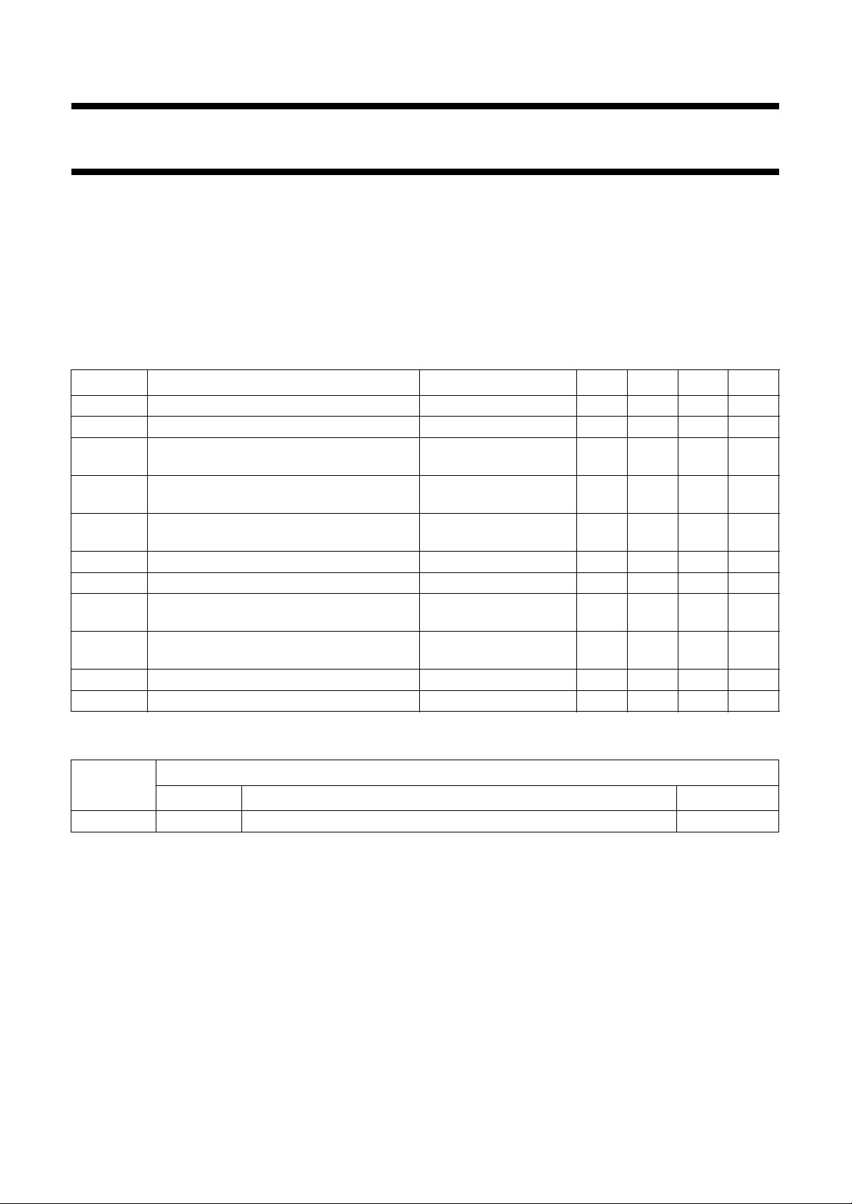
QUICK REFERENCE DATA
SYMBOL PARAMETER CONDITIONS MIN. TYP. MAX. UNIT
V
I
V
CC
CC
i(p-p)
supply voltage 4.5 5.0 5.5 V
supply current VCC= 5 V; playback 140 170 200 mA
video input voltage; CVBS signal
(peak-to-peak value)
V
oREC(p-p)
video output record voltage
(peak-to-peak value)
V
oPB(p-p)
video output playback voltage
(peak-to-peak value)
V
iFM(p-p)
V
oFM(p-p)
V
CFT(p-p)
FM input voltage (peak-to-peak value) FM AGC active 63 200 632 mV
FM output voltage (peak-to-peak value) RL=1kΩ 0.7 0.9 1.1 V
chrominance input voltage (+FM) from tape
(peak-to-peak value)
V
CTT(p-p)
chrominance output voltage to tape
(peak-to-peak value)
T
stg
T
amb
storage temperature −25 − +150 °C
operating ambient temperature −20 − +70 °C
GENERAL DESCRIPTION
The TDA9725 is an integrated circuit for chrominance and
luminance processing (record and playback) in VHS tape
recorders for PAL, SECAM/ME and NTSC systems
(4.43 MHz playback only) with internal filter and without
adjustments.
0.6 1.0 2.0 V
video/sync = 7/3 2.03 2.14 2.25 V
video/sync = 7/3;
2.03 2.14 2.25 V
nominal FM signal
11 110 310 mV
467 660 932 mV
ORDERING INFORMATION
TYPE
NUMBER
NAME DESCRIPTION VERSION
PACKAGE
TDA9725 SDIP52 plastic shrink dual in-line package; 52 leads (600 mil) SOT247-1
1996 Oct 14 2
Page 3
Philips Semiconductors Product specification
Y/C automatic adjustment processor
(VHS standard)
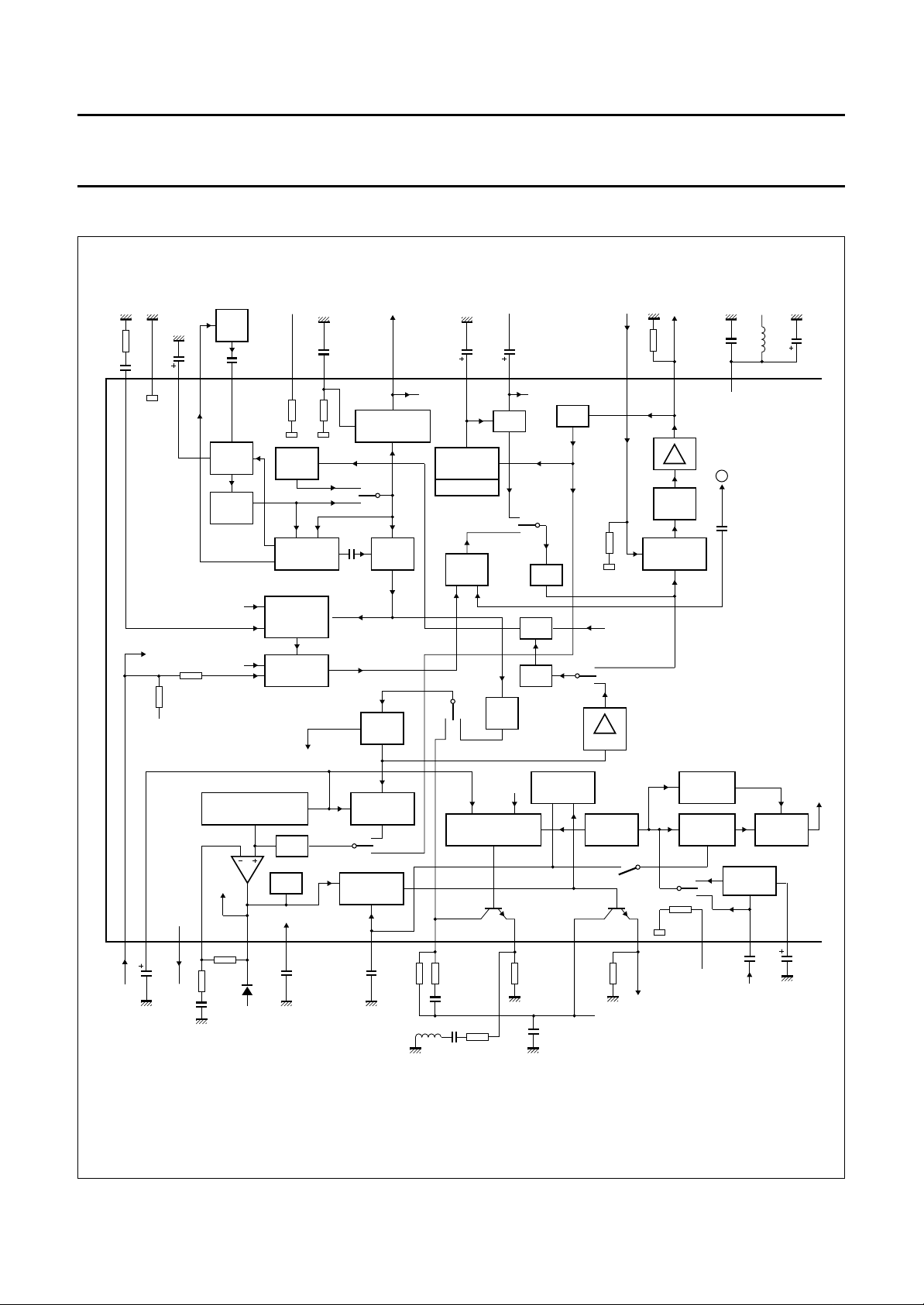
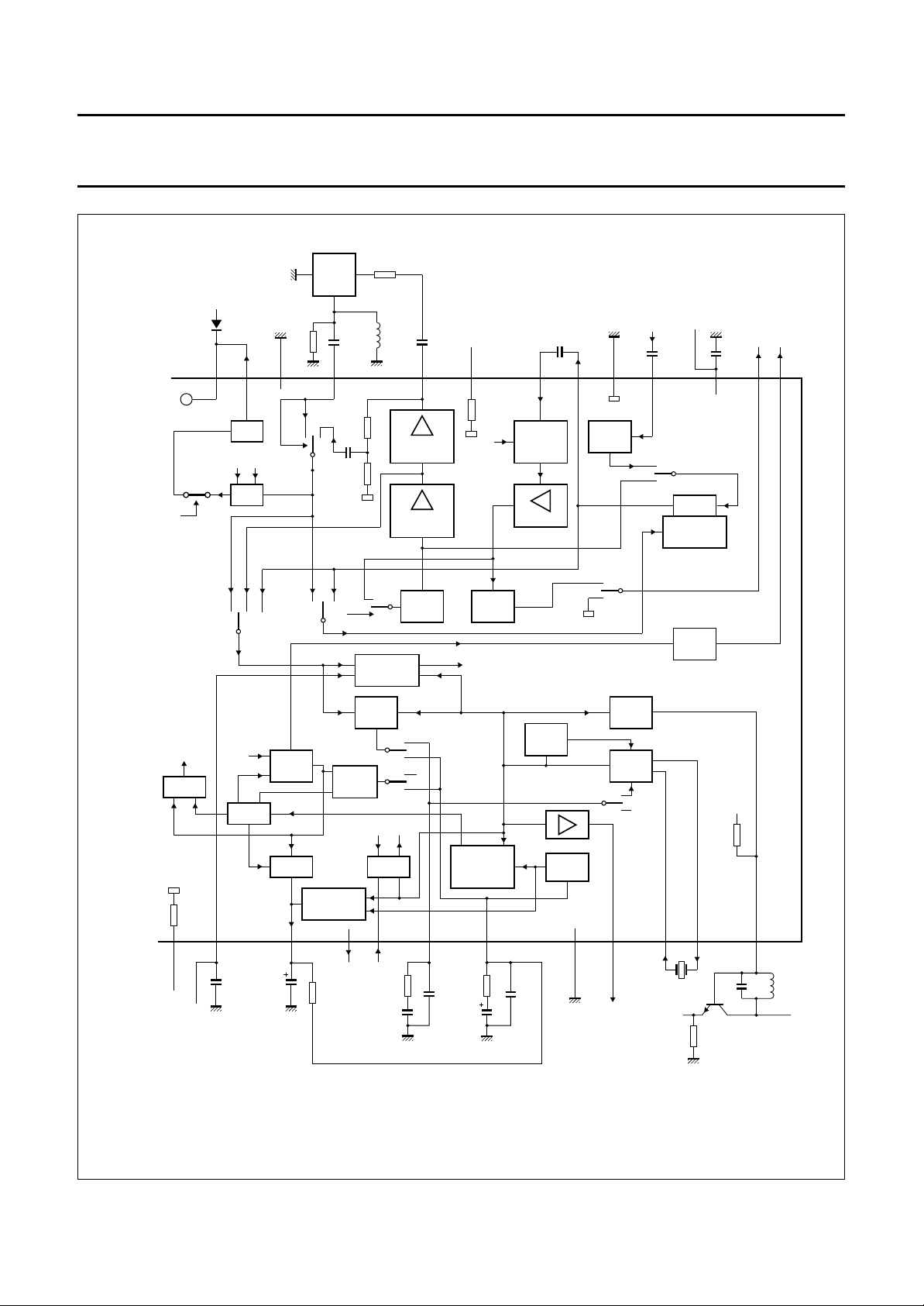
BLOCK DIAGRAM
handbook, full pagewidth
LPNC
GND(Y)
C
CCD
1.3
kΩ
10
µF
47
nF
52 51 50 49 48 47 46 45 44 43 42 41 40
VTC
1HDL
CCD
CCD
AGC
CLAMP
2
1 µF
VFC
50 kΩ
C
YNR
SS
CLAMP
1
YNR
PROCESSOR
22 nF
SYNC
SYNC
SEPARATOR
DOP
MIXER
YNR
CVBSI
C
AGC
4.7 µF 4.7 µF
HSS
AGC
AGC
DETECTOR
CLPA
Y/C
MIXER
to BPF 4.43
REC
PB
SCL
REC
LPF
TDA9725
0.1
µF
V
CC(Y)
22
10
µH
µF
A
CVBSO
CHI
PB
NOISE
CLIP
50
kΩ
CHARACTER
INSERT
EDIT
EDIT
50 kΩ
1.6 V
12 34 5 6 7 8 9 10 11 12 13 14
4.7
µF
(1)
PCTL
TP2
CDEV
EDIT
25 kΩ
DEVIATION/PLAYBACK
DETECTOR
ME
SQPB
1 kΩ
270 Ω
1 nF
SQPB
5%
NFB
NOISE
CANCELLER
1
PICTURE
to pin 6
CLPB
W/DC
to CLP3
22
nF
C
CLP3
CLAMP
DEVIATION
CONTROL
REC
PB
MODULATOR
0.1 µF
C
F0E
NLDE
YLPF
NLE
REC
PB
3
470 Ω
680 pF
peaking
DTE
SQPB
FM DEMODULATOR
SUBLPF
MDEBMDECMEO
1.5 kΩ1.5 kΩ
5%
f
PROCESSOR
0.1
µF
PB
REC
PB
TDA9725
2.5 dB
0
DOUBLE
LIMITER
PB
1 kΩ
FMO
V
CC(FM)
DROP-OUT
DETECTOR
ENVELOPE
DETECTOR
50 kΩ
PTR
pin 14
HIGH
0.01
µF
FM
AGC
FMI
GATE
C
FMA
DOP
0.33
µF
MGB694
(1) Low leakage current.
All capacitors for loop filter ±10%; all other capacitors+10%/−50%; all resistors ±5%; all inductors ±10%; unless otherwise specified.
Fig.1 Block diagram (continued in Fig.2).
1996 Oct 14 3
Page 4
Philips Semiconductors Product specification
Y/C automatic adjustment processor
(VHS standard)
handbook, full pagewidth
CK
H BLANK
AGCKP1
TP1
PBCI
A
PBCO
39 38 37 36 35 34 33 32 31 30 29 28 27
LPF
f
*
C
H/2
NAP
PB/SP
CF892
COMB
-15 dB
4
2
1.3
kΩ
CFI CDO
SEC
10 nF
270 Ω
3
15
µH
COMB
DRIVER
BURST
DOWN
SNP
50 kΩ
from
4 PHI
10 nF
BMI ACCO
BALANCED
MIXER
BURST UP
GND(C)
BPF
630
CFT
PB
REC
V
CC(C)
10 nF
ACC
ACC
DETECTOR
TDA9725
f
CTT
0.1
µF
H/2
REC
DETECTOR
PHI/PB
VXO
RECORD
AFC
FPC
BGP ROT
PB
BPF
4.43
REC
CK/FPC
REC
PB
REC
to BM
4 PHI : 4SLD
120
0.1 µF
(1)
kΩ
470
pF
LFVXO LFVCO
LPF
630
CK
f
sc
DIVIDER
SUBMIXER
LPF
680
Ω
1 µF
(1)
TDA9725
3rd
LOCK
VCO
47
nF
CK
X2
VXO
REC
PB
SEC
MUTE
XTALI XTALO
TEW 8H
f
sc
2 f
4.43619
MHz
sc
f
H/2
4.7 kΩ
V
8.0
kΩ
33
pF
CC(C)
PB
RECPB/LP
from pin 43
MUTE
MUTE
50 kΩ
15 16 17 18 19 20 21 22 23 24 25 26
ELS
CK
HSS
0.1
µF
: 40
(1)
1 µF
TIMER
FCO
FREQUENCY
DETECTOR
22 kΩ
V
MGB695
6.8
µH
CC(C)
(1) Low leakage current.
Fig.2 Block diagram (continued from Fig.1).
1996 Oct 14 4
Page 5
Philips Semiconductors Product specification
Y/C automatic adjustment processor
(VHS standard)
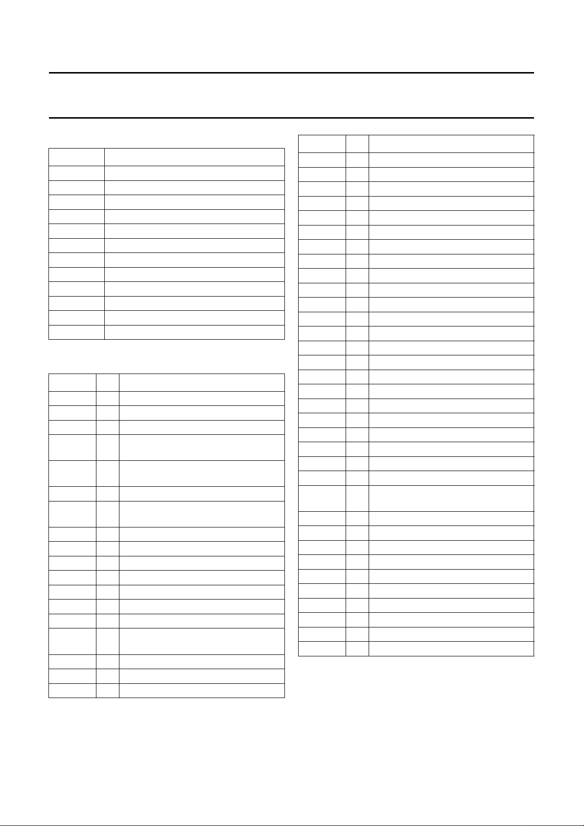
Table 1 Explanation of symbols in Figs 1 and 2
SYMBOL DESCRIPTION
AGCKP1 mode with shortened key pulse for AGC
BGP burst gate pulse
DOP dropout pulse
f
H
f
sc
HDL CCD charged coupled device with 1H delay
NLDE non-linear de-emphasis
NLEDTE non-linear emphasis/detail enhancer
ROT rotary pulse
VXO voltage controlled XTAL oscillator
YNR vertical noise reduction
YLPF luminance low-pass filter
PINNING
SYMBOL PIN DESCRIPTION
PCTL 1 picture control/edit switch input
CDEV 2 deviation/playback AGC detector input
TP2 3 test pin 2/correlation detector output
NFB
MEO
C
CLP3
C
F0E
MDEC 8 main de-emphasis output
MDEB 9 main de-emphasis and peaking output
V
CC(FM)
FMO 11 FM output
PTR 12 switch (PB/TRICK/REC)
FMI 13 playback FM input
C
FMA
ELS
CK 16 colour killer terminal
FCO 17 frequency correction output
BGP 18 burst gate pulse output
line frequency
subcarrier frequency (4.433619 MHz)
negative feedback input of main
4
emphasis
main emphasis output/white
5
clip/modulator input/SQPB selector
6 capacitor for clamp 3
storage capacitor for f0 processor
7
(record)/envelope detector (playback)
10 FM supply voltage
14 storage capacitor for FM AGC
PAL: switch (LP C*/LP/SP); NTSC:
15
switch (EP/LP/SP)
TDA9725
SYMBOL PIN DESCRIPTION
ROT 19 rotary pulse input
LFVXO 20 loop filter VXO
LFVCO 21 loop filter VCO
n.c. 22 not connected; note 1
f
sc
XTALI 24 VXO input from crystal
XTALO 25 VXO output to crystal
2f
sc
f
H/2
CTT 28 chrominance output to tape
V
CC(C)
CFT 30 playback chrominance input from tape
GND(C) 31 chrominance ground
ACCO 32 automatic chrominance control output
BMI 33 balanced mixer input
SNP 34 switch (SECAM/NTSC/PAL)
CDO 35 comb driver output
CFI 36 chrominance input from comb filter
TP1 37 test pin 1; note 1
PBCO 38 playback chrominance output
PBCI 39 playback chrominance input
V
CC(Y)
CVBSO 41 CVBS output
CHI 42 character insertion input (artificial
CVBSI 43 CVBS input
C
AGC
SYNC 45 sync separator push-pull output
C
SS
YNR 47 YNR switch
VFC 48 video input from 1HDL CCD
VTC 49 video output to 1HDL CCD
C
CCD
GND(Y) 51 luminance ground
LPNC 52 low-pass filter noise canceller
Note
1. It is recommended that this pin should be connected to
ground.
23 fsc output
26 2fsc output
27 f
H/2
output
29 chrominance supply voltage
40 luminance supply voltage
sync/black/white/through)
44 AGC detector capacitor
46 sync separator detector capacitor
50 storage capacitor for CCD AGC level
1996 Oct 14 5
Page 6
Philips Semiconductors Product specification
Y/C automatic adjustment processor
(VHS standard)
handbook, halfpage
PCTL
CDEV
C
CLP3
C
MDEC
MDEB
V
CC(FM)
C
LFVXO
LFVCO
XTALI
XTALO
TP2
NFB
MEO
F0E
FMO
PTR
FMI
FMA
ELS
CK
FCO
BGP
ROT
n.c.
f
2f
1
2
3
4
5
6
7
8
9
10
11
12
13
TDA9725
14
15
16
17
18
19
20
21
22
23
sc
24
25
26
sc
MGB693
52
51
50
49
48
47
46
45
44
43
42
41
40
39
38
37
36
35
34
33
32
31
30
29
28
27
LPNC
GND(Y)
C
CCD
VTC
VFC
YNR
C
SS
SYNC
C
AGC
CVBSI
CHI
CVBSO
V
CC(Y)
PBCI
PBCO
TP1
CFI
CDO
SNP
BMI
ACCO
GND(C)
CFT
V
CC(C)
CTT
f
H/2
TDA9725
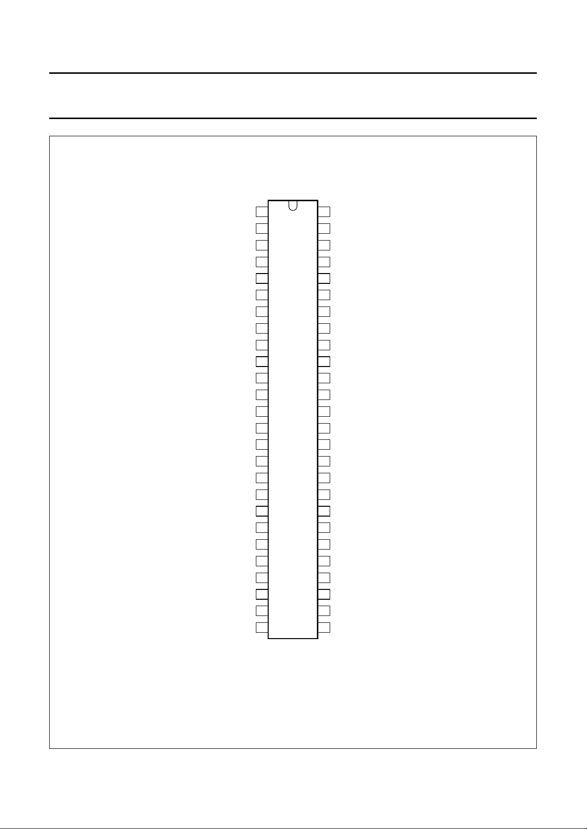
Fig.3 Pin configuration.
1996 Oct 14 6
Page 7
Philips Semiconductors Product specification
Y/C automatic adjustment processor
(VHS standard)
FUNCTIONAL DESCRIPTION
Record (REC)/electric to electric (EE) mode
UMINANCE
L
From input pin 43 the CVBS signal is fed via the automatic
gain control (AGC) and subclamp (SCL) to the output
pin 41. Instead of the controlled and clamped CVBS signal
it is also possible to switch (dependent on the level at
pin 42) white, black or sync-level to this pin. To eliminate
chrominance parts the CVBS signal is fed to the luminance
low-pass filter (YLPF) and to the sync separator stage.
The sync signal is available at pin 45. The signal is also fed
via vertical emphasis non-linear emphasis (NLE),
deviation control stage, main emphasis and white-dark clip
to the FM modulator. The FM signal is available at pin 11.
HROMINANCE
C
The chrominance signal is selected out of CVBS (from
pin 43) in BPF 4.43 MHz (band-pass filter) and controlled
in automatic chrominance control (ACC).
The chrominance signal is mixed with 5.06 MHz to
627 kHz and via LPF 627 kHz to the output pin 30.
TDA9725
Playback (PB)/video to video (VV) mode
LUMINANCE
The FM signal is fed via FM AGC and double limiter to the
controlled FM demodulator. After demodulation and
filtering in sub low-pass filter (SUBLPF) main
de-emphasis, YLPF and non-linear de-emphasis the
signal is fed to the vertical noise reduction (YNR) and in
parallel to the sync separator. The chrominance signal is
added in the Y/C mixer. The complete CVBS signal is
available at pin 41.
HROMINANCE
C
The 627 kHz chrominance signal coming from tape via
BPF 627 kHz and field ACC to the balanced mixer. Mixed
with 5.06 MHz the 4.43 MHz chrominance signal is fed via
comb driver stage to the external comb filter (pin 35) and
via internal conjugated complex (C*) stage and internal AC
coupling to the luminance part.
Record and playback
In both modes record (REC) and playback (PB) the
5.06 MHz mixer frequency is produced by the 20.24 MHz
voltage controlled oscillator (VCO) and a divide-by-four.
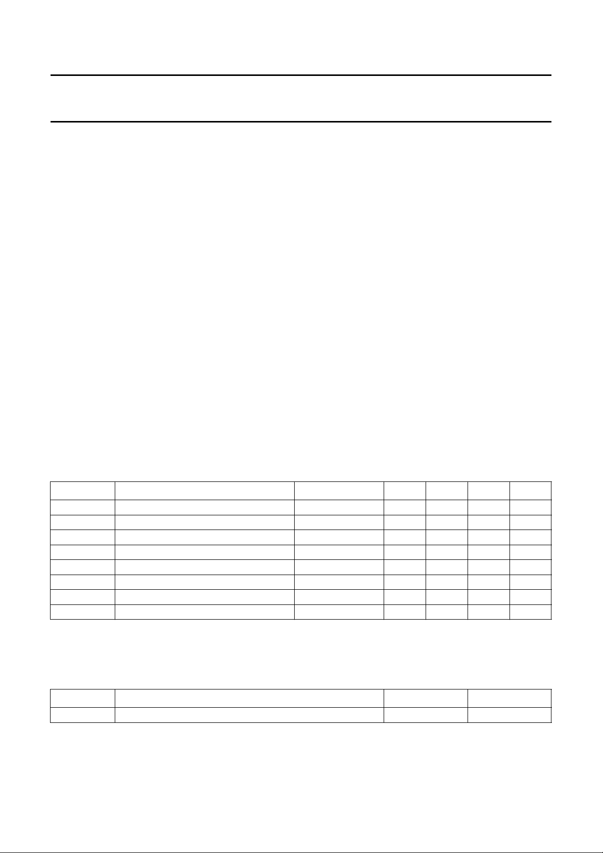
LIMITING VALUES
In accordance with the Absolute Maximum Rating System (IEC 134).
SYMBOL PARAMETER CONDITIONS MIN. TYP. MAX. UNIT
V
V
V
I
P
T
T
V
CC
I
n
I
tot
stg
amb
es
supply voltage 0 − 6.0 V
input voltage at pin 22 0 − 1.6 V
input voltage on all other pins 0 − V
CC
input current at pin 22 −−10 mA
total power dissipation −−1250 mW
storage temperature −25 − +150 °C
operating ambient temperature −20 − +70 °C
electrostatic handling for all pins note 1 −300 − +300 V
Note
1. Charge device model class B: discharging a 200 pF capacitor via a 0 Ω series resistor.
THERMAL CHARACTERISTICS
SYMBOL PARAMETER VALUE UNIT
R
th j-a
thermal resistance from junction to ambient in free air 43 K/W
V
1996 Oct 14 7
Page 8
Philips Semiconductors Product specification
Y/C automatic adjustment processor
TDA9725
(VHS standard)
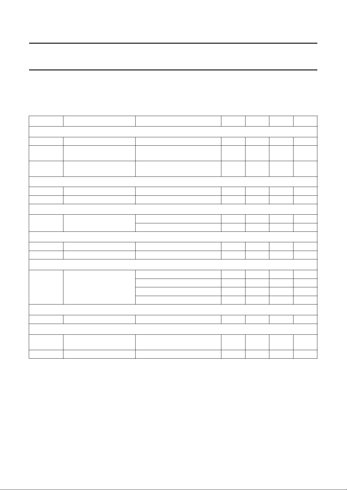
CHARACTERISTICS
VCC=5V; T
Luminance part: All amplitudes are VBS peak-to-peak values, unless otherwise specified.
Chrominance part: All amplitudes for P AL and NTSC are red values with 75% saturation and chrominance-to-burst ratio
of 2.2 : 1, unless otherwise specified.
SYMBOL PARAMETER CONDITIONS MIN. TYP. MAX. UNIT
Supplies
V
CC
I
PB
I
REC
FM SUPPLY (PIN 10)
I
PB
I
REC
CHROMINANCE SUPPLY (PIN 29)
I
CC(C)
UMINANCE SUPPLY (PIN 40)
L
I
PB
I
REC
Picture control/edit switch input (pin 1)
V
1
= +25 °C and typical application (see Figs 1 and 2), unless otherwise specified.
amb
supply voltage 4.5 5.0 5.5 V
current consumption
playback mode 140 170 200 mA
(I10+I29+I40)
current consumption
record mode 125 155 185 mA
(I10+I29+I40)
DC playback current − 22 − mA
DC record current − 12 − mA
DC supply current playback mode − 85 − mA
record mode − 85 − mA
DC playback current − 63 − mA
DC record current − 57 − mA
DC input voltage pin open-circuit − 1.6 − V
sharp picture 0 − 1.6 V
soft picture 1.6 − 3.2 V
edit mode 4.1 − 5.0 V
Deviation/playback AGC detector input (pin 2)
V
2
detection voltage 1.8 2.5 3.2 V
Test pin 2/correlation detector output (pin 3)
V
OH
HIGH level output voltage correlation of Y signal;
pin 37 LOW; RL≥ 10 kΩ
V
OL
LOW level output voltage non-correlation of Y signal − 0.1 0.5 V
1996 Oct 14 8
1.5 2.1 3.0 V
Page 9
Philips Semiconductors Product specification
Y/C automatic adjustment processor
TDA9725
(VHS standard)
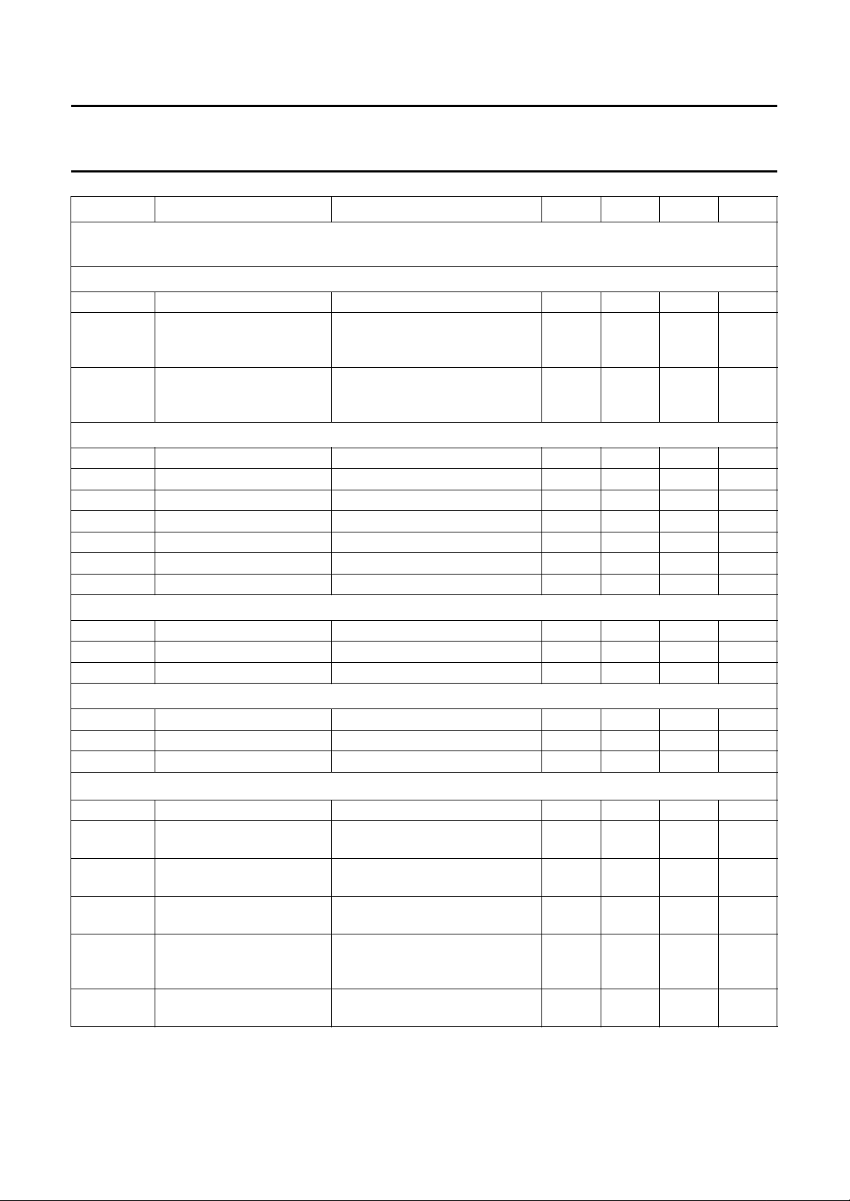
SYMBOL PARAMETER CONDITIONS MIN. TYP . MAX. UNIT
Negative feedback input of main emphasis (pin 4; open-base) and main emphasis
output/white-clip/modulator/SQPB selector (pin 5)
F
EEDBACK LOOP CLOSED (PIN 4 CONNECTED TO PIN 5; MAIN EMPHASIS OFF)
V
SY
V
oREC(p-p)
t
FRAMEDET
NON-LINEAR EMPHASIS/DETAIL ENHANCER; notes 2 and 3
RD1 response D1 −20 dB; f
RD2 response D2 −20 dB; f
RS1 response S1 −20 dB; f
RS1 response S2 −20 dB; f
RL1 response L1 −20 dB; f
RL2 response L2 −20 dB; f
RL3 response L3 0 dB; f
VERTICAL EMPHASIS
PL1 peak level 1 −30 dB recursive; note 4 3.5 4.3 5.3 dB
PL2 peak level 2 −20 dB recursive; note 4 3.5 4.0 4.5 dB
PL3 peak level 3 0 dB recursive 0 0.4 1.0 dB
EEDBACK LOOP NORMAL APPLICATION
F
DCL dark-clip level 50 60 70 %
WCL white-clip level 180 187 194 %
V
5
Record storage capacitor for f
V
I
V
NOR
V
OFF
V
NS
G
Eon
t
env
DC voltage level sync tip − 1.9 − V
record output voltage level;
standard output level
(peak-to-peak value)
time for correcting carrier
video/sync = 7/3;
450 500 550 mV
∆VCC= ±0.25 V;
T
= −10 to +70 °C
amb
HIGH during half picture 1; note 1 −−200 ms
interleave relationship to
half picture
= 500 kHz; SP; NORM 1.7 2.7 3.7 dB
i
= 2 MHz; SP; NORM 6.0 7.5 9.0 dB
i
= 500 kHz; SP; EDIT 1.0 1.7 2.4 dB
i
= 2 MHz; SP; EDIT 4.5 5.5 6.5 dB
i
= 500 kHz; LP 3.1 4.4 5.7 dB
i
= 2 MHz; LP 7.0 9.0 11 dB
i
= 2 MHz; LP 1.6 2.3 3.0 dB
i
SQPB input voltage playback mode 4.0 −−V
processor and playback storage capacitor for envelope detector (pin 7)
0
DC voltage record mode − 1.2 − V
DC voltage of normal mode playback mode;
= 350 mV (p-p); pin 14 HIGH
V
i
DC voltage of dropout
playback mode 0 − 1.3 V
2.3 3.3 4.0 V
correction (DOC) off mode
DC voltage at no input
playback mode 1.1 1.6 2.1 V
signal
envelope detector
switch-on level
(dropout active)
envelope detector operating
playback mode;
−13 −10 −7dB
0dB=Vi= 350 mV (p-p);
fi= 3.8 MHz; pin 14 HIGH
Ci= 0.1 µF 380 500 620 µs
time
1996 Oct 14 9
Page 10
Philips Semiconductors Product specification
Y/C automatic adjustment processor
TDA9725
(VHS standard)
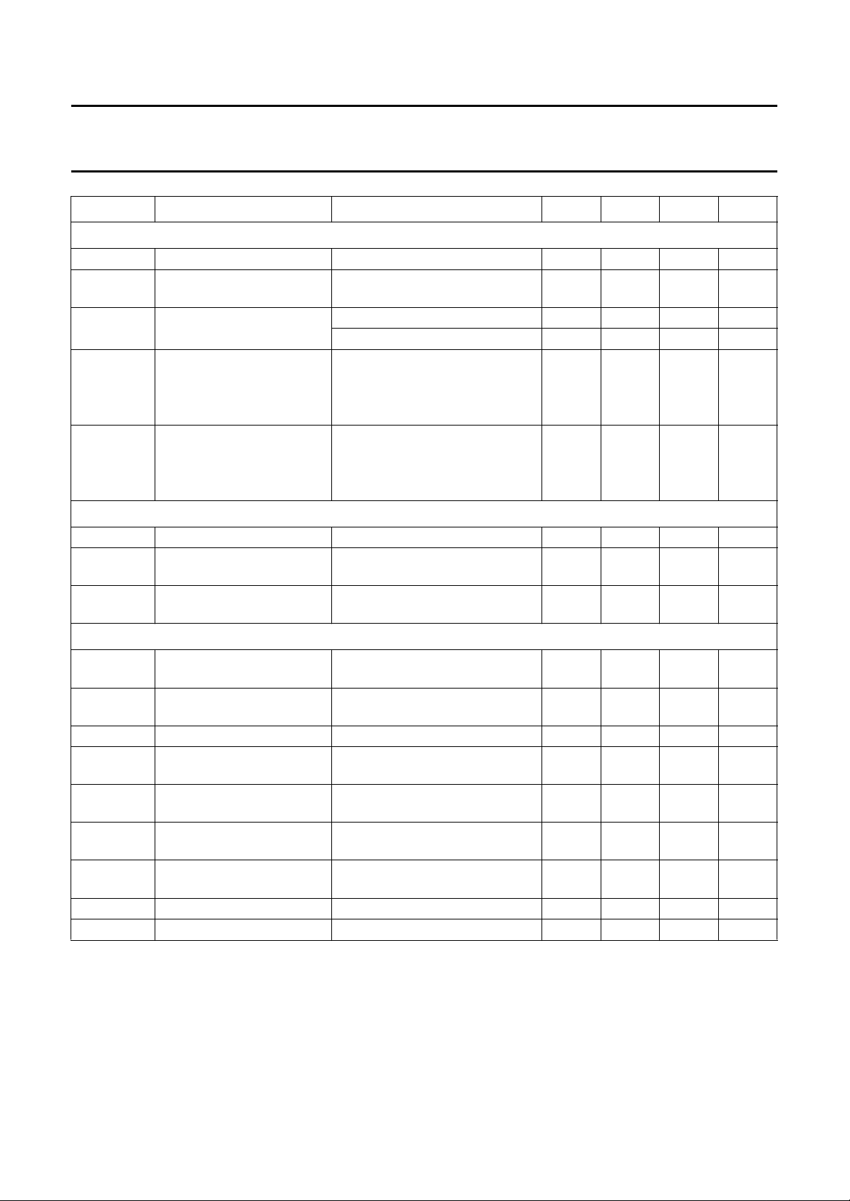
SYMBOL PARAMETER CONDITIONS MIN. TYP. MAX. UNIT
Main de-emphasis output (pin 8; open collector)
V
8
V
VID(p-p)
Φ
DEM
LIN1 demodulator linearity 1 VHS mode 0.97 1.0 1.03
LIN2 demodulator linearity 2 SQPB mode 0.90 1.0 1.07
Main de-emphasis and peaking output (pin 9)
V
9
V
VR(p-p)
α
DEM
DC output voltage fi= 3.8 MHz at VHS 2.9 3.4 3.9 V
video output voltage level
f
= 1 MHz 230 300 370 mV
DEV
(peak-to-peak value)
demodulator sensitivity VHS mode 0.23 0.3 0.37 V/MHz
SQPB mode 0.14 0.19 0.24 V/MHz
V05 MHz()V
-------------------------------------------------------------------V
4 MHz()V
0
9 MHz()V
V
0
-------------------------------------------------------------------V
7 MHz()V
0
4MHz()–
0
3MHz()–
0
7MHz()–
0
5MHz()–
0
DC output voltage fi= 3.8 MHz at VHS 1.1 1.6 2.1 V
reverse video voltage level
230 300 370 mV
(peak-to-peak value)
suppression of
40 −−dB
demodulated carrier
FM output (pin 11)
V
11
DC mean value output
voltage
V
11(p-p)
output voltage level
(peak-to-peak value)
f
sync
∆f
sync
sync output frequency V5=V
stability of sync output
frequency
f
∆f
dev
dev
frequency deviation V5=V
stability of frequency
deviation
∆f
H
L
rot
2
mod
carrier interleave frequency rotary pulse (pin 19) HIGH/LOW;
second harmonic distortion fi= 3.8 MHz −−50 −42 dB
modulator linearity 0.95 1.00 1.05
RL=1kΩ 2.9 3.2 3.5 V
RL=1kΩ 0.7 0.9 1.1 V
; V43= 0 dB 3.75 3.8 3.85 MHz
sync
∆VCC= ±0.25 V
or T
= −10 to +70 °C
amb
; V43= 0 dB;
white
−20 − +20 kHz
0.95 1.0 1.05 MHz
video/sync = 7/3
∆VCC= ±0.25 V
or T
= −10 to +70 °C
amb
−20 − +20 kHz
6.8 7.8 8.8 kHz
at SP and LP
1996 Oct 14 10
Page 11
Philips Semiconductors Product specification
Y/C automatic adjustment processor
TDA9725
(VHS standard)
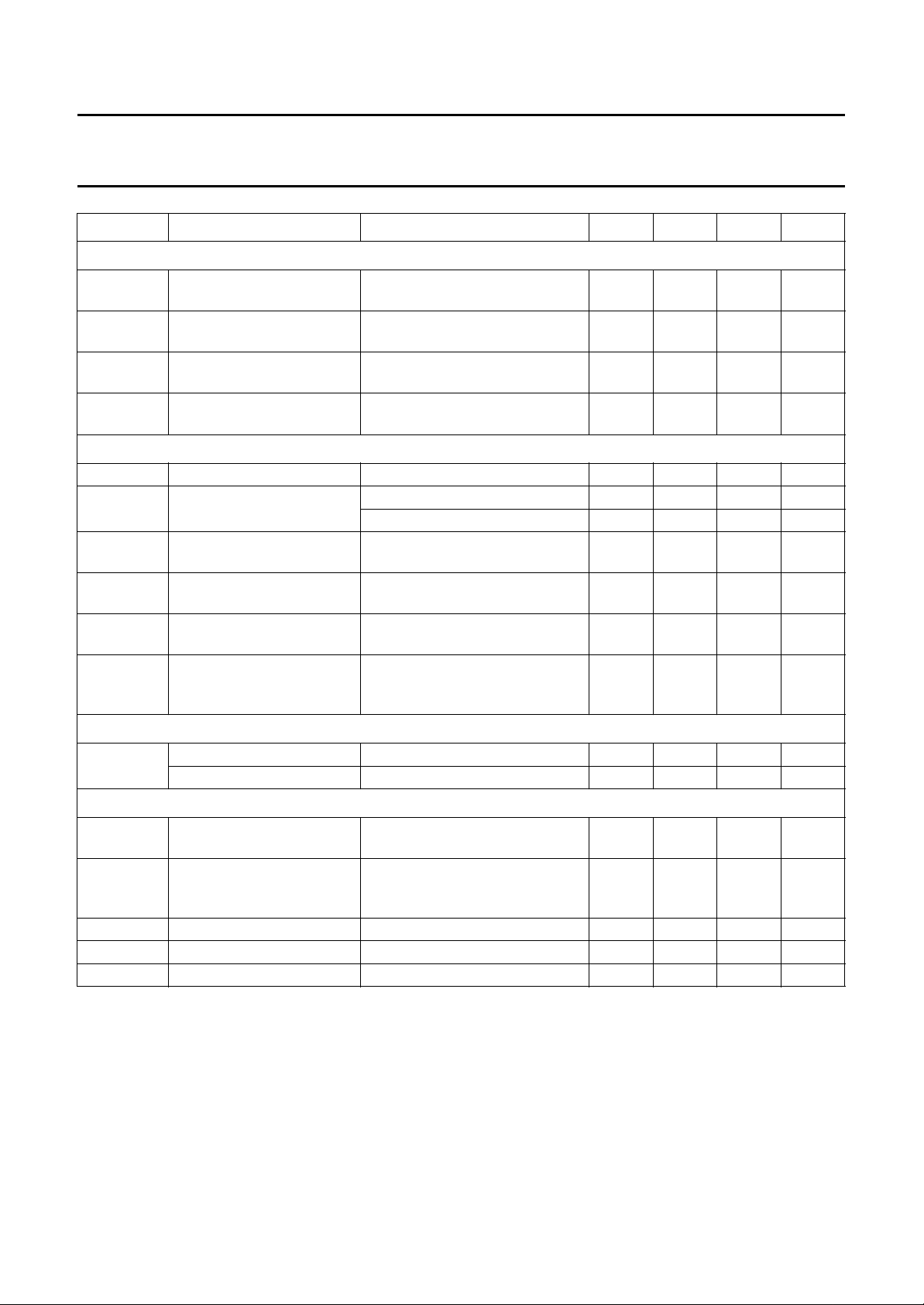
SYMBOL PARAMETER CONDITIONS MIN. TYP. MAX. UNIT
Switch: PB/TRICK/REC (pin 12)
R
I
internal resistance to
ground
V
PB
voltage range for active
playback mode
V
TR
voltage range for active
trick mode
V
REC
voltage range for active
record mode
Playback FM input (pin 13)
V
V
13
i(p-p)
DC voltage 1.7 2.2 2.7 V
input voltage level
(peak-to-peak value)
V
iBO(p-p)
boundary input voltage
(peak-to-peak value)
G
DOC
∆G
hys
G
Eon
DOC on level Vi= 350 mV (p-p); fi= 3.8 MHz;
DOC on/off hysteresis Vi= 350 mV (p-p); fi= 3.8 MHz;
envelope detector
switch-on level
FM AGC active 63 200 632 mV
FM AGC not active; pin 14 HIGH − 350 − mV
fi= 3.8 MHz; pin 14 HIGH 10 − 1000 mV
pins 7 and 14 HIGH
pins 7 and 14 HIGH
playback mode;
0dB=Vi= 350 mV (p-p);
fi= 3.8 MHz; pin 14 HIGH
40 50 60 kΩ
3.5 − 5V
1.75 − 3V
0 − 1.25 V
−18 −15 −12 dB
135dB
−13 −10 −7dB
Storage capacitor for FM AGC (pin 14; playback mode)
V
14
DC voltage AGC on 2.6 3.1 3.6 V
DC input voltage AGC off 4.3 − 5.0 V
Switch LP C*/LP/SP at PAL; EP/LP/SP at NTSC (pin 15)
R
I
internal resistance to
ground
V
C
input voltage for active C*
PAL 3.5 − 5V
(conjugated complex
chrominance signal)
V
E
V
L
V
S
input voltage for active EP NTSC 3.5 − 5V
input voltage for active LP 1.75 − 3V
input voltage for active SP 0 − 1.25 V
40 50 60 kΩ
1996 Oct 14 11
Page 12
Philips Semiconductors Product specification
Y/C automatic adjustment processor
TDA9725
(VHS standard)
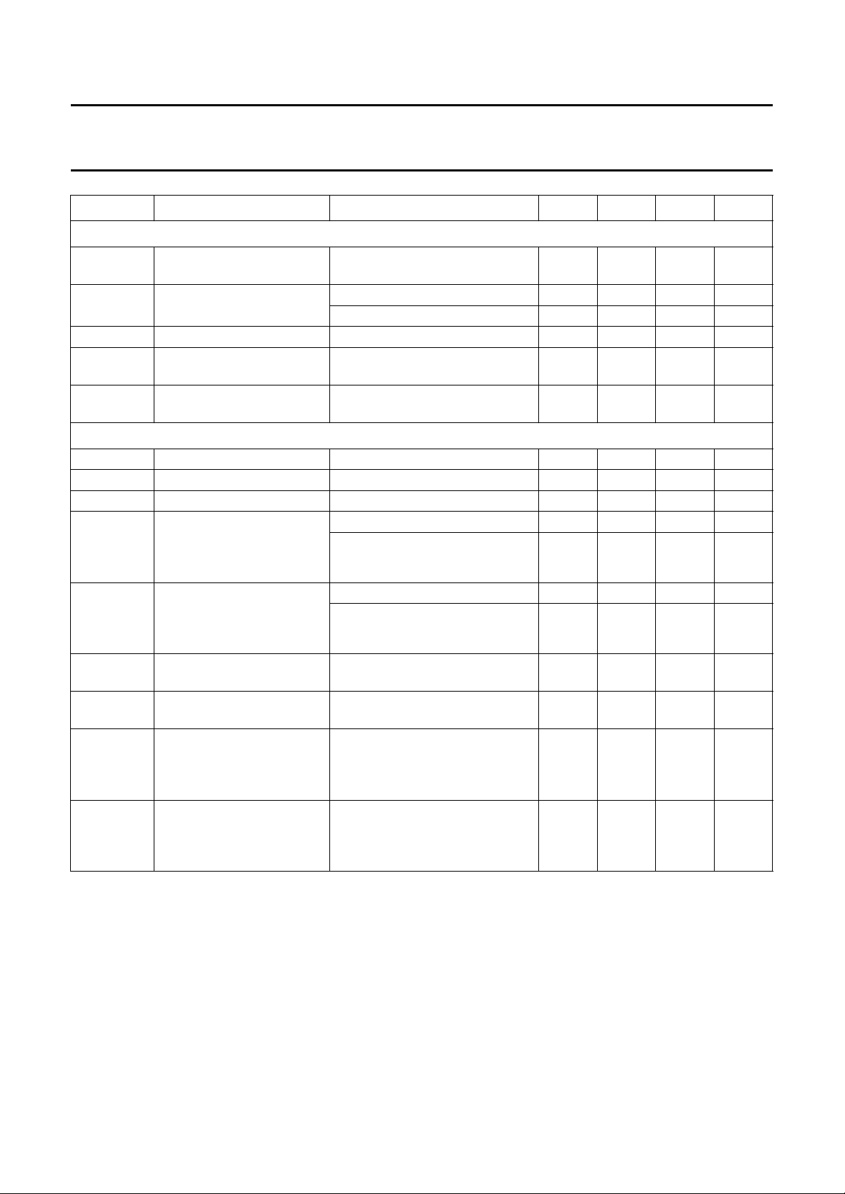
SYMBOL PARAMETER CONDITIONS MIN. TYP. MAX. UNIT
Colour killer terminal (pin 16)
V
V
V
CK
CK
NC
16
th
th
hys
DC voltage black and white luminance input without
input voltage forced colour off 0 − 1.5 V
threshold voltage colour on 2.0 2.2 2.4 V
colour killer threshold relative to nominal input;
colour killer hysteresis relative to nominal input;
Frequency correction output (pin 17)
V
17
I
oSLD
t
SLD
f
SLH
operating range 0.8 − 4.2 V
SLD output current SLD ±12 ±17 ±22 µA
SLD pulse duration SLD − 1 − t
start of detection at positive
frequency deviation
(referenced to fsc+N×fH at
pin 35; −I17)
f
SLL
start of detection at
negative frequency
deviation (referenced to
fsc+N×fH at pin 35; +I17)
I
ofDET
output current of frequency
detector
t
fDET
frequency detector pulse
duration
f
fDETH
start of detection at positive
frequency deviation
(referenced to fsc+N×fH at
pin 35; −I17)
f
fDETL
start of detection at
negative frequency
deviation (referenced to
fsc+N×fH at pin 35; +I17)
chrominance
forced colour on 3.0 − 4.3 V
V30= 110 mV (p-p)
V30= 110 mV (p-p)
SLD/PAL 1.0 2.0 3.0 kHz
SLD/NTSC 2.0 4.0 5.0 kHz
SLD/PAL −3.0 −2.0 −1.0 kHz
SLD/NTSC −5.0 −4.0 −2.0 kHz
FDET ±12 ±17 ±22 µA
FDET 68 73 78 µs
record mode 40 70 100 kHz
record mode −100 −70 −40 kHz
1.6 1.8 2.0 V
−25 −30 −35 dB
135dB
H
1996 Oct 14 12
Page 13
Philips Semiconductors Product specification
Y/C automatic adjustment processor
TDA9725
(VHS standard)
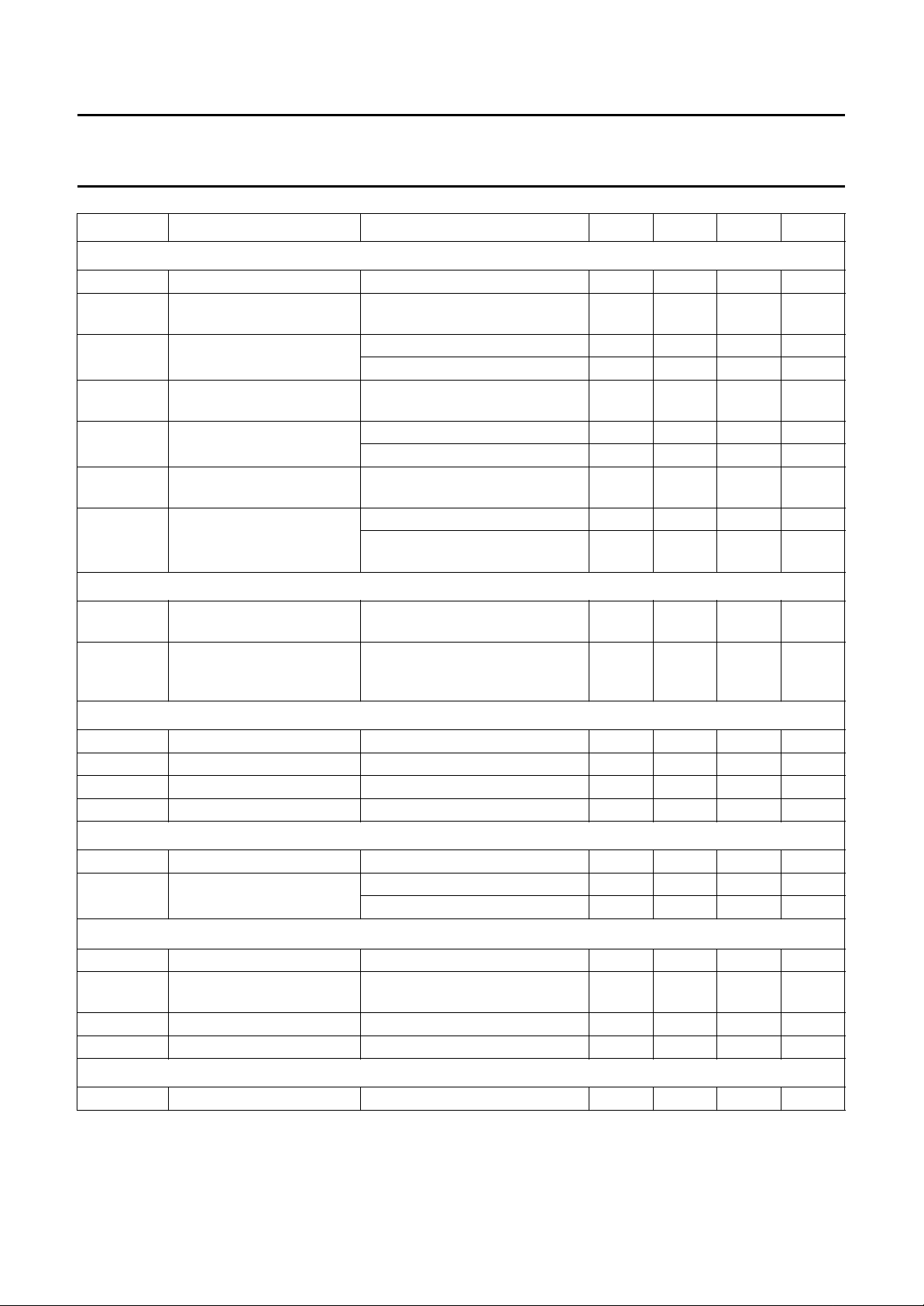
SYMBOL PARAMETER CONDITIONS MIN. TYP. MAX. UNIT
Burst gate pulse output (or sandcastle output; pin 18); note 5
t
BGP
t
BGS
V
O(L)
V
O(M)
V
O(H)
t
VBL(start)
t
VBL(stop)
Rotary pulse input (pin 19; open PNP base)
V
C2
V
C1
burst gate pulse duration 4.2 4.45 4.7 µs
start of burst gate beyond
3.25 3.5 3.75 µs
sync start at pin 45
LOW level DC output
voltage
medium level DC output
voltage
HIGH level DC output
voltage
vertical blanking of BGP
start
vertical blanking of BGP
stop
inactive; I18=1mA −−0.7 V
inactive; I
horizontal blanking;
10 kΩ connected to V
=0mA −−0.5 V
18
2.2 2.6 3.0 V
CC
BGP; I18= −0.4 mA 4.0 4.4 − V
BGP; I
referring to first equalisation
=0mA 4.6 −−V
18
− 0 − t
pulse in mid of line
referring to rotary transition 23 −−t
referring to last equalisation pulse
1 −−t
in mid of line
voltage for −90° phase
channel 2 0 − 2.25 V
rotation
voltage for non-rotation
channel 1 2.75 − 5V
(PAL) or +90° rotation
(NTSC)
H
H
H
Loop filter VXO (pin 20; record mode)
V
Φ
f
PI(U)
f
PI(L)
20
VXO
DC voltage 1 2.4 3.6 V
VXO sensitivity −1.6 −1.2 −0.8 Hz/mV
upper pull-in frequency 0.6 1.0 1.8 kHz
lower pull-in frequency −1.8 −1.0 −0.6 kHz
Loop filter VCO (pin 21)
V
21
Φ
VCO
output (pin 23)
f
sc
V
23
V
o(p-p)
DC voltage 1.3 2.1 2.9 V
VCO sensitivity fH related; record mode −34 −38 −42 kHz/V
DC output voltage 1.8 2.3 2.8 V
output signal voltage
(peak-to-peak value)
H
2
H
3
second harmonic distortion −−−25 dB
third harmonic distortion −−−20 dB
VXO input from crystal (pin 24); note 6
V
24
DC voltage 2.6 3.0 3.4 V
f
related; playback mode −1.3 −1.5 −1.7 MHz/V
sc
no load 500 600 700 mV
1996 Oct 14 13
Page 14
Philips Semiconductors Product specification
Y/C automatic adjustment processor
TDA9725
(VHS standard)
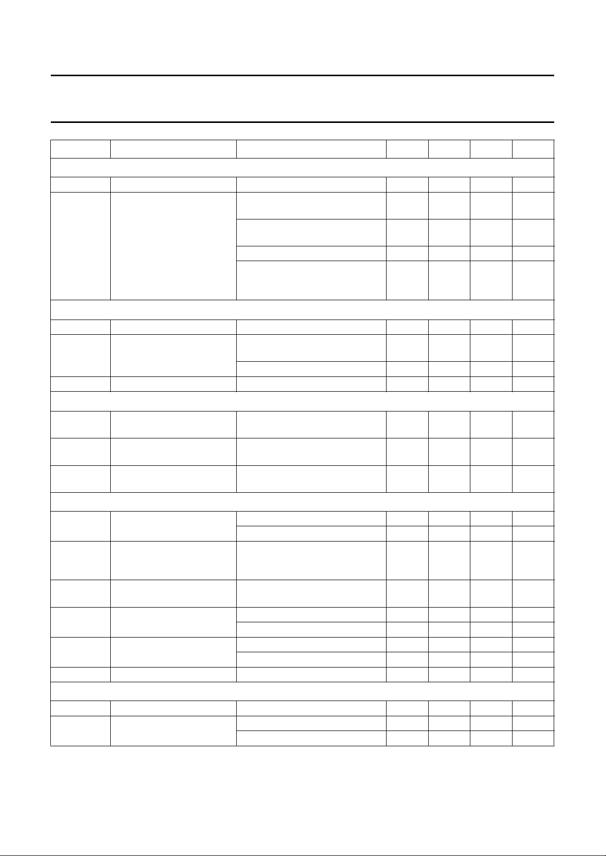
SYMBOL PARAMETER CONDITIONS MIN. TYP. MAX. UNIT
VXO output to crystal (pin 25)
V
25
∆f
osc
2f
output (pin 26)
sc
V
26
V
o
H
2
output; coupled to burst sequence (pin 27)
f
H/2
V
O(L)
V
O(H)
V
NTSC4.43
DC output voltage 2.9 3.3 3.7 V
deviation of oscillator
frequency
due to internal spread;
playback mode
video signal without burst;
−50 − +50 Hz
−1.4 − +1.4 kHz
record mode
no video signal; record mode −100 − +100 Hz
= 4.75 to 5.25 V;
V
CC
= −10 to +70 °C;
T
amb
−100 − +100 Hz
playback mode
DC output voltage 4.5 4.9 − V
output signal voltage 1.2 kΩ connected to VCC and
40 55 70 mV
emitter follower (EF)
tuned LC circuit to V
and EF 400 550 700 mV
CC
second harmonic distortion tuned LC circuit (Q > 20) and EF −−−30 dB
LOW level DC output
burst phase = +135°−−0.5 V
voltage
HIGH level DC output
burst phase = −135° 4.5 −−V
voltage
input level for forced
NTSC; playback mode −−1.5 V
NTSC 4.43 mode (no NAP)
Chrominance output to tape (pin 28); see Table 2
V
28
DC output voltage colour on 2.1 2.4 2.7 V
colour killer active − 0.1 0.3 V
V
o(p-p)
chrominance output signal
record mode; PAL 467 660 932 mV
voltage (N × fH)
(peak-to-peak value)
G
UP
SECAM-fOR burst related
SECAM 0.2 1.0 1.8 dB
to PAL burst
H
2
H
3
α
CK
second harmonic distortion V33=0dB −−−40 dB
=+6dB −−−35 dB
V
33
third harmonic distortion V33=0dB −−−40 dB
=+6dB −−−35 dB
V
33
colour killer suppression 40 −−dB
Playback chrominance input from tape (pin 30)
V
V
30
i(p-p)
DC voltage 1.7 2.2 2.7 V
input signal voltage
(peak-to-peak value)
chrominance + FM −−310 mV
chrominance 11 110 220 mV
1996 Oct 14 14
Page 15
Philips Semiconductors Product specification
Y/C automatic adjustment processor
TDA9725
(VHS standard)
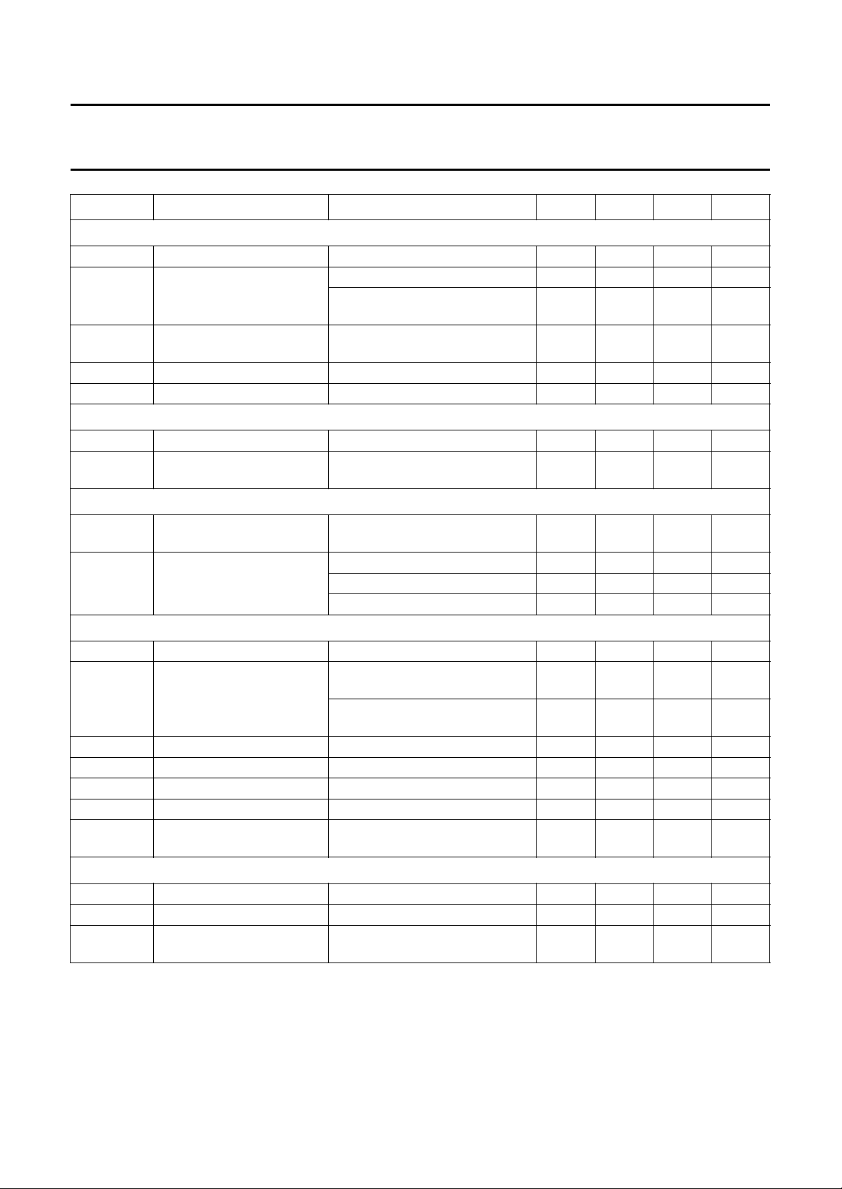
SYMBOL PARAMETER CONDITIONS MIN. TYP. MAX. UNIT
ACC output (pin 32); see Table 5
V
32
V
o(p-p)
∆G
o
H
2
H
3
Balanced mixer input (pin 33)
V
33
V
i(p-p)
Switch SECAM/NTSC/PAL (pin 34)
R
I
V
i
DC output voltage 1.75 2.25 2.75 V
controlled output signal
voltage
(peak-to-peak value)
deviation of output signal Vi= −15 dB/+6 dB;
Vi= 0 dB; record mode 370 460 550 mV
= 0 dB; playback mode; PAL;
V
i
350 440 530 mV
−15 dB comb filter
−1.0 − +1.0 dB
record and playback modes
second harmonic distortion nominal input and output signal −−−40 dB
third harmonic distortion nominal input and output signal −−−40 dB
DC voltage 1.6 1.9 2.2 V
nominal input signal voltage
− 440 − mV
(peak-to-peak value)
internal resistance to
40 50 60 kΩ
ground
input voltage active SECAM mode 3.5 − 5V
active NTSC mode 1.75 − 3V
active PAL mode 0 − 1.25 V
Comb driver output (pin 35); see Tables 3, 4 and 10
V
V
35
o(p-p)
DC output voltage record and playback modes 2.0 2.5 3.0 V
output signal voltage
(peak-to-peak value)
playback mode; NTSC;
−10 dB comb filter
playback mode; PAL/SECAM;
−15 dB comb filter
H
H
∆G
∆G
G
2
3
BD(S)
BD(E)
SECid
second harmonic distortion playback mode; 0 dB −−−40 dB
third harmonic distortion playback mode; 0 dB −−−40 dB
burst down playback mode; NTSC; SP −6.0 −5.0 −4.0 dB
burst down playback mode; NTSC; EP −5.0 −4.0 −3.0 dB
gain of output signal for
SECAM identification
record mode (ACC is not active)
from pin 43
Chrominance input from comb filter (pin 36)
V
V
V
GL
CCD
i(p-p)
DC voltage for glass comb AC coupled 3.2 4.0 4.8 V
DC voltage for CCD comb DC coupled 0 − 1.5 V
input signal voltage
PAL; NTSC − 120 − mV
(peak-to-peak value)
304 380 456 mV
540 675 810 mV
− 3.0 − dB
1996 Oct 14 15
Page 16
Philips Semiconductors Product specification
Y/C automatic adjustment processor
TDA9725
(VHS standard)
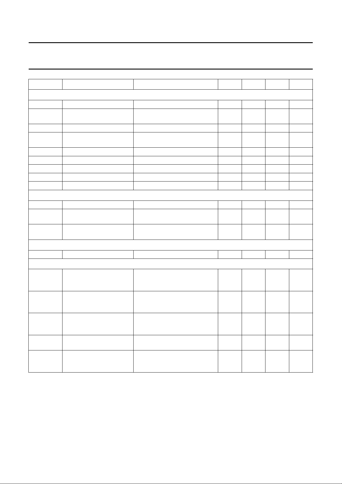
SYMBOL PARAMETER CONDITIONS MIN. TYP. MAX. UNIT
Playback chrominance output (pin 38; sync blanking is always active); see Table 6
V
38
V
o(p-p)
H
2
α
CK
∆V
C*
∆ϕ
C*
∆ϕ
NAP
α
2fsc
α
3fsc
Playback chrominance input (pin 39)
V
39
V
i(p-p)
V
th
DC output voltage 1.1 1.6 2.1 V
output signal voltage
V30= 110 mV (p-p) 270 325 420 mV
(peak-to-peak value)
second harmonic distortion V30= 110 mV (p-p) −−−40 dB
colour killer/pilot burst
suppression
colour killer or sync blanking
interval
40 −−dB
output amplitude deviation C to C*; V36= 120 mV (p-p) −1.5 0 +1.5 dB
output phase deviation C to C* or NAP line n to n + 1 −15 0 +15 °
phase for NAP burst NAP burst to −(B − Y) axis ±30 ±45 ±60 °
2fscsuppression C*; V36= 120 mV (p-p) 35 −−dB
3fsc suppression C*; V36= 120 mV (p-p) 18 25 − dB
DC voltage 1.7 2.0 2.3 V
input voltage
− 325 − mV
(peak-to-peak value)
threshold level of AGCKP1
record mode 2.6 3.0 3.4 V
(no reaction on copy guard)
CVBS output (pin 41); see Table 7
V
41
DC output voltage sync tip; RL= 2.1 kΩ 0.9 1.05 1.2 V
RECORD MODE
V
oREC(p-p)
record output voltage
(standard output level)
(peak-to-peak value)
∆V
oREC(p-p)
record output voltage level
stability
(peak-to-peak value)
V
o(p-p)
compressed sync output
voltage (200 IRE)
(peak-to-peak value)
G
CON
control characteristic of
AGC
∆V
CG
VHS standard
(signal amplitude for
copy guard tapes)
video/sync = 7/3; RL= 2.1 kΩ 2.03 2.14 2.25 V
∆VCC= ±0.25 V or
T
= −10 to +70 °C
amb
−40 − +40 mV
video/sync = 7.0/1.5 2.13 2.32 2.52 V
V43= 0.5 to 2.0 V (p-p) 0 0.2 1.0 dB
100% = typical output level;
35 − 48 %
copy guard 7 lines/field
1996 Oct 14 16
Page 17
Philips Semiconductors Product specification
Y/C automatic adjustment processor
TDA9725
(VHS standard)
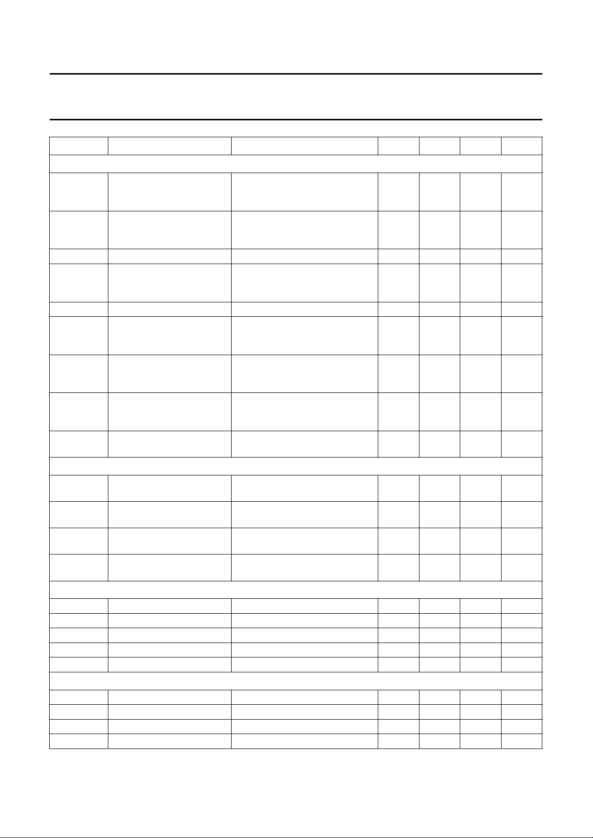
SYMBOL PARAMETER CONDITIONS MIN. TYP. MAX. UNIT
PLAYBACK MODE
V
oPB(p-p)
∆V
oPB(p-p)
V
NC
∆V
os
α
ct
t
att
t
rec
V
o(p-p)
∆G
CHROM
VERTICAL SYNCHRONIZATION PULSE/CHARACTER INSERT (RECORD AND PLAYBACK MODES)
∆V
ST
∆V
bl(p-p)
∆V
wh(p-p)
α
VIDEO
NON-LINEAR DE-EMPHASIS (PLAYBACK MODE); note 7
S1 response S1 −20 dB; f
S2 response S2 −20 dB; f
L1 response L1 −20 dB; f
L2 response L2 −20 dB; f
L3 response L3 0 dB; f
NOISE CANCELLER (PLAYBACK MODE); note 8
NC1 response NC1 −30 dB; f
NC2 response NC2 −30 dB; f
NC4 response NC4 0 dB; f
NCED response NCEDIT −30 dB; f
playback output voltage
(peak-to-peak value)
video/sync = 7/3; nominal FM
signal; RL= 2.1 kΩ; test: EE
2.03 2.14 2.25 V
without ME, MDE, peaking, YNR
playback output voltage
level stability
∆VCC= ±0.25 V or
T
= −10 to +70 °C
amb
−40 − +40 mV
(peak-to-peak value)
white noise clip level black-to-white = 100%; TRICK 115 135 150 %
offset voltage between
−25 − +25 mV
DOC mode and normal
mode
DOC switch crosstalk 0 dB = 2.0 V (p-p); fi= 1 MHz −−−40 dB
attack time of switching to
− 0.7 1.0 µs
DOC mode from normal
mode
recovery time of switching
4.0 5.0 6.0 µs
to normal mode from DOC
mode
chrominance output
V30= 110 mV (p-p) 1.0 1.2 1.4 V
voltage
(peak-to-peak value)
chrominance frequency
Vi=V39; fi=5to1MHz −2 − +2 dB
response
artificial sync tip level
V42= 0 to 5 V; playback mode −50 0 +50 mV
voltage offset
artificial black level voltage
V42= 5 to 3 V 0.58 0.68 0.78 V
(peak-to-peak value)
artificial white level voltage
V42= 5 to 2 V 1.7 1.9 2.05 V
(peak-to-peak value)
suppression of video at
40 −−dB
character insert
= 500 kHz; SP −2.9 −1.9 −0.9 dB
i
= 2 MHz; SP −6.5 −5.0 −3.5 dB
i
= 500 kHz; LP −6.5 −4.8 −3.0 dB
i
= 2 MHz; LP −10.2 −8.4 −6.7 dB
i
= 2 MHz; LP −4.8 −3.2 −1.8 dB
i
= 1 MHz; NORMAL −5.5 −3.5 −1.4 dB
i
= 2 MHz; NORMAL −15.0 −11.6 −8.0 dB
i
= 2 MHz; NORMAL −1.3 −0.3 +0.7 dB
i
= 2 MHz; EDIT −5.0 −3.4 −1.8 dB
i
1996 Oct 14 17
Page 18
Philips Semiconductors Product specification
Y/C automatic adjustment processor
TDA9725
(VHS standard)
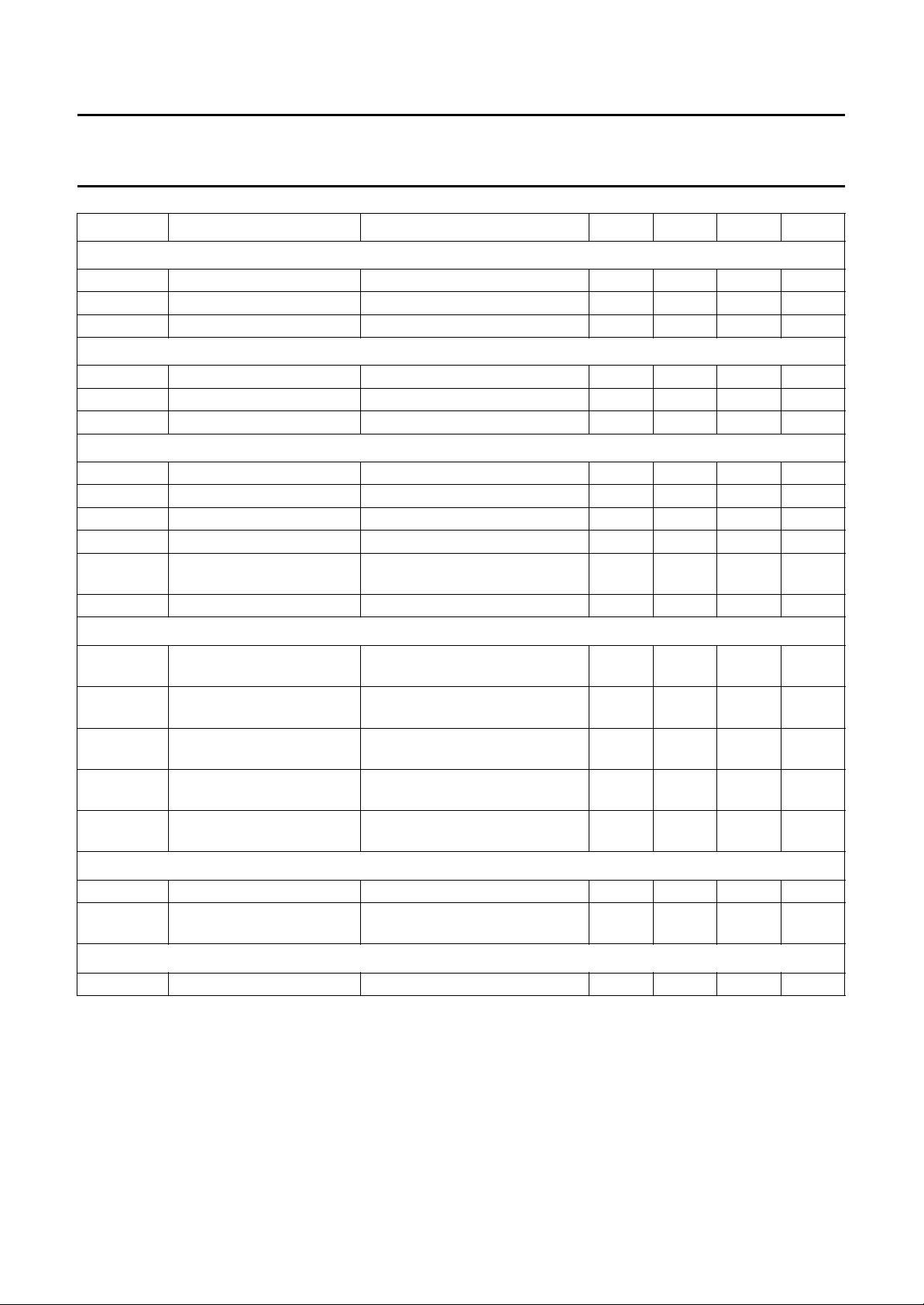
SYMBOL PARAMETER CONDITIONS MIN. TYP. MAX. UNIT
LINE NOISE CANCELLER (YNR WEAK; PLAYBACK MODE); note 9
LNC1 depth 1 −30 dB non-recursive −7.0 −5.5 −4.5 dB
LNC2 depth 2 −20 dB non-recursive −4.3 −3.3 −2.3 dB
LNC3 depth 3 0 dB non-recursive −1.0 −0.2 0 dB
ERTICAL NOISE CANCELLER (YNR STRONG; PLAYBACK MODE); note 9
V
VNC1 depth 1 −30 dB recursive −10.0 −8.5 −7.5 dB
VNC2 depth 2 −20 dB recursive −9.0 −7.5 −6.5 dB
VNC3 depth 3 0 dB recursive −1.8 −0.4 0 dB
ICTURE CONTROL; (note 10)
P
PC1 response 1 (sharp) V
PC2 response 2 (sharp) V
PC3 response 3 (soft) V
PC4 response 4 (soft) V
PC5 response 5 (centre) pin 1 open-circuit or > 4.1 V;
t
d
delay time pin 1 open-circuit; fi= 0.1 MHz 185 210 235 ns
Character insert (artificial sync/black/white/through; pin 42)
R
i
internal resistance to
ground
V
AS
input voltage for artificial
sync (inserts sync level)
V
AB
input voltage for artificial
black (inserts black level)
V
AW
input voltage for artificial
white (inserts white level)
V
THR
input voltage for through
mode
=0V; fi= 0.5 MHz 0 0.5 1.0 dB
1
=0V; fi= 2 MHz 3.7 4.7 5.7 dB
1
= 3.2 V; fi= 0.5 MHz −2.3 −1.3 −0.8 dB
1
= 3.2 V; fi= 2 MHz −6.8 −5.8 −4.8 dB
1
−0.5 +0.0 +0.5 dB
= 2 MHz
f
i
V42=0to1.0V 405060kΩ
4.0 − 5.0 V
2.75 − 3.5 V
1.5 − 2.25 V
0 − 1.0 V
CVBS input (pin 43)
V
V
43
i(p-p)
DC voltage 2.35 2.75 3.15 V
CVBS input voltage
(peak-to-peak value)
AGC detector (pin 44)
V
44
detector voltage V43= 1 V (p-p) 1.8 2.5 3.2 V
1996 Oct 14 18
0.3 1.0 2.0 V
Page 19
Philips Semiconductors Product specification
Y/C automatic adjustment processor
TDA9725
(VHS standard)
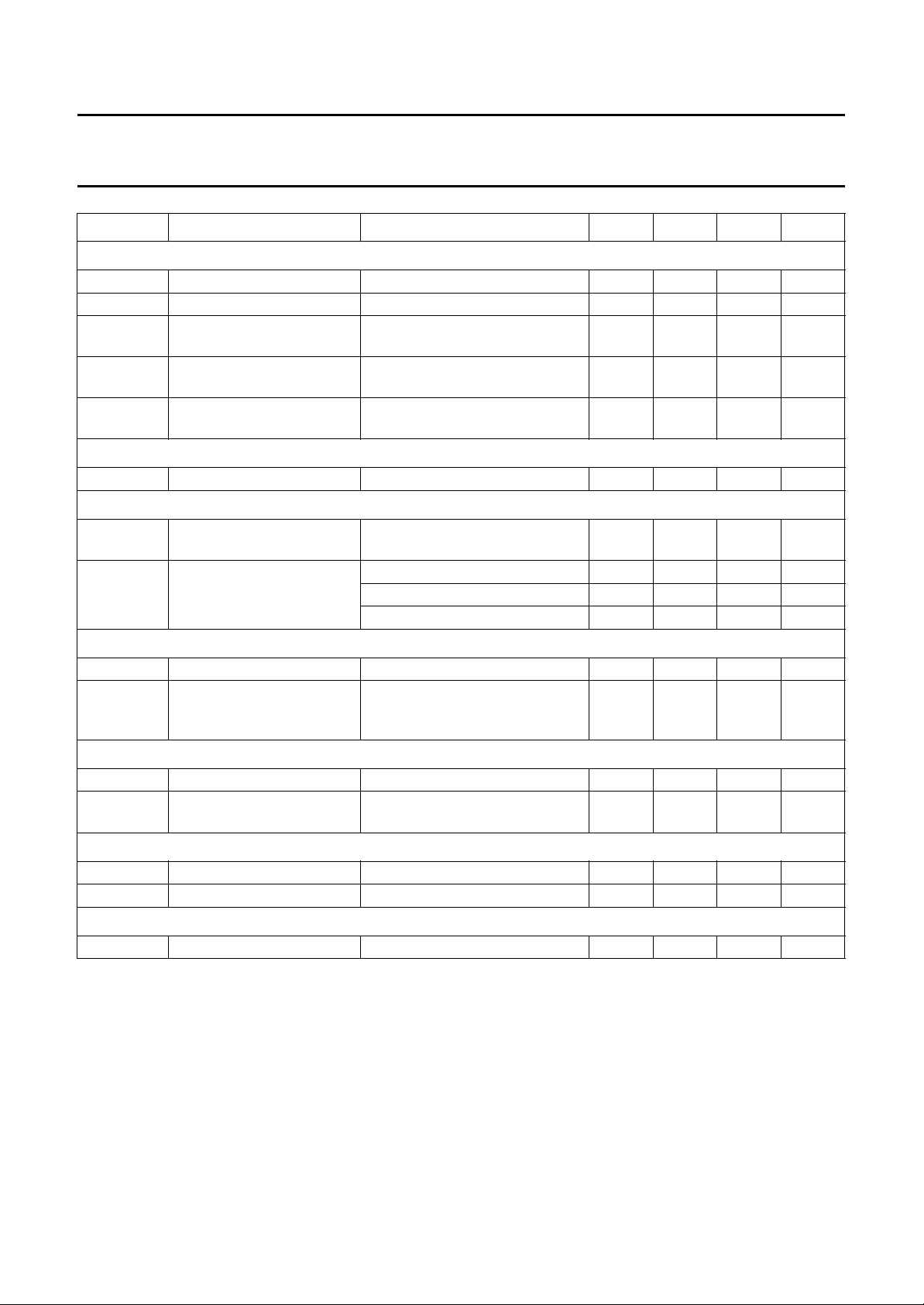
SYMBOL PARAMETER CONDITIONS MIN. TYP. MAX. UNIT
Sync separator push-pull output (pin 45)
V
O(H)
V
O(L)
t
dFE
t
dBE
Φ
sync
Sync separator detector (pin 46)
V
46
YNR switch (pin 47); see Table 11
R
I
V
47
HIGH level output voltage RL=2kΩto ground 4.5 −−V
LOW level output voltage RL=10kΩto V
CC
front edge delay time referenced to sync start pin 48;
−−0.3 V
600 750 900 ns
note 11
back edge delay time referenced to sync end pin 48;
100 350 600 ns
note 11
input sensitivity
sync-to-black = 100% 26 33 40 %
(slicing level for sync)
detector voltage 2.3 − 3.3 V
internal resistance to
40 50 60 kΩ
ground
input voltage YNR off mode 3.5 − 5.0 V
YNR1 mode 1.75 − 3.0 V
YNR2 mode 0 − 1.25 V
Video input from 1HDL CCD (pin 48)
V
V
48
i(p-p)
DC voltage 1.5 1.9 2.3 V
input voltage for constant
output signal at pin 49
(peak-to-peak value)
Video output to 1HDL CCD (pin 49)
V
V
oST
o(p-p)
sync tip output voltage 0.9 1.4 1.9 V
output voltage
CCD with −3 dB (record mode) 380 420 460 mV
(peak-to-peak value)
Storage capacitor for CCD level AGC (pin 50)
V
G
50
CCD
DC voltage 1.4 2.1 2.8 V
CCD gain control range 036dB
Low-pass filter input for noise canceller (pin 52)
V
52
DC voltage 1.0 1.2 1.4 V
178 283 449 mV
1996 Oct 14 19
Page 20

Philips Semiconductors Product specification
Y/C automatic adjustment processor
TDA9725
(VHS standard)
Notes to the characteristics
1. 50 Hz; rotary transition 8 to 4 lines beyond vertical pulse.
2. Test mode; YNR off; main emphasis off; V50= 1.5 V (minimum gain).
3. Input: V48= 143 mV sync and 0 dB = V48= 333 mV picture. Output: 0 dB = V5 picture at ≤50 kHz and given input
level.
4. Input: V43= 300 mV sync and 0 dB = V43= 700 mV picture. Output: 0 dB = V5 picture at 1, 2 and 3 × fH and given
input level.
5. Burst gate pulse output with no external components; sandcastle output with 10 kΩ resistor to VCC.
6. Crystal characteristics: TEW 8H:
f
= 4.433619 MHz ± 15 × 10−6; RS≤ 90 Ω; C1= 11 fF; L1= 117.14791 mH; C0= 2.6 pF.
nom
7. Input: V8= 90 mV sync and 0 dB = V8= 210 mV picture. Output: 0 dB = V41 at ≤50 kHz and given input level.
Noise canceller off; picture control centre; YNR off; measured with YLPF.
8. Input: V8= 90 mV sync and 0 dB = V8= 210 mV picture. Output: 0 dB = V41 at 100 kHz and given input level.
Picture control centre; NLDE off; YNR off. Pin 52: R = 1.3 kΩ; C = 47 nF (parasitic capacitance: 5 pF from
pin 52 to GND).
9. Input: V8= 90 mV sync and 0 dB = V8= 210 mV picture. Output: 0 dB = V41 at 1, 2 and 3 × fH and given input level.
Picture control at centre; NC off; NLDE off.
10. Input: V8= 90 mV sync and V8= 67 mV picture. Output: 0 dB = V41 at 100 kHz referring to YNRMIX signal at pin 3
of the same frequency. Noise canceller off; YNR off; NLDE off.
11. Input: V48= 143 mV sync; V50= 1.5 V; dropout or test mode forced DOC.
1996 Oct 14 20
Page 21
Philips Semiconductors Product specification
Y/C automatic adjustment processor
TDA9725
(VHS standard)
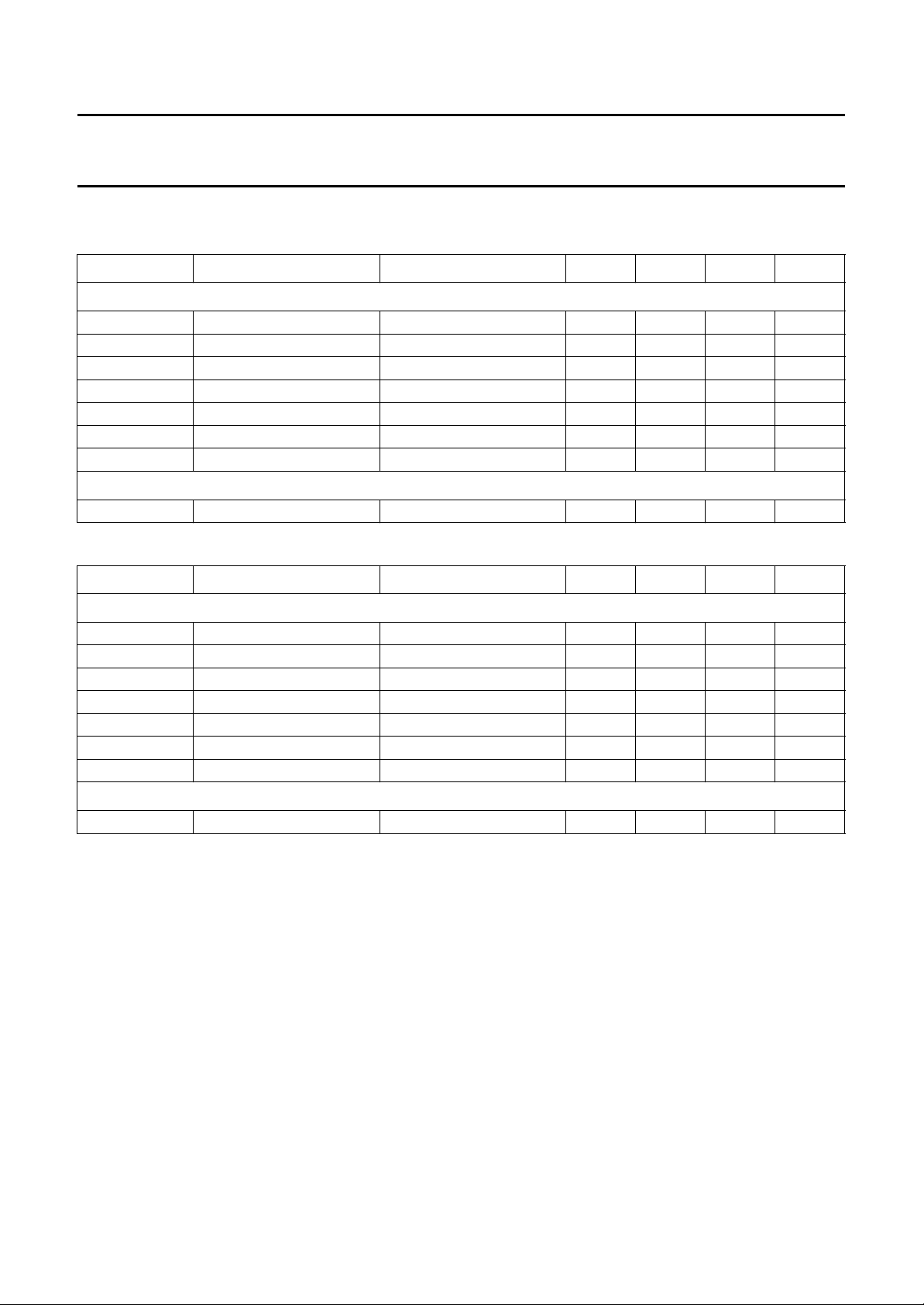
CHROMINANCE FILTER CHARACTERISTICS
Table 2 Low-pass filter 630 kHz; frequency response pin 33 to pin 28
SYMBOL PARAMETER CONDITIONS MIN. TYP. MAX. UNIT
PAL; NTSC/REC
∆G1 frequency response 1 G(1 MHz)/G(0.2 MHz) −4 −3 −2dB
∆G2 frequency response 2 G(1.5 MHz)/G(0.2 MHz) −9 −7 −5dB
∆G3 frequency response 3 G(2 MHz)/G(0.2 MHz) −10 −14 −18 dB
∆G4 frequency response 4 G(3 MHz)/G(0.2 MHz) −−−25 dB
∆G5 frequency response 5 G(4.43 MHz)/G(0.2 MHz) −−−40 dB
∆G7 frequency response 7 G(9.5 MHz)/G(0.2 MHz) −−−35 dB
t
d
SECAM; REC
∆G2 frequency response (2) G(1.5 MHz)/G(0.2 MHz) −5 −3 −1dB
Table 3 Band-pass filter 4.43 MHz at record mode; frequency response pin 43 to pin 35
SYMBOL PARAMETER CONDITIONS MIN. TYP. MAX. UNIT
group delay 1 fi= 0.63 MHz 295 335 375 ns
PAL; NTSC/REC
∆G1 frequency response 1 G(<2.7 MHz)/G(4.43 MHz) −−−22 dB
∆G2 frequency response 2 G(2.7 MHz)/G(4.43 MHz) −−−30 dB
∆G3 frequency response 3 G(3.93 MHz)/G(4.43 MHz) −3.8 −2.8 −1.8 dB
∆G4 frequency response 4 G(4.93 MHz)/G(4.43 MHz) −2.5 −1.5 −0.5 dB
∆G5 frequency response 5 G(6.2 MHz)/G(4.43 MHz) −−−30 dB
∆G6 frequency response 6 G(>6.2 MHz)/G(4.43 MHz) −−−15 dB
t
d
SECAM; REC
∆G7 frequency response 7 G(5.7 MHz)/G(4.43 MHz) −−−25 dB
group delay 1 fi= 4.43 MHz 410 450 490 ns
1996 Oct 14 21
Page 22
Philips Semiconductors Product specification
Y/C automatic adjustment processor
TDA9725
(VHS standard)
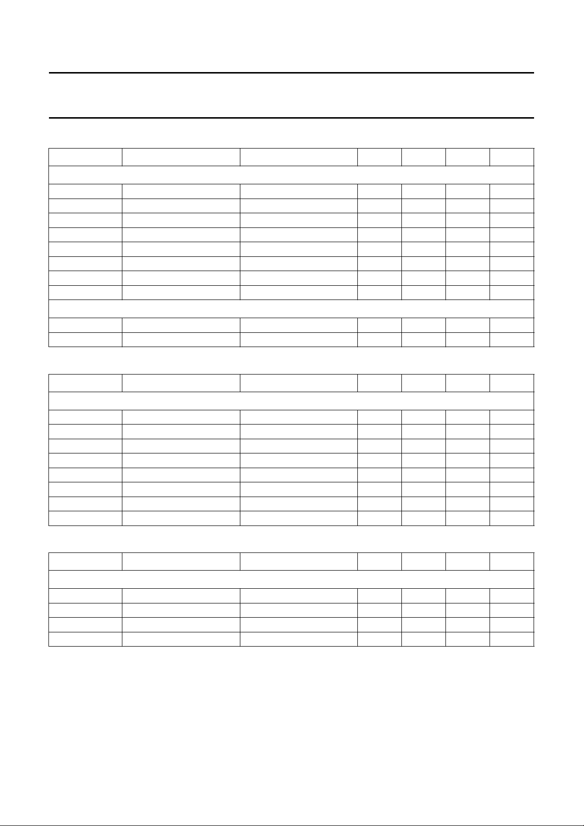
Table 4 Band-pass filter 4.43 MHz at playback mode; frequency response pin 33 to pin 35 (test mode)
SYMBOL PARAMETER CONDITIONS MIN. TYP. MAX. UNIT
PAL; NTSC/PB
∆G1 frequency response 1 G(<2.7 MHz)/G(4.43 MHz) −−−20 dB
∆G2 frequency response 2 G(2.9 MHz)/G(4.43 MHz) −−−30 dB
∆G3 frequency response 3 G(3.93 MHz)/G(4.43 MHz) −3.7 −2.7 −1.7 dB
∆G4 frequency response 4 G(4.93 MHz)/G(4.43 MHz) −3.9 −2.9 −1.9 dB
∆G5 frequency response 5 G(5.7 MHz)/G(4.43 MHz) −−30 −25 dB
∆G6 frequency response 6 G(6 MHz)/G(4.43 MHz) −−−22 dB
∆G7 frequency response 7 G(>6 MHz)/G(4.43 MHz) −−−15 dB
t
d
SECAM; PB
∆G8 frequency response 8 G(1.9 MHz)/G(4.43 MHz) −−30 −22 dB
∆G9 frequency response 9 G(5.5 MHz)/G(4.43 MHz) −−30 −22 dB
Table 5 Band-pass filter 630 kHz; frequency response pin 30 to pin 32 (test mode)
group delay 1 fi= 4.43 MHz 445 485 525 ns
SYMBOL PARAMETER CONDITIONS MIN. TYP. MAX. UNIT
PB
∆G1 frequency response 1 G(<100 Hz)/G(630 kHz) −−−20 dB
∆G2 frequency response 2 G(100 kHz)/G(630 kHz) −7 −5 −3dB
∆G3 frequency response 3 G(930 kHz)/G(630 kHz) −3 −2 −1dB
∆G4 frequency response 4 G(1.5 MHz)/G(630 kHz) −−15 −10 dB
∆G5 frequency response 5 G(2.3 MHz)/G(630 kHz) −−−40 dB
∆G6 frequency response 6 G(>2.4 MHz)/G(630 kHz) −−−33 dB
t
d
∆t
d
Table 6 Low-pass filter C*; frequency response pin 36 to pin 38
SYMBOL PARAMETER CONDITIONS MIN. TYP. MAX. UNIT
PB; C
∆G1 frequency response 1 G(5 MHz)/G(2 MHz) 0 −1.5 −3dB
∆G2 frequency response 2 G(13.3 MHz)/G(2 MHz) −18 −25 − dB
∆G3 frequency response 3 G(>13.3 MHz)/G(2 MHz) −18 −−dB
t
d
group delay 1 fi= 630 kHz; pin 36 normal 710 750 790 ns
group delay 4 difference V36=4to1V −250 −210 −170 ns
group delay 1 fi= 4.43 MHz 65 95 125 ns
1996 Oct 14 22
Page 23
Philips Semiconductors Product specification
Y/C automatic adjustment processor
TDA9725
(VHS standard)
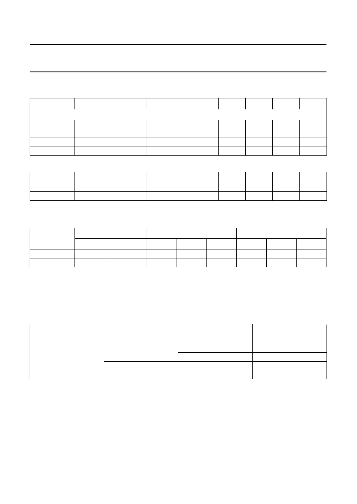
LUMINANCE FILTER CHARACTERISTICS
Table 7 Low-pass filter 4.43 MHz; frequency response pin 43 to pin 3 (test mode)
SYMBOL PARAMETER CONDITIONS MIN. TYP. MAX. UNIT
REC
∆G1 frequency response 1 G(2 MHz)/G(0.2 MHz) −1.0 +0.5 +1.5 dB
∆G2 frequency response 2 G(3 MHz)/G(0.2 MHz) −2.5 −1.0 +0.5 dB
∆G3 frequency response 3 G(4.43 MHz)/G(0.2 MHz) −−40 −30 dB
t
d
Table 8 Sub-low-pass filter; frequency response from FM demodulator to pin 9
SYMBOL PARAMETER CONDITIONS MIN. TYP. MAX. UNIT
∆G1 frequency response 1 G(3 MHz)/G(0.2 MHz) −4.5 −20 dB
∆G2 frequency response 2 G(6 MHz)/G(0.2 MHz) −−25 −15 dB
Sensitivity
Table 9 Sensitivity of PB APC (multiplication factor for phase detector sensitivity)
group delay 1 fi= 0.2 MHz 710 750 790 ns
PROGRAM
PAL NTSC/NAP NTSC4.4
SP LP SP LP EP SP LP EP
NORM 2 1
TRICK 2 1
(2)
(1)(2)
2
2
(1)(2)
(1)(2)
2
2
(1)(2)
(1)(2)
2
2
(1)(2)
(1)(2)
4
2
(1)
(1)(2)
2
2
(1)(2)
(1)(2)
Notes
1. No alternating reference for APC loop.
2. Comb filter is inside the APC loop.
Burst down logic Table 10 Burst down logic
MODE SYSTEM BURST DOWN
Playback NTSC SP ON (−5.0 dB)
LP OFF
EP ON (−4.0 dB)
PAL OFF
SECAM OFF
(1)(2)
2
(1)(2)
2
1996 Oct 14 23
Page 24
Philips Semiconductors Product specification
Y/C automatic adjustment processor
TDA9725
(VHS standard)
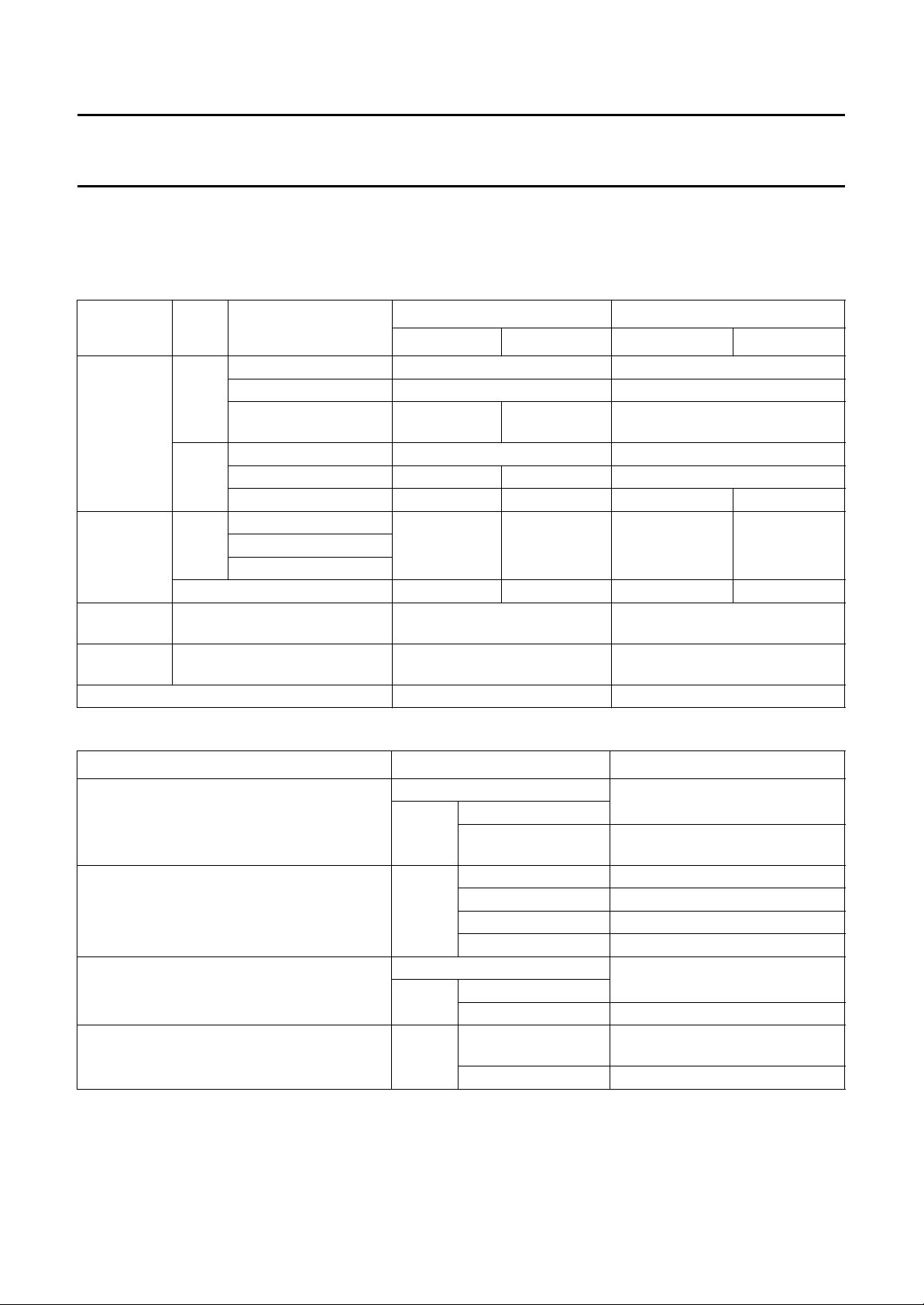
OPERATION MODE
Table 11 Operation mode (PART 1)
For PAL RECORD, SECAM ME RECORD, PAL PLAYBACK, SECAM ME PLAYBACK and NTSC PLAYBACK.
EP mode at NTSC PLAYBACK activates the same functions as LP mode.
FILTER MODE CONDITIONS
YNR REC YNR off; pin 47 HIGH OFF OFF
YNR 1; pin 47 medium OFF OFF
YNR 2; pin 47 LOW OFF vertical
PB YNR off; pin 47 HIGH OFF OFF
YNR 1; pin 47 medium VNC (strong) LNC (weak) OFF
YNR 2; pin 47 LOW LNC (weak) VNC (strong) OFF LNC (weak)
NLE
NLDE
Noise
canceller
Picture
control
FM carrier interleave ON ON
REC YNR off; pin 47 HIGH NLE(C) + DTE NLE(D) NLE(C) NLE(D)
YNR 1; pin 47 medium
YNR 2; pin 47 LOW
PB NLDE(C) NLDE(D) NLDE(C) NLDE(D)
PB ON WEAK
PB ON OFF
EDIT OFF EDIT ON
SP LP SP LP
OFF
emphasis
Table 12 Operation mode (PART 2)
FUNCTION CONDITIONS OPERATION
Clamps REC ON
PB NORM
dropout;
maximum 128 lines
Character insert REC orPBVIDEO; pin 42 LOW through
WHITE; pin 42 = M1 white level (85%)
BLACK; pin 42 = M2 black level
SYNC; pin 42 HIGH sync tip level
Search noise clip REC OFF
PB NORM
TRICK ON
SQPB PB VHS; pin 5
open-circuit
SQPB; pin 5 HIGH SQPB
OFF
VHS
1996 Oct 14 24
Page 25
Philips Semiconductors Product specification
Y/C automatic adjustment processor
(VHS standard)
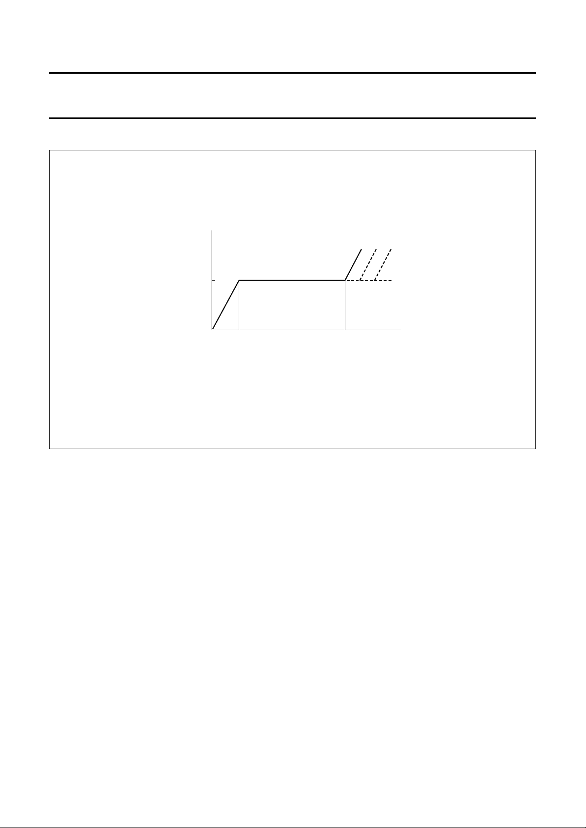
Automatic chrominance control (ACC) characteristics
handbook, halfpage
V
o(p-p)
(mV)
440
MBG150
+ 6V
(dB)− 22
i
TDA9725
0 dB is equivalent to 110 mv (p-p) at pin 30.
Fig.4 ACC characteristics.
1996 Oct 14 25
Page 26
Philips Semiconductors Product specification
Y/C automatic adjustment processor
(VHS standard)
MBG140
50 kΩ
1
Z INTERNAL CIRCUIT
50 kΩ
1.6 V
+
/I
E
T
++
100 Ω/
1.3 kΩ
TDA9725
MBG145
1.3 kΩ
1.6 kΩ 1.3 kΩ
100 Ω
2
80 µA 2.7 µA
1.6 V to 3.2 V soft
4.1 V to 5.0 V EDIT
WAVEFORM
EE VV
(V)
DC
1.6 4.1 V to 5.0 V EDIT 0 V to 1.6 V sharp
2.5 V
PIN NAME
(DESCRIPTION)
PIN
INTERNAL CIRCUITRY
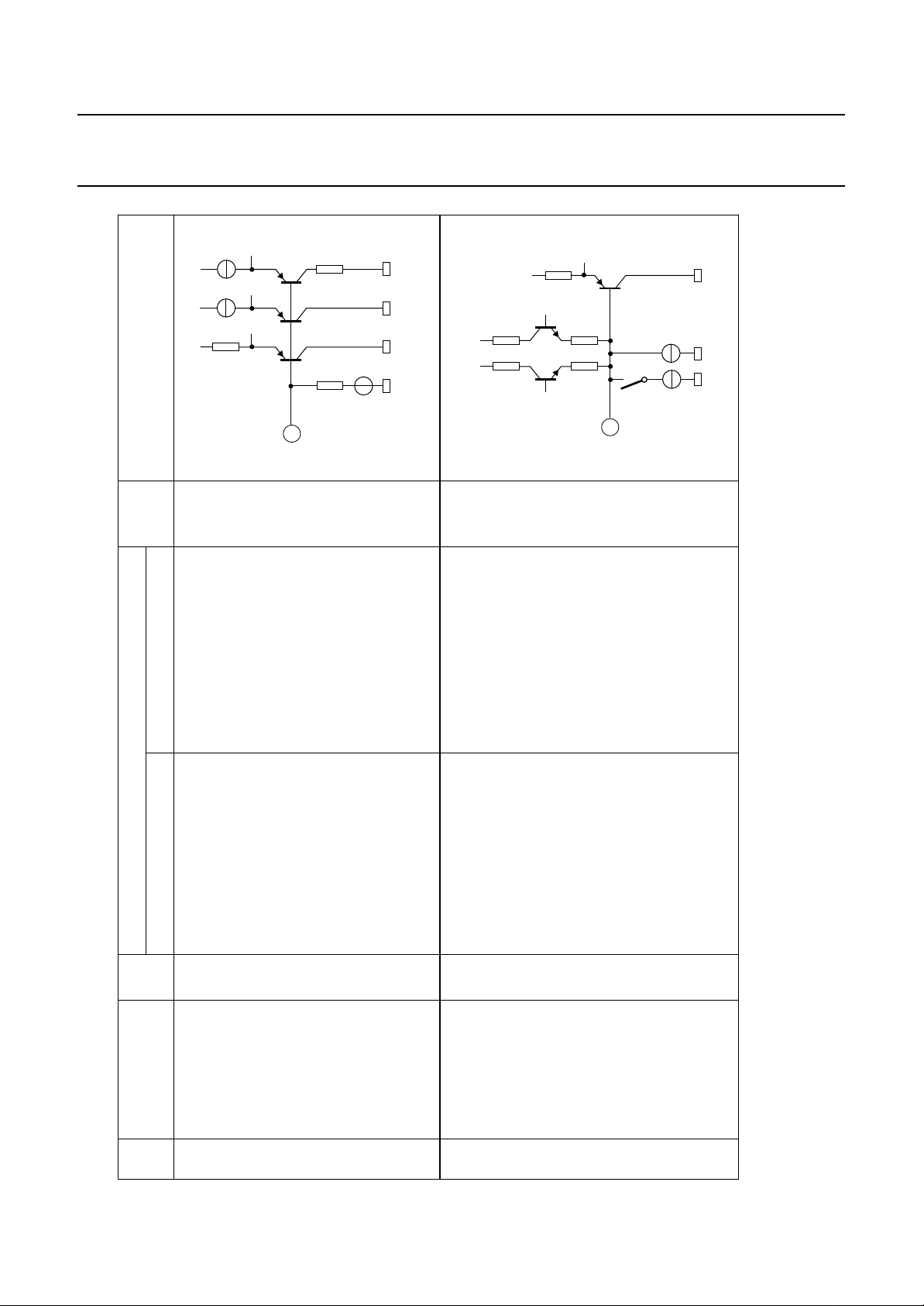
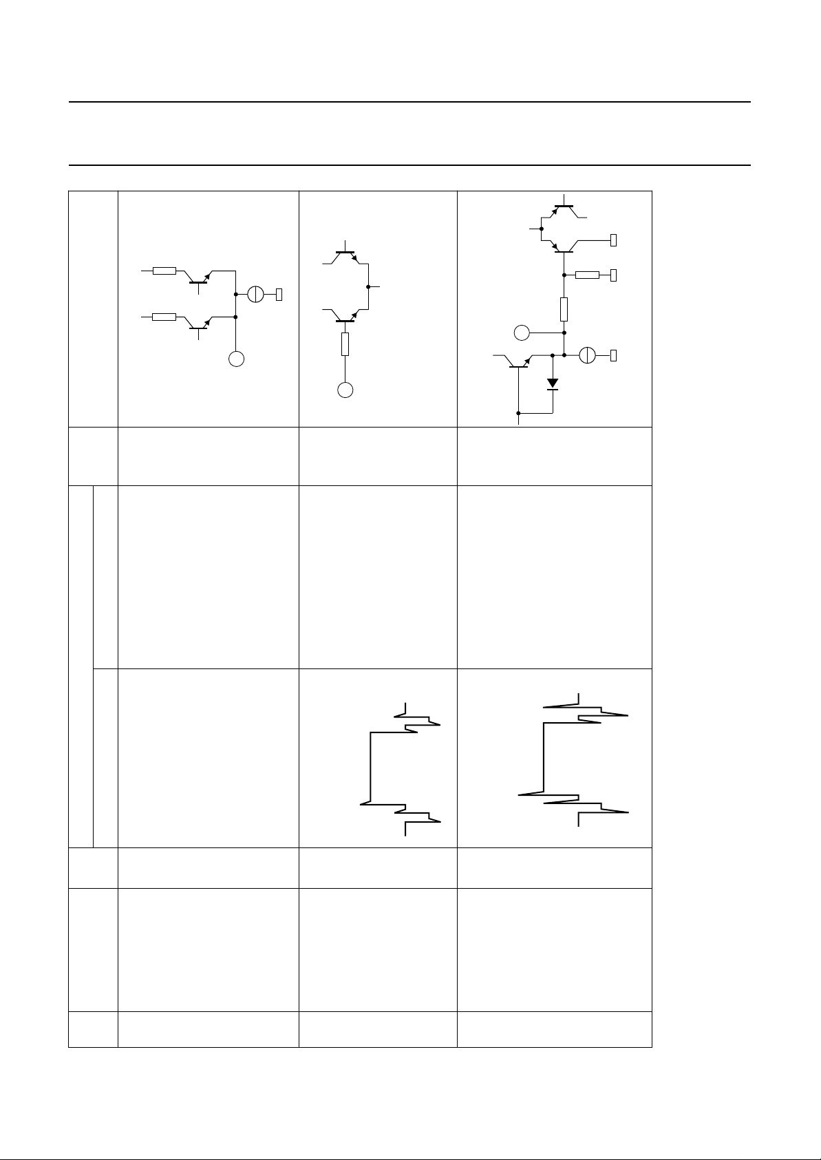
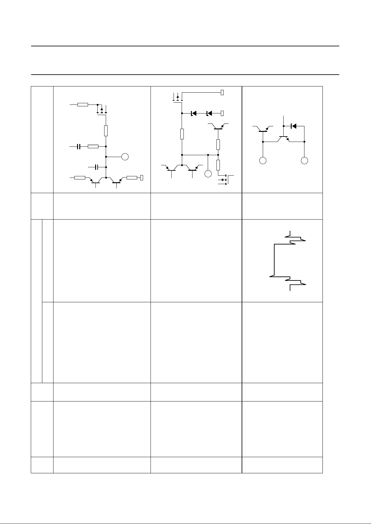
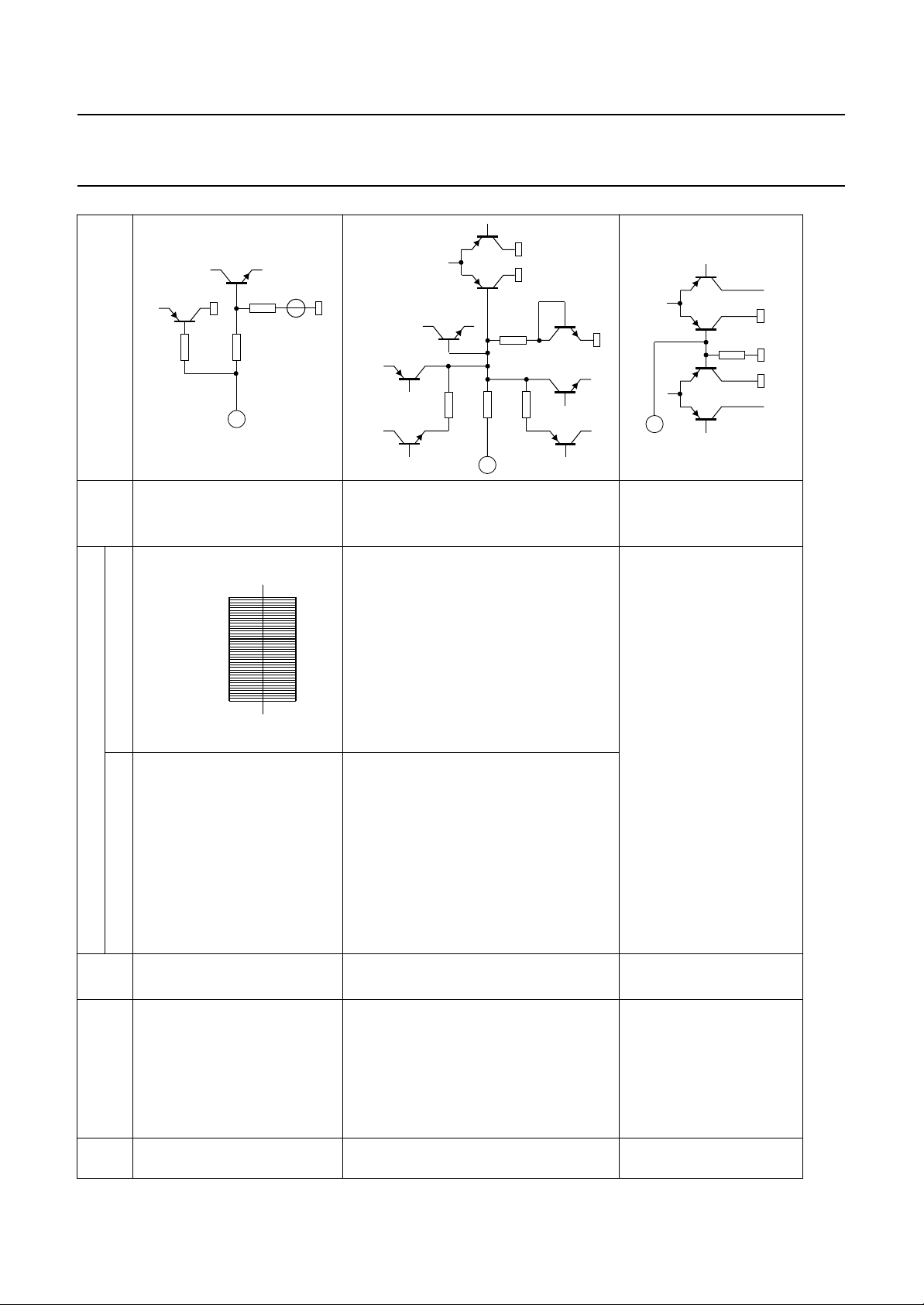
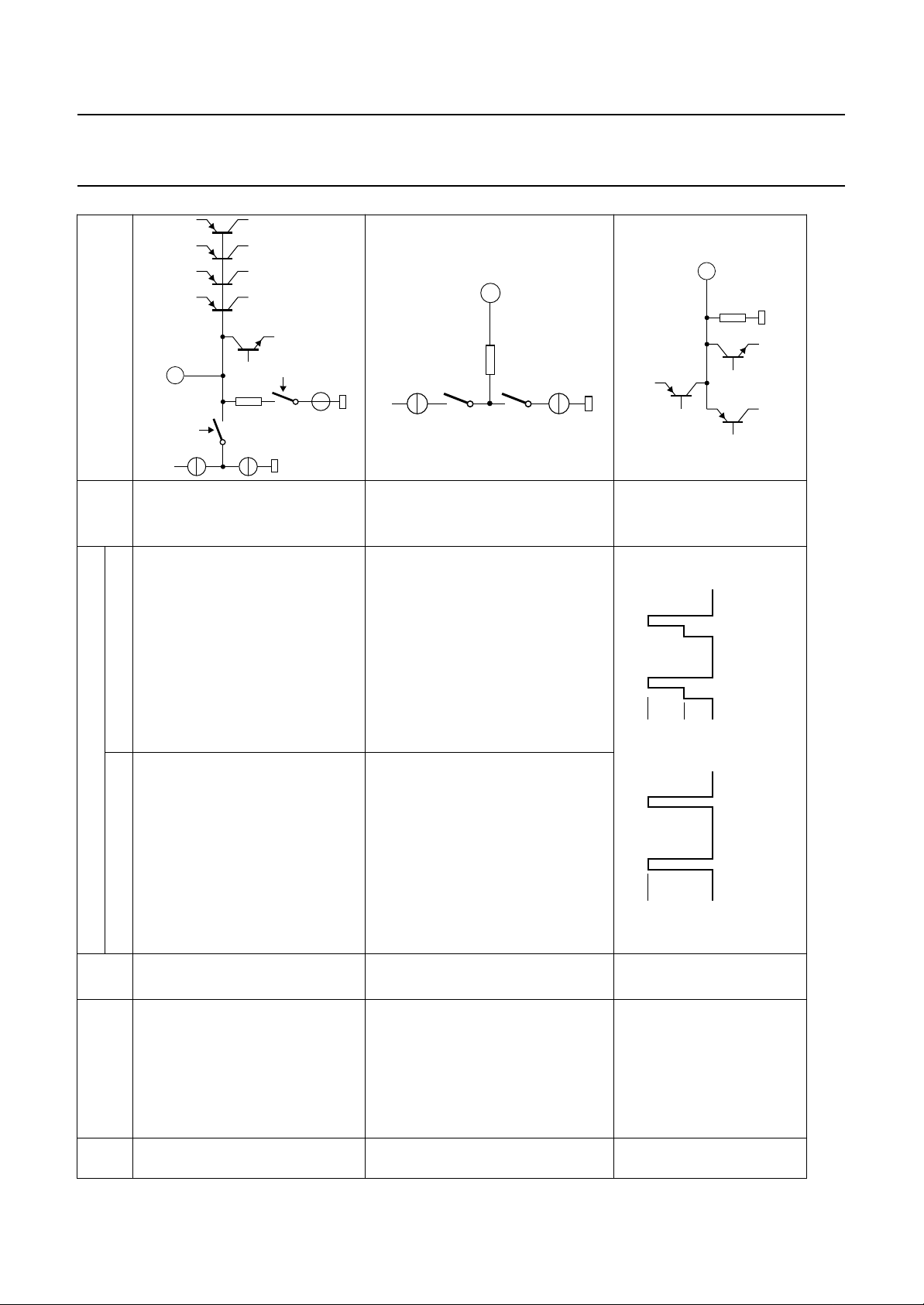
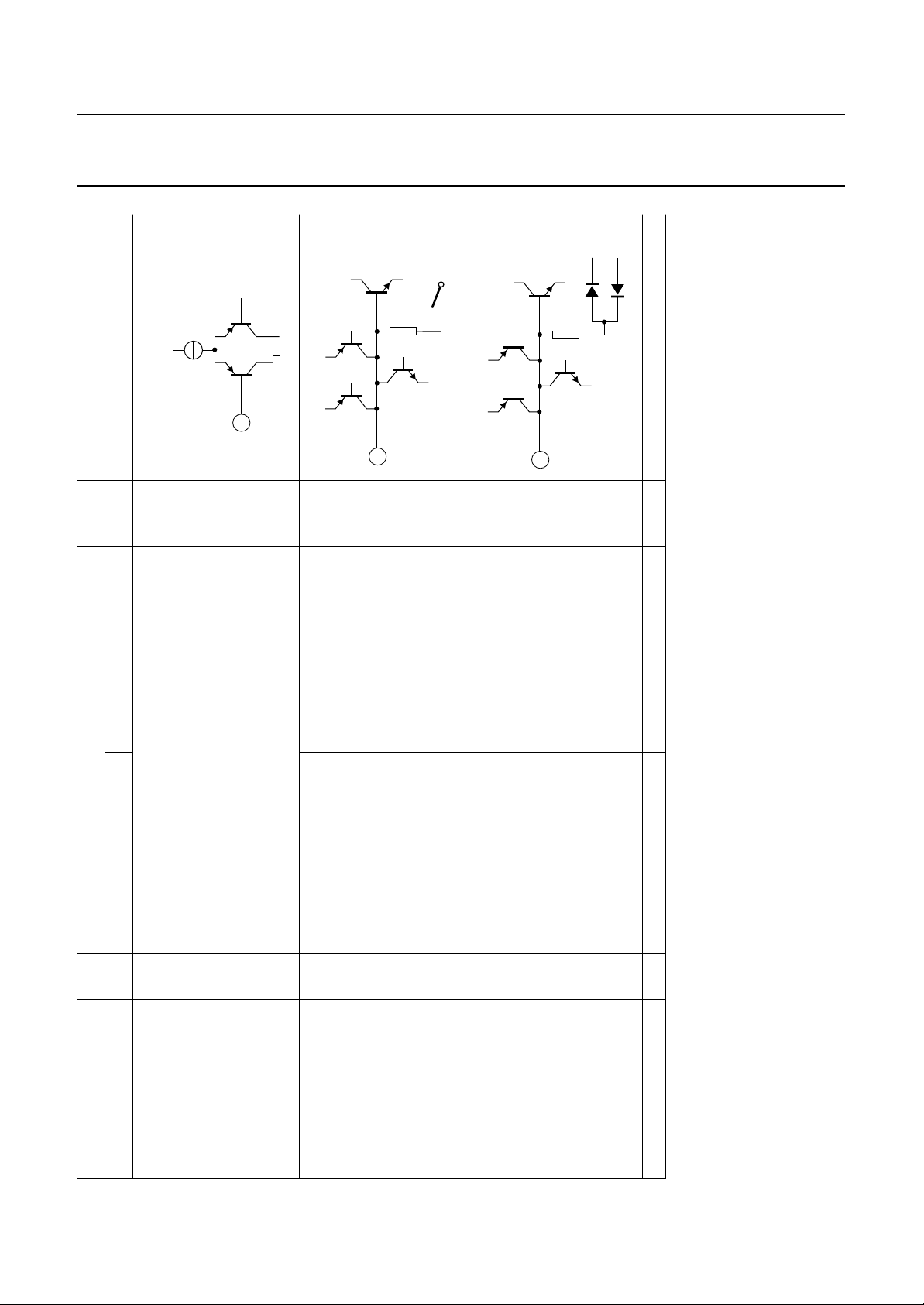
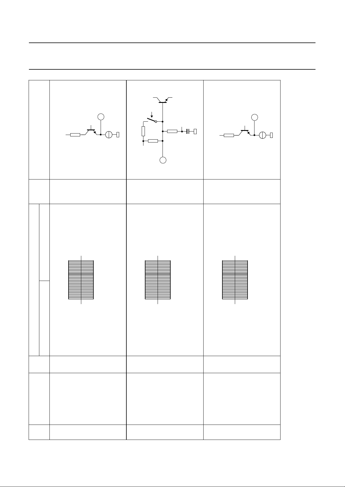
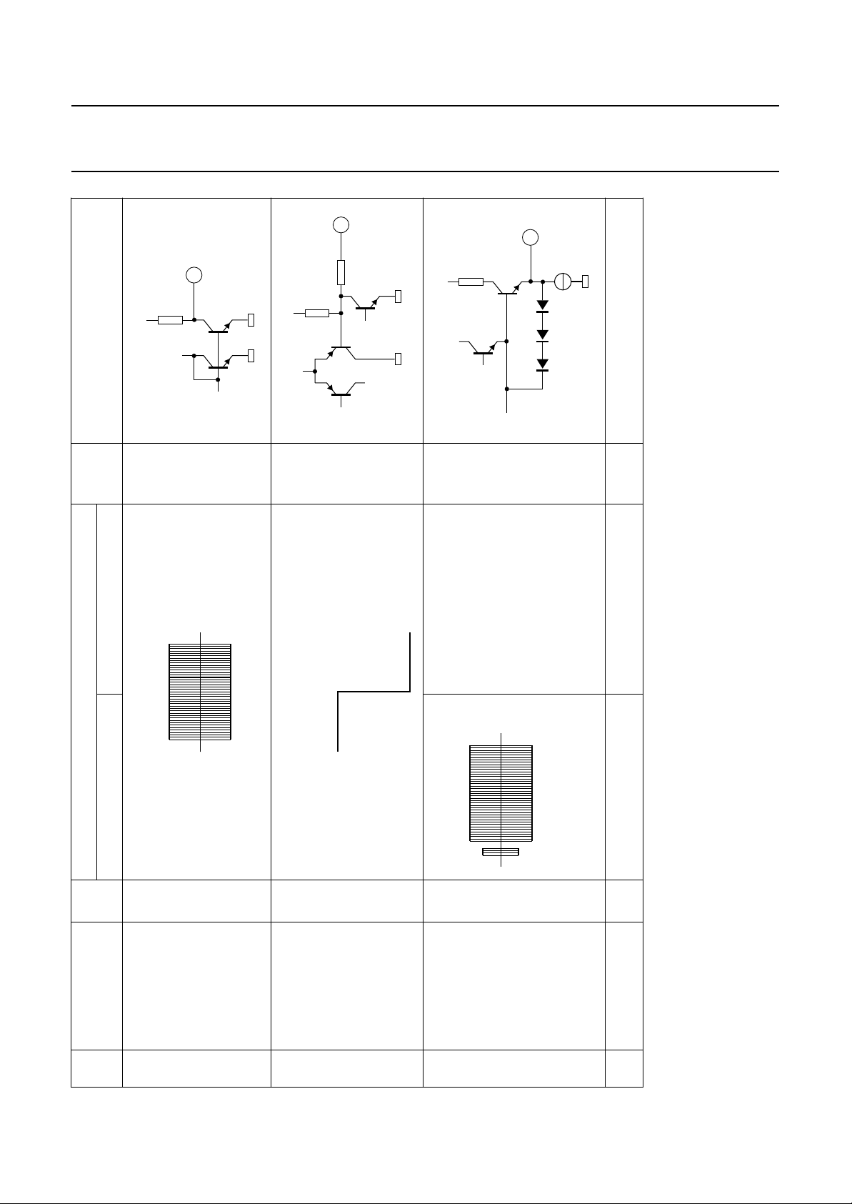
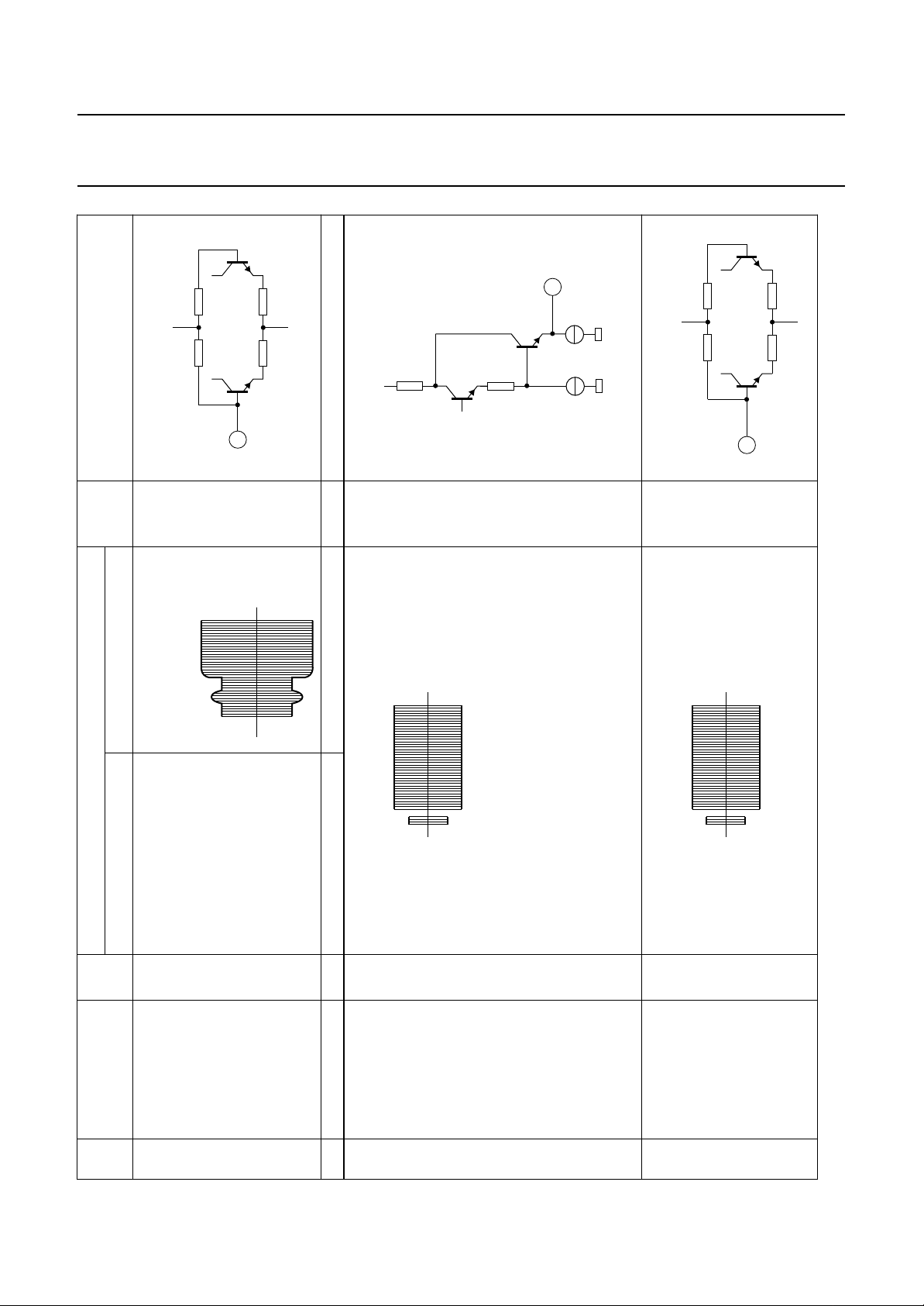
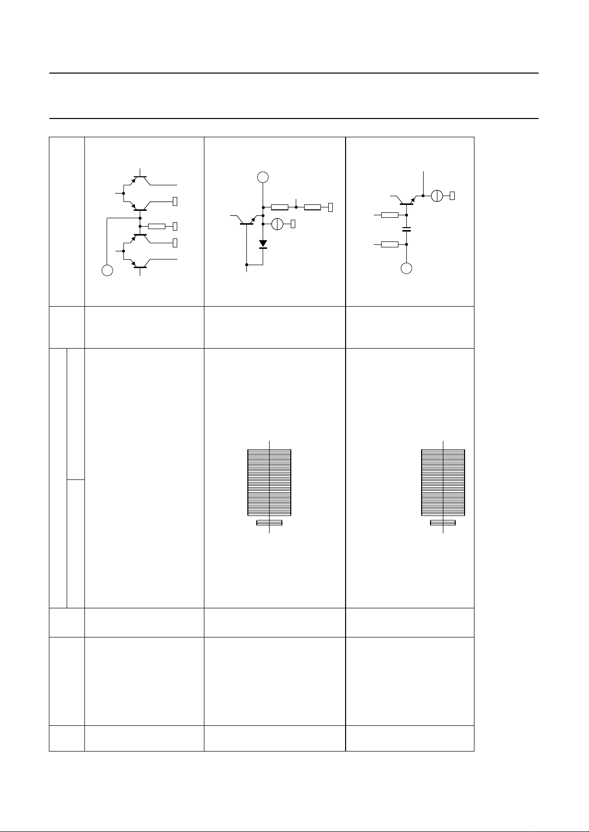
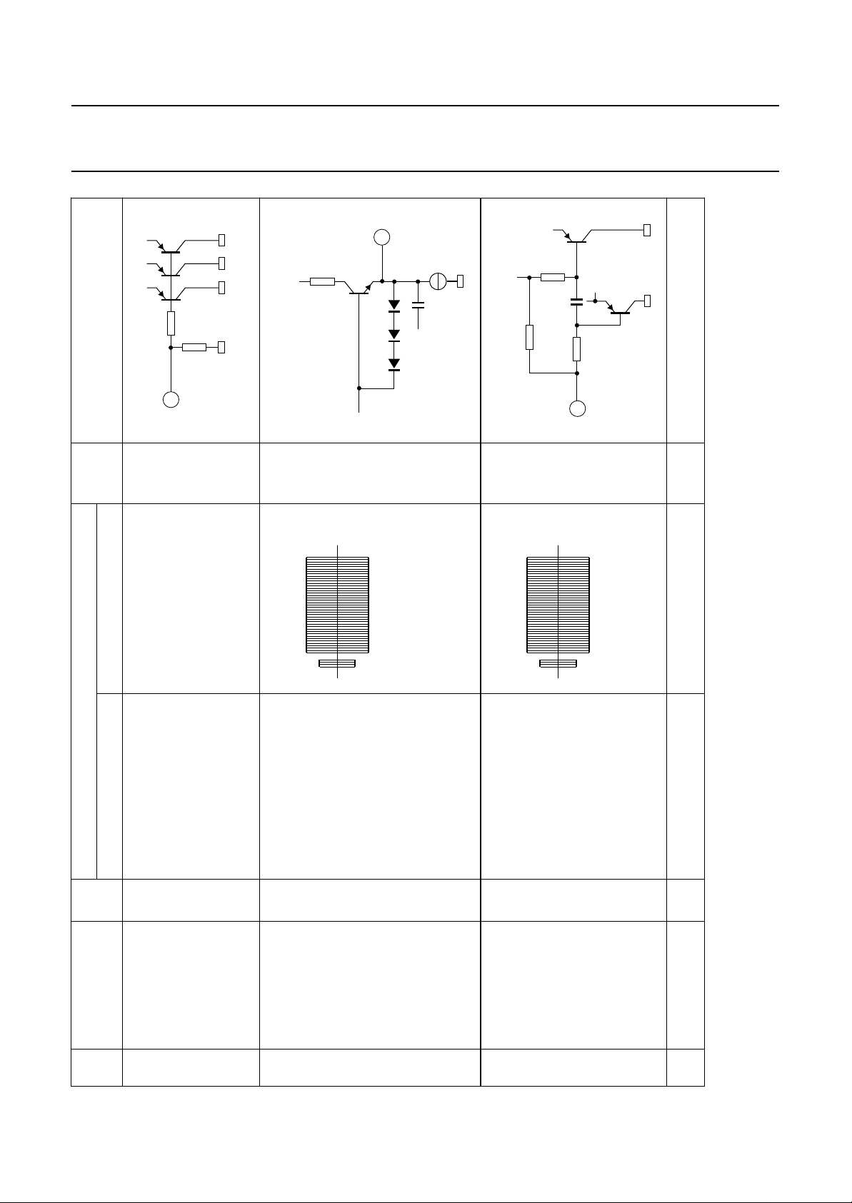
Table 13 Internal circuitry of Figs 1 and 2
NO.
control/EDIT switch
1 picture
AGC detector
2 deviation/playback
1996 Oct 14 26
Page 27
Philips Semiconductors Product specification
Y/C automatic adjustment processor
(VHS standard)
MBG106
500 µA
200 Ω
4
base
Z INTERNAL CIRCUIT
/
T
500 µA
3
MBG136
TDA9725
/1 mA
T
5
+
1 mA
MBG138
WAVEFORM
EE VV
2.1 V = COR 0 V = non-COR V
(V)
DC
PIN NAME
(DESCRIPTION)
PIN
NO.
correlation
3 test pin 2/
detector output
0 V open
1.9 V (sync)
500 mV sync-white
input of main
emphasis
4 negative feedback
0V V
MBG157
1.9 V (sync)
500 mV sync-white
output/white clip/
5 main emphasis
modulator input/
SQPB selector
MBG156
1996 Oct 14 27
Page 28
Philips Semiconductors Product specification
Y/C automatic adjustment processor
(VHS standard)
8 kΩ
MBG144
60 pF
++
+
5 kΩ
+
E
Z INTERNAL CIRCUIT
/I
T
V
10 kΩ
1.3 kΩ
6
55 pF
5 kΩ
TDA9725
5 V
5 V
10 kΩ
7
MBG143
MBG135
200 Ω
8
2 kΩ
open
collector
9
WAVEFORM
EE VV
(V)
DC
MBG159
300 mV sync-white
1.2 V 3.3 V
5 V 3.4 V (sync)
PIN NAME
(DESCRIPTION)
PIN
NO.
clamp 3
6 capacitor for
processor
0
(REC)/ envelope
detector (PB)
for f
7 storage capacitor
1996 Oct 14 28
output
8 main de-emphasis
Page 29
Philips Semiconductors Product specification
Y/C automatic adjustment processor
(VHS standard)
MBG135
CC(FM)
+
/I
+V
10
E
T
100 Ω
8
E
Z INTERNAL CIRCUIT
/I
T
V
9
TDA9725
11
100 Ω
50
kΩ
MBG107
12
50 kΩ
MBG133
WAVEFORM
EE VV
(V)
DC
300 mV sync-white
0 V 1.6 V (sync)
MBG158
5.0
3.7 V V
0.9 V (p-p) rectangle
3.5Vto5V PB
MBG154
0 V to 1.25 V REC 1.75 V to 3 V TRICK
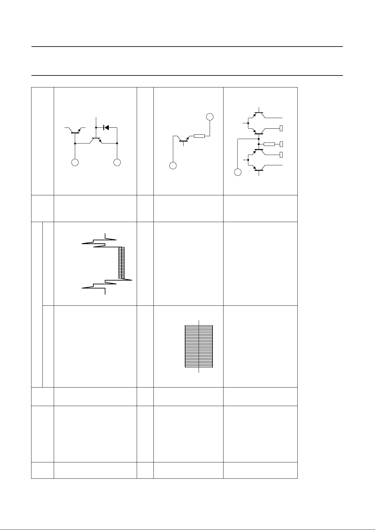
PIN NAME
(DESCRIPTION)
PIN
NO.
and peaking
9 main de-emphasis
FM parts
10 supply voltage for
11 FM output 3.2 V
1996 Oct 14 29
(PB/TRICK/REC)
12 switch
Page 30
Philips Semiconductors Product specification
Y/C automatic adjustment processor
(VHS standard)
+
+
10 kΩ
200 Ω
200 Ω
Z INTERNAL CIRCUIT
10 kΩ
13
2.2 V
MBG139
+
TDA9725
MBG142
MBG134
190 kΩ
3 kΩ
4 kΩ
200 Ω
14
15
50 kΩ
50
kΩ
WAVEFORM
EE VV
(V)
DC
200 mV (p-p) sinusoidal
(350 mV (p-p) if FM AGC off)
MBG154
3.1 V
4.3 V to 5.0 V FM AGC off
1.75Vto3.0VLP
3.5 V to 5.0 V LPC* (PAL)
3.5 V to 5.0 V EP (NTSC)
0 0 V to 1.25 V SP
PIN NAME
(DESCRIPTION)
PIN
NO.
13 PB FM input 1.6 V 2.2 V
for FM AGC
14 storage capacitor
1996 Oct 14 30
(LPC*/LP/SP) at
PAL
switch (EP/LP/SP)
at NTSC
15 switch
Page 31
Philips Semiconductors Product specification
Y/C automatic adjustment processor
(VHS standard)
MBG141
16
BGP
+
Z INTERNAL CIRCUIT
BGP
15 kΩ
1.8 V
TDA9725
18
17
MBG137
1 kΩ
+
20 kΩ
MBG132
WAVEFORM
EE VV
(V)
DC
2.8
2.1
5 V
5 V
2.2 V
0 V
0 V
MBG149
(b)
CC
(a)
(a) open circuit
(b) with 10 kΩ resistor to V
PIN NAME
(DESCRIPTION)
PIN
NO.
terminal
16 colour killer
correction output
17 frequency
1996 Oct 14 31
(HIGH active)
18 BGP output
Page 32
Philips Semiconductors Product specification
Y/C automatic adjustment processor
(VHS standard)
2.5 V
MBG131
80 kΩ
+
19
20
Z INTERNAL CIRCUIT
open
base
2.4 V
MBG130
TDA9725
2.8 V
1.4 V
1.8 kΩ
21
MBG129
WAVEFORM
EE VV
2.75Vto5VCH1
(V)
DC
2.4
PIN NAME
(DESCRIPTION)
PIN
NO.
19 rotary pulse 0 V to 2.25 V CH2
VXO
20 loop filter (REC)
1996 Oct 14 32
21 loop filter VCO 2.1
22 not connected HIGH
Page 33
Philips Semiconductors Product specification
Y/C automatic adjustment processor
(VHS standard)
+
PB
+
500 Ω
Z INTERNAL CIRCUIT
/
T
300 µA
23
MBG104
1.5 kΩ
3 V
300 µA
9 kΩ
24
1.3 kΩ
TDA9725
MBG127
25
5.2 kΩ
+
500 Ω
/
T
700 µA
MBG103
700 µA
WAVEFORM
EE VV
(V)
DC
PIN NAME
PIN
output 2.3 600 mV (p-p) V
(DESCRIPTION)
SC
NO.
23 f
MBG154
3.0 250 mV (p-p) 9 kΩ/
crystal
24 VXO input from
MBG154
MBG154
3.3 230 mV (p-p) V
crystal
25 VXO output to
1996 Oct 14 33
Page 34
Philips Semiconductors Product specification
Y/C automatic adjustment processor
(VHS standard)
27
MBG110
26
8.0 kΩ
7.5 kΩ
Z INTERNAL CIRCUIT
MBG109
2 kΩ
+
30
kΩ
2.5 V
TDA9725
500 Ω
/
T
0.8 mA
V
28
0.8 mA
MBG111
WAVEFORM
EE VV
(V)
DC
PIN NAME
output 4.9 550 mV (p-p)
SC
(DESCRIPTION)
MBG154
5 V
PB + REC
PB: forced 0 V: NTSC4.43 mode
output
H/2
(coupled to burst
sequence)
NAP/NTSC4.43
switch
0 V
MBG148
2.4 660 mV (p-p) 2.4 V normal
0 V colour off
output to tape
MBG153
5.0
chrominance
PIN
NO.
26 2f
27 f
1996 Oct 14 34
28 chrominance
29 supply voltage
Page 35
Philips Semiconductors Product specification
Y/C automatic adjustment processor
(VHS standard)
MBG115
2.2 V
10 kΩ 10 kΩ
+
1 kΩ
30
Z INTERNAL CIRCUIT
10 kΩ
/
T
400 µA
TDA9725
MBG124
32
MBG125
400 µA
8 kΩ
1.9 V
2.7 kΩ 2.7 kΩ
33
WAVEFORM
EE VV
(V)
DC
and FM
2.2 chrominance 110 mV (p-p)
MBG155
MBG153
MBG153
1.9 440 mV (p-p) 2.7 kΩ
PIN NAME
(DESCRIPTION)
PIN
NO.
input from tape
30 PB chrominance
31 ground 0
32 ACC output 2.25 440 mV (p-p) V
1996 Oct 14 35
input
33 balanced mixer
Page 36
Philips Semiconductors Product specification
Y/C automatic adjustment processor
(VHS standard)
35
1 mA
34
Z INTERNAL CIRCUIT
50 kΩ
MBG123
/1 mA
T
V
+
50
kΩ
TDA9725
11 µA
710 Ω
120 Ω
+
10 kΩ
4.0 V
MBG116
80 kΩ/
9kΩ
80 kΩ
36
MBG101
WAVEFORM
EE VV
1.75 V to 3.0 V NTSC
(V)
DC
0 0Vto1.25VPAL
PIN NAME
(DESCRIPTION)
SECAM/NTSC/PAL
3.5 V to 5.0 V SECAM
NTSC or CCD: 380 mV (p-p)
MBG153
4.0 V: glass comb
<1.5 V: CCD comb
4.0 120 mV (p-p)
from comb filter
MBG153
PIN
NO.
34 switch
35 comb driver output 2.5 PAL and glass: 675 mV (p-p)
1996 Oct 14 36
36 chrominance input
Page 37
Philips Semiconductors Product specification
Y/C automatic adjustment processor
(VHS standard)
38
4 kΩ
50 kΩ
37
Z INTERNAL CIRCUIT
MBG114
/
T
200 Ω
+
600 µA
TDA9725
600 µA
MBG102
2.0 V
100 kΩ
20 kΩ
45 pF
200 Ω
39
MBG122
WAVEFORM
EE VV
(V)
DC
MBG153
MBG153
>3.4 V: AGCKP1 325 mV (p-p) 20 kΩ
1.6 325 mV (p-p) V
1.6
(2.0)
5.0
PIN NAME
(DESCRIPTION)
PIN
NO.
37 test pin 1 0 50 kΩ
output
38 PB chrominance
1996 Oct 14 37
input
39 PB chrominance
luminance
40 supply voltage
Page 38
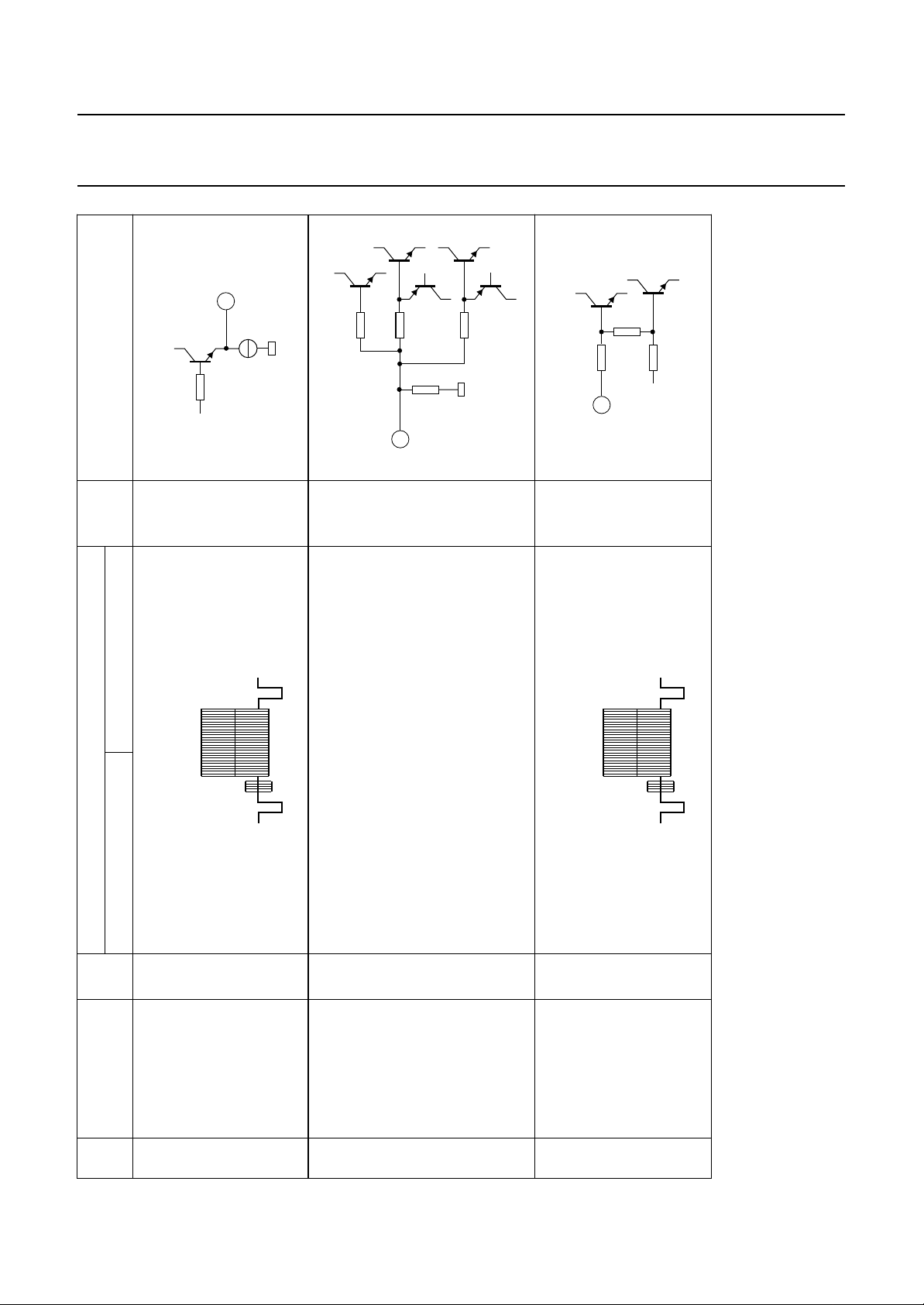
Philips Semiconductors Product specification
Y/C automatic adjustment processor
(VHS standard)
41
+
5 kΩ
Z INTERNAL CIRCUIT
/1 mA
T
V
1.0 mA
MBG113
2 kΩ
50 kΩ
50 kΩ
42
50 kΩ
TDA9725
+
50 kΩ
MBG119
+
3.5 kΩ
20 kΩ
43
11.5 kΩ
2.75 V
MBG120
WAVEFORM
EE VV
sync-white: 2.14 V (p-p)
chrominance: 1.2 V (p-p)
(V)
DC
sync
PIN NAME
(DESCRIPTION)
MBG152
0.0 0 V to 1.0 V through
1.5 V to 2.25 V white
2.75 V to 3.5 V black
4.0 V to 5.0 V sync
(artificial sync/
black/white/
through)
MBG152
chrominance: 660 mV (p-p)
PIN
NO.
41 video output 1.05
42 character insert
1996 Oct 14 38
43 video input 2.75 sync-white: 1.0 V (p-p)
Page 39
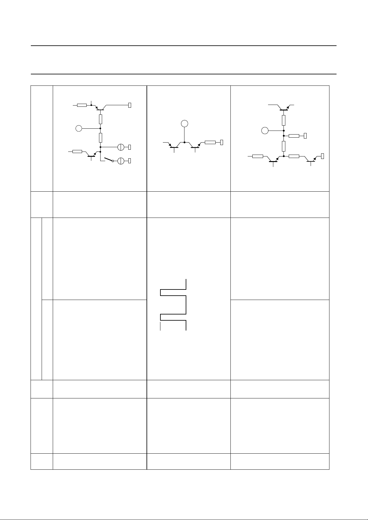
Philips Semiconductors Product specification
Y/C automatic adjustment processor
(VHS standard)
+
40 kΩ
44
+
2.4 kΩ
+
E
Z INTERNAL CIRCUIT
/I
T
100 Ω
1 kΩ
125 Ω
MBG121
2.5 µA60 µA
+
TDA9725
+
MBG117
45
MBG112
+
/I
+
E
T
500 Ω
200 Ω
46
500 Ω 500 Ω
200 Ω
200 kΩ 220 kΩ
WAVEFORM
EE VV
(V)
DC
PIN NAME
(DESCRIPTION)
5 V
output
MBG147
0 V
3.1 V
detector
PIN
NO.
44 AGC detector 2.5 V
45 sync separator
1996 Oct 14 39
46 sync separator
Page 40
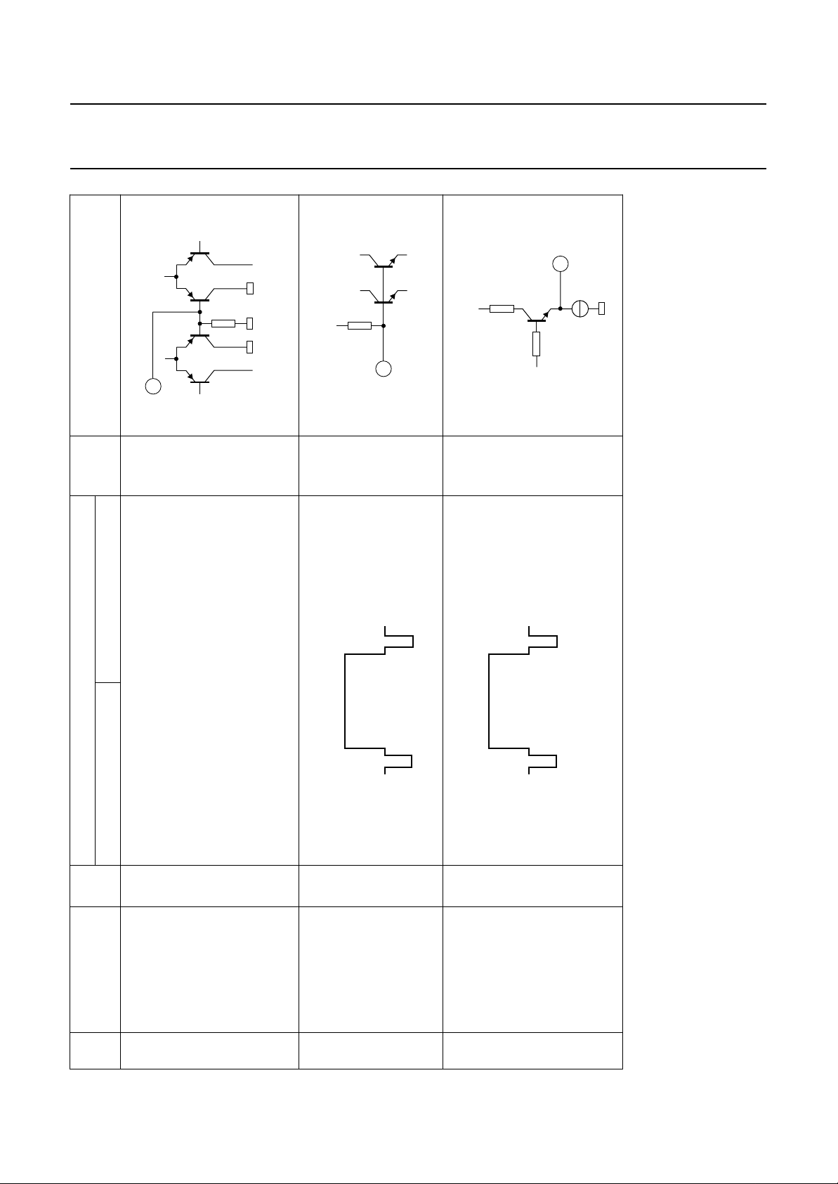
Philips Semiconductors Product specification
Y/C automatic adjustment processor
(VHS standard)
MBG118
50
kΩ
1.9 V
40 kΩ
48
47
Z INTERNAL CIRCUIT
50 kΩ
MBG100
TDA9725
49
500 Ω
+
5 kΩ
/
T
230 µA
230 µA
MBG105
WAVEFORM
EE VV
1.75 V to 3.0 V YNR1
(V)
DC
PIN NAME
(DESCRIPTION)
MBG146
3.5 V to 5.0 V YNR off
1.9 283 mV (p-p) 40 kΩ
1H CCD
420 mV (p-p) V
1.4
sync
1H CCD
MBG146
PIN
NO.
47 YNR switch 0 0 V to 1.25 V YNR2
48 video input from
1996 Oct 14 40
49 video output to
Page 41
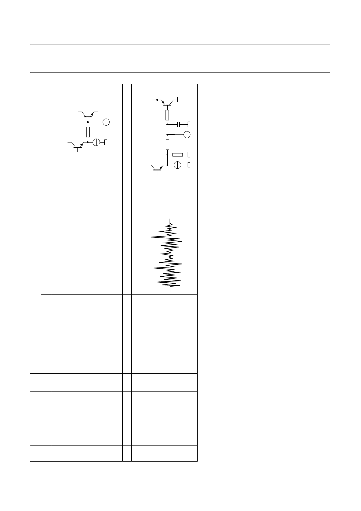
Philips Semiconductors Product specification
Y/C automatic adjustment processor
(VHS standard)
260 Ω
1 kΩ
+
+
20 kΩ
Z INTERNAL CIRCUIT
50
95 µA
MBG108
230
15 pF
50 kΩ
µA
MBG128
52
MBG151
TDA9725
WAVEFORM
EE VV
(V)
DC
2.0
1.2 noise 1 kΩ
PIN NAME
(DESCRIPTION)
PIN
NO.
for CCD level AGC
50 storage capacitor
noise canceller
51 ground luminance 0
52 low-pass filter for
1996 Oct 14 41
Page 42
Philips Semiconductors Product specification
Y/C automatic adjustment processor
(VHS standard)
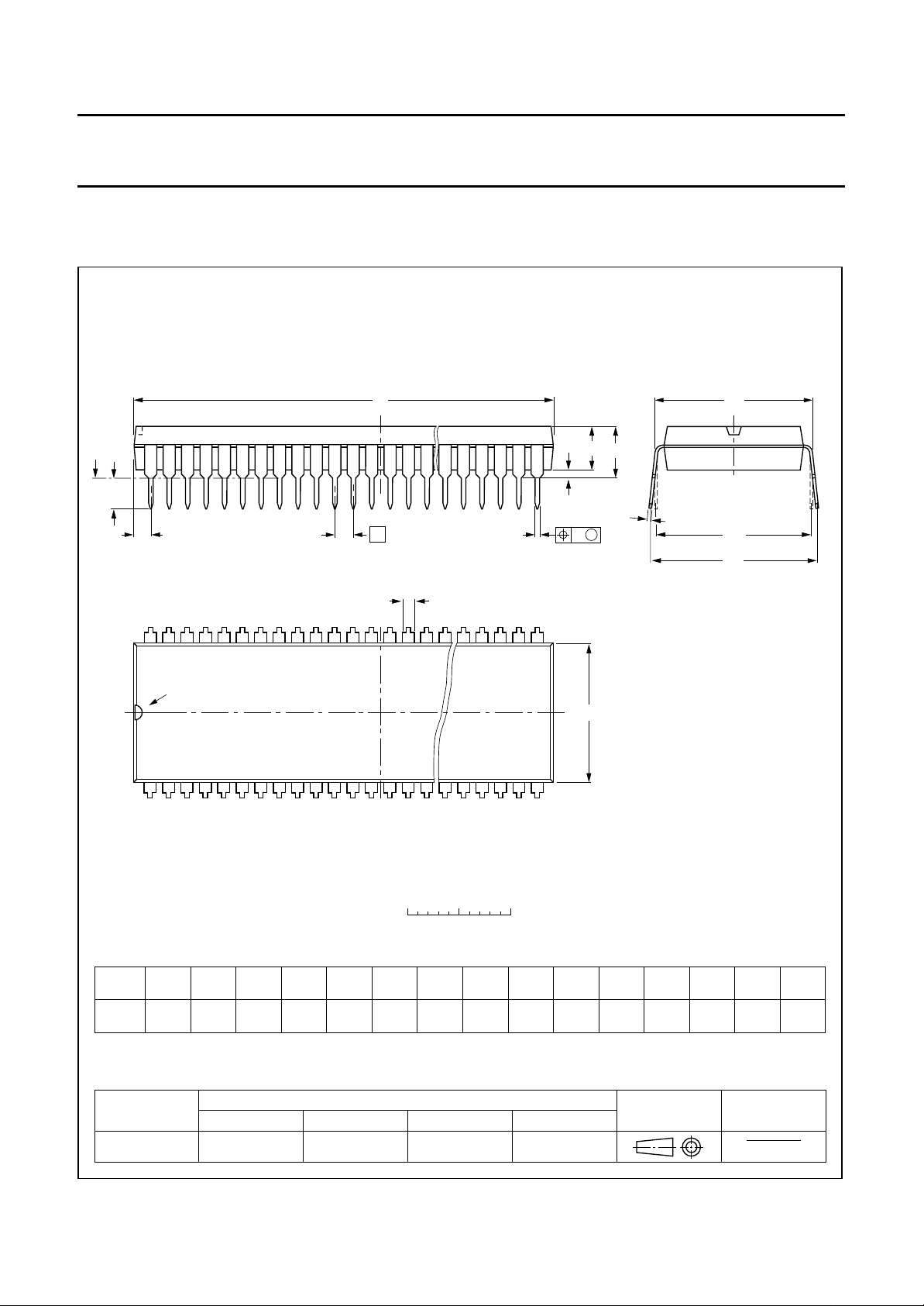
PACKAGE OUTLINE
SDIP52: plastic shrink dual in-line package; 52 leads (600 mil)
D
seating plane
L
Z
e
TDA9725
SOT247-1
M
E
A
2
A
A
1
w M
b
1
c
(e )
M
1
H
52
pin 1 index
1
DIMENSIONS (mm are the original dimensions)
A
A
A
UNIT b
mm
max.
5.08 0.51 4.0
12
min.
max.
b
1.3
0.8
0.53
0.40
b
27
E
26
0 5 10 mm
scale
cEe M
1
0.32
0.23
(1) (1)
D
47.9
47.1
14.0
13.7
1
L
M
E
3.2
15.80
2.8
15.24
17.15
15.90
e
w
H
0.181.778 15.24
Z
max.
1.73
(1)
Note
1. Plastic or metal protrusions of 0.25 mm maximum per side are not included.
OUTLINE
VERSION
SOT247-1
IEC JEDEC EIAJ
REFERENCES
1996 Oct 14 42
EUROPEAN
PROJECTION
ISSUE DATE
90-01-22
95-03-11
Page 43
Philips Semiconductors Product specification
Y/C automatic adjustment processor
(VHS standard)
SOLDERING
Introduction
There is no soldering method that is ideal for all IC
packages. Wave soldering is often preferred when
through-hole and surface mounted components are mixed
on one printed-circuit board. However, wave soldering is
not always suitable for surface mounted ICs, or for
printed-circuits with high population densities. In these
situations reflow soldering is often used.
This text gives a very brief insight to a complex technology.
A more in-depth account of soldering ICs can be found in
our
“IC Package Databook”
Soldering by dipping or by wave
The maximum permissible temperature of the solder is
260 °C; solder at this temperature must not be in contact
with the joint for more than 5 seconds. The total contact
time of successive solder waves must not exceed
5 seconds.
(order code 9398 652 90011).
TDA9725
The device may be mounted up to the seating plane, but
the temperature of the plastic body must not exceed the
specified storage maximum (T
board has been pre-heated, forced cooling may be
necessary immediately after soldering to keep the
temperature within the permissible limit.
Repairing soldered joints
Apply a low voltage soldering iron (less than 24 V) to the
lead(s) of the package, below the seating plane or not
more than 2 mm above it. If the temperature of the
soldering iron bit is less than 300 °C it may remain in
contact for up to 10 seconds. If the bit temperature is
between 300 and 400 °C, contact may be up to 5 seconds.
). If the printed-circuit
stg max
DEFINITIONS
Data sheet status
Objective specification This data sheet contains target or goal specifications for product development.
Preliminary specification This data sheet contains preliminary data; supplementary data may be published later.
Product specification This data sheet contains final product specifications.
Limiting values
Limiting values given are in accordance with the Absolute Maximum Rating System (IEC 134). Stress above one or
more of the limiting values may cause permanent damage to the device. These are stress ratings only and operation
of the device at these or at any other conditions above those given in the Characteristics sections of the specification
is not implied. Exposure to limiting values for extended periods may affect device reliability.
Application information
Where application information is given, it is advisory and does not form part of the specification.
LIFE SUPPORT APPLICATIONS
These products are not designed for use in life support appliances, devices, or systems where malfunction of these
products can reasonably be expected to result in personal injury. Philips customers using or selling these products for
use in such applications do so at their own risk and agree to fully indemnify Philips for any damages resulting from such
improper use or sale.
1996 Oct 14 43
Page 44

Philips Semiconductors – a worldwide company
Argentina: see South America
Australia: 34 Waterloo Road, NORTH RYDE, NSW 2113,
Tel. +61 2 9805 4455, Fax. +61 29805 4466
Austria: Computerstr. 6, A-1101 WIEN, P.O. Box 213,
Tel. +43 1 60 101, Fax. +43 1 60 101 1210
Belarus: Hotel Minsk Business Center, Bld. 3, r. 1211, Volodarski Str.6,
220050 MINSK, Tel. +375 172 200 733, Fax. +375 172 200773
Belgium: see The Netherlands
Brazil: see South America
Bulgaria: Philips Bulgaria Ltd., Energoproject, 15th floor,
51 James Bourchier Blvd., 1407 SOFIA,
Tel. +359 2 689 211, Fax. +359 2689 102
Canada: PHILIPS SEMICONDUCTORS/COMPONENTS,
Tel. +1 800 234 7381
China/Hong Kong: 501 Hong Kong Industrial Technology Centre,
72 Tat Chee Avenue, Kowloon Tong, HONG KONG,
Tel. +852 2319 7888, Fax. +8522319 7700
Colombia: see South America
Czech Republic: see Austria
Denmark: Prags Boulevard 80, PB 1919, DK-2300 COPENHAGEN S,
Tel. +45 32 88 2636, Fax. +45 31 57 1949
Finland: Sinikalliontie 3, FIN-02630 ESPOO,
Tel. +358 9 615800, Fax. +358 9 61580/xxx
France: 4 Rue du Port-aux-Vins, BP317, 92156 SURESNES Cedex,
Tel. +33 1 40 99 6161, Fax. +33 1 4099 6427
Germany: Hammerbrookstraße 69, D-20097 HAMBURG,
Tel. +49 40 23 53 60, Fax. +4940 23536 300
Greece: No. 15, 25th March Street, GR 17778 TAVROS/ATHENS,
Tel. +30 1 4894 339/239, Fax. +30 14814 240
Hungary: see Austria
India: Philips INDIA Ltd, Shivsagar Estate, A Block, Dr. Annie Besant Rd.
Worli, MUMBAI 400 018, Tel. +91 22 4938541, Fax.+91 224938 722
Indonesia: see Singapore
Ireland: Newstead, Clonskeagh, DUBLIN 14,
Tel. +353 1 7640 000, Fax.+353 17640 200
Israel: RAPAC Electronics, 7 Kehilat Saloniki St, TEL AVIV 61180,
Tel. +972 3 645 0444, Fax.+972 3649 1007
Italy: PHILIPS SEMICONDUCTORS, Piazza IV Novembre 3,
20124 MILANO, Tel. +39 2 6752 2531, Fax. +392 67522557
Japan: Philips Bldg 13-37, Kohnan 2-chome, Minato-ku, TOKYO 108,
Tel. +81 3 3740 5130, Fax. +81 33740 5077
Korea: Philips House, 260-199 Itaewon-dong, Yongsan-ku, SEOUL,
Tel. +82 2 709 1412, Fax. +82 2 709 1415
Malaysia: No. 76 Jalan Universiti, 46200 PETALING JAYA, SELANGOR,
Tel. +60 3 750 5214, Fax. +603 7574880
Mexico: 5900 Gateway East, Suite 200, EL PASO, TEXAS 79905,
Tel. +9-5 800 234 7381
Middle East: see Italy
Netherlands: Postbus 90050, 5600 PB EINDHOVEN, Bldg. VB,
Tel. +31 40 27 82785, Fax.+31 4027 88399
New Zealand: 2 Wagener Place, C.P.O. Box 1041, AUCKLAND,
Tel. +64 9 849 4160, Fax. +64 9 849 7811
Norway: Box 1, Manglerud 0612, OSLO,
Tel. +47 22 74 8000, Fax. +47 22 74 8341
Philippines: Philips Semiconductors Philippines Inc.,
106 Valero St. Salcedo Village, P.O. Box2108 MCC,MAKATI,
Metro MANILA, Tel. +63 2 816 6380, Fax. +632 817 3474
Poland: Ul. Lukiska 10, PL 04-123 WARSZAWA,
Tel. +48 22 612 2831, Fax.+48 22612 2327
Portugal: see Spain
Romania: see Italy
Russia: Philips Russia, Ul. Usatcheva 35A, 119048 MOSCOW,
Tel. +7 095 247 9145, Fax.+7 095247 9144
Singapore: Lorong 1, Toa Payoh, SINGAPORE 1231,
Tel. +65 350 2538, Fax. +65 251 6500
Slovakia: see Austria
Slovenia: see Italy
South Africa: S.A. PHILIPS Pty Ltd., 195-215 Main Road Martindale,
2092 JOHANNESBURG, P.O. Box 7430 Johannesburg 2000,
Tel. +27 11 470 5911, Fax.+27 11470 5494
South America: Rua do Rocio 220, 5th floor, Suite 51,
04552-903 São Paulo, SÃO PAULO - SP, Brazil,
Tel. +55 11 821 2333, Fax.+55 11829 1849
Spain: Balmes 22, 08007 BARCELONA,
Tel. +34 3 301 6312, Fax. +34 3 301 4107
Sweden: Kottbygatan 7, Akalla, S-16485 STOCKHOLM,
Tel. +46 8 632 2000, Fax. +46 8 632 2745
Switzerland: Allmendstrasse 140, CH-8027 ZÜRICH,
Tel. +41 1 488 2686, Fax. +41 1 481 7730
Taiwan: PHILIPS TAIWAN Ltd., 23-30F, 66,
Chung Hsiao West Road, Sec. 1, P.O. Box 22978,
TAIPEI 100, Tel. +886 2 382 4443, Fax.+886 2382 4444
Thailand: PHILIPS ELECTRONICS (THAILAND) Ltd.,
209/2 Sanpavuth-Bangna Road Prakanong, BANGKOK 10260,
Tel. +66 2 745 4090, Fax. +66 2 398 0793
Turkey: Talatpasa Cad. No. 5, 80640 GÜLTEPE/ISTANBUL,
Tel. +90 212 279 2770, Fax. +90 212 282 6707
Ukraine: PHILIPS UKRAINE, 4 Patrice Lumumba str., Building B, Floor 7,
252042 KIEV, Tel. +380 44 264 2776, Fax. +38044 2680461
United Kingdom: Philips Semiconductors Ltd., 276 Bath Road, Hayes,
MIDDLESEX UB3 5BX, Tel. +44 181 730 5000, Fax.+44 181754 8421
United States: 811 East Arques Avenue, SUNNYVALE, CA 94088-3409,
Tel. +1 800 234 7381
Uruguay: see South America
Vietnam: see Singapore
Yugoslavia: PHILIPS, Trg N. Pasica 5/v, 11000 BEOGRAD,
Tel. +381 11 625 344, Fax.+38111 635777
For all other countries apply to: Philips Semiconductors, Marketing & Sales Communications,
Building BE-p, P.O. Box 218, 5600 MD EINDHOVEN, TheNetherlands, Fax.+31 4027 24825
© Philips Electronics N.V. 1996 SCA52
All rights are reserved. Reproduction in whole or in part is prohibited without the prior written consent of the copyright owner.
The information presented in this document does not form part of any quotation or contract, is believed to be accurate and reliable and may be changed
without notice. No liability will be accepted by the publisher for any consequence of its use. Publication thereof does not convey nor imply any license
under patent- or other industrial or intellectual property rights.
Internet: http://www.semiconductors.philips.com
Printed in The Netherlands 537021/50/02/pp44 Date of release: 1996 Oct 14 Document order number: 9397 750 01024
 Loading...