

Page 1

INTEGRATED CIRCUITS
DATA SH EET
TDA9178
YUV one chip picture improvement
based on luminance vector-, colour
vector- and spectral processor
Preliminary specification
File under Integrated Circuits, IC02
1999 Sep 24
Page 2

Philips Semiconductors Preliminary specification
YUV one chip picture improvement based on luminance
vector-, colour vector- and spectral processor
FEATURES
• Picture content dependent non-linear Y, U and V
processing by luminance histogram analysis
• Variable gamma control
• Adaptive black and white stretch control
• Skin tone correction
• Green enhancement
• Blue stretch
• Luminance Transient Improvement (LTI)
• Smart peaking for detail enhancement
• Colour Transient Improvement (CTI)
• SCAn VElocity Modulation (SCAVEM) output
• Line Width Control (LWC)
• Video Dependent Coring (VDC)
• Colour Dependent Sharpness (CDS)
• Noise measurement
• Feature Mode (FM) detector
• Cue Flash (CF) detector
• Three additional pins for access to 6-bit ADC and
I2C-bus
• Adjustable chrominance delay
• TV standard independent
• I2C-bus controlled
• 1fH and 2f
• DEmonstration MOde (DEMO).
GENERAL DESCRIPTION
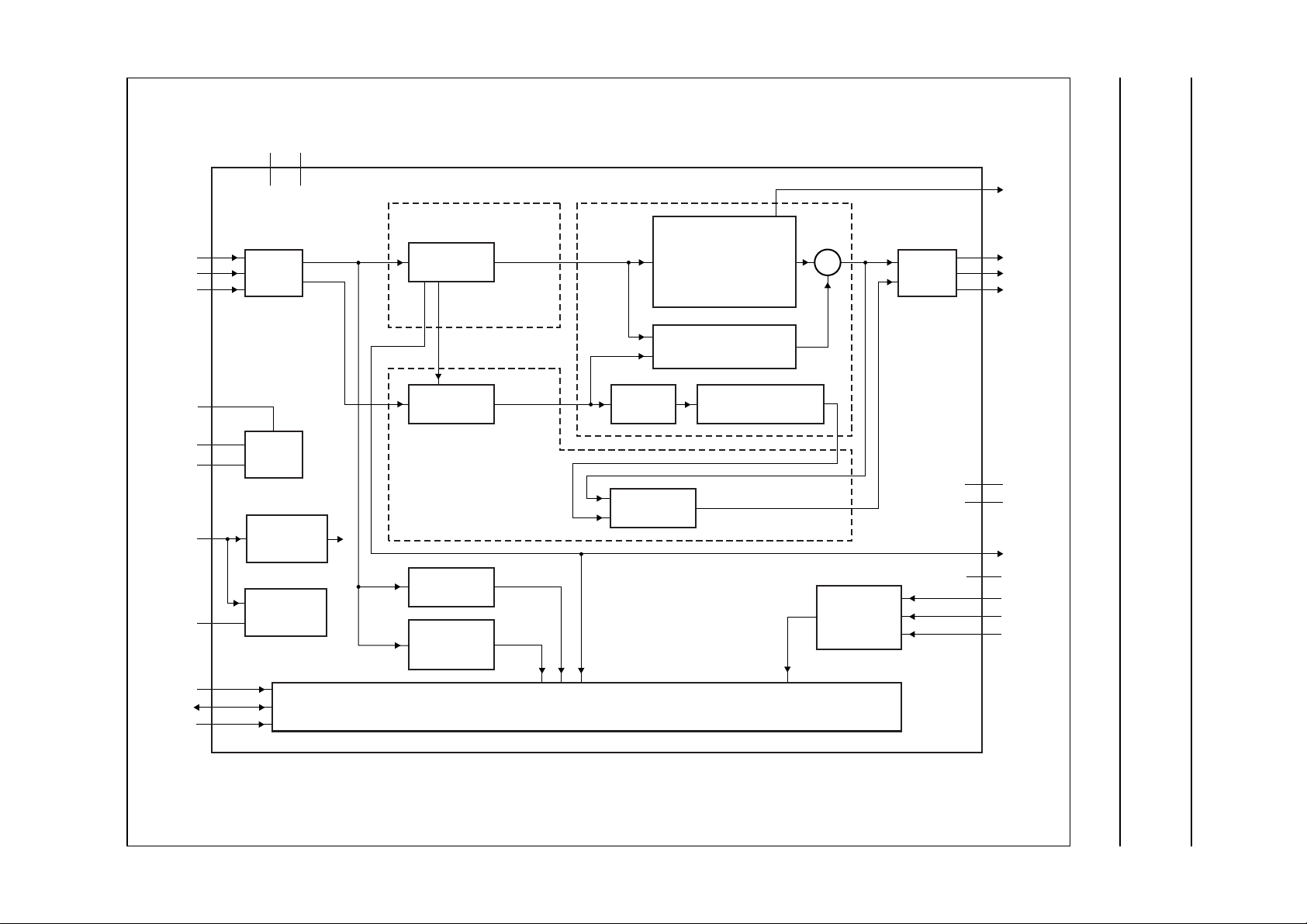
The TDA9178 is a transparent analog video processor
with YUV input and output interfaces. It offers three main
functions: luminance vector processing, colour vector
processing and spectral processing. Beside these three
main functions, there are some additional functions.
In the luminancevector processor, the luminance transfer
function is controlled in a non-linear way by the
distribution, in 5 discrete histogram sections, of the
luminance values measured in a picture. As a result, the
contrast ratio of the most important parts of the scene will
be improved. Black restoration is available in the event of
a set-up in the luminance signal.
A variable gamma function, after the histogram
conversion,offersthepossibilitiesofalternativebrightness
control or factory adjustment of the picture tube.
H
The adaptive black stretch function of the TDA9178 offers
the possibility of having a larger ‘weight’ for the black parts
of the video signal; the white stretch function offers an
additional overall gain for increased light production.
To maintain a proper colour reproduction, the saturation of
theU- and V-colour difference signals is also controlledas
a function of the actual non-linearity in the luminance
channel.
In the colour vector processor, the dynamic skin tone
correction locally changes the hue of colours that match
skin tones to the correct hue. The green enhancement
circuit activates medium saturated green towards to more
saturated green. The blue stretch circuit can be activated
which shifts colours near white towards blue.
The spectral processor provides 1D luminance transient
improvement, luminance detail enhancement by smart
peaking and a 1 D colour transient improvement.
The TDA9178 can be used as a cost effective alternative
to (but also in combination with) scan velocity modulation.
In the spectral processor line width control (or aperture
control) can be user defined. The TDA9178 is capable of
adjusting the amount of coring according to the video level
with the video dependent coring. The TDA9178 is also
capable to give extra sharpness in the cases of saturated
red and magenta parts of the screen using the colour
dependent sharpness feature.
An embedded noise detector measures noise during the
field retrace in parts which are expected to be free from
video or text information. With the noise detector a variety
of ‘smart noise control’ architectures can be set up.
A feature mode detector is available for detecting signal
sources like VCR (in still picture mode) that re-insert the
levels of the retrace part. For this kind of signals the noise
measurement of the TDA9178 is not reliable.
An output signal (on the I2C-bus and on a separate pin) is
available that detects when the picture content has been
changed significantly, called cue flash.
An embedded 6-bit ADC can be used for interfacing three
analog low frequency voltage signals (e.g. ambient light
control or beam current voltage level) to the I2C-bus.
TDA9178
1999 Sep 24 2
Page 3

Philips Semiconductors Preliminary specification
YUV one chip picture improvement based on luminance
TDA9178
vector-, colour vector- and spectral processor
In the demonstration mode all the features selected by the user are automatically toggled between on and off.
The TDA9178 concept has a maximum flexibility which can be controlled by the embedded I2C-bus. The supply voltage
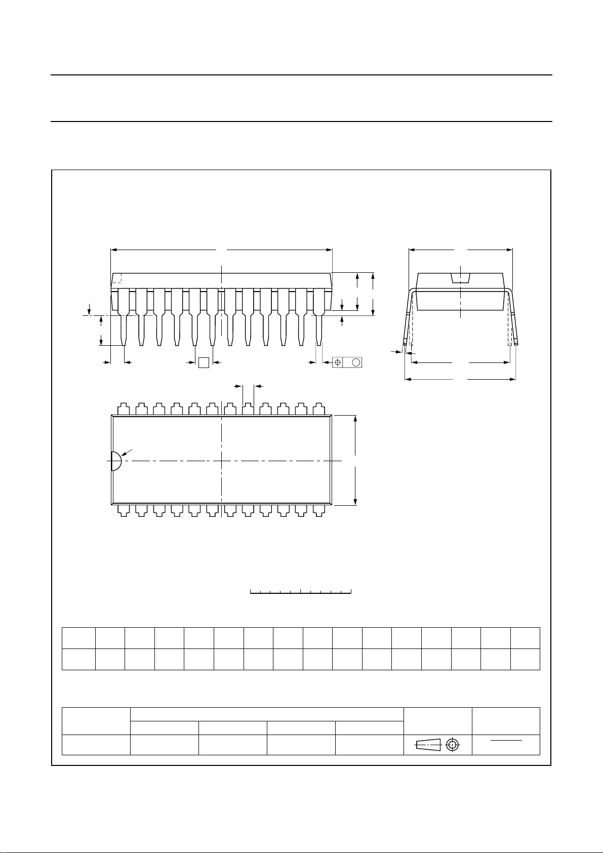
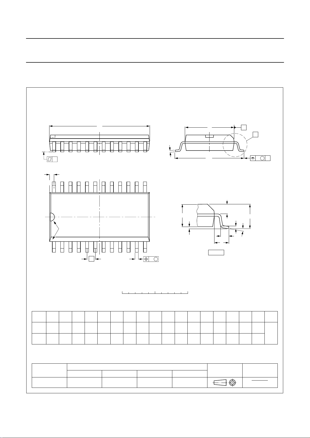
is 8 V. The device is mounted in a 24-lead SDIP package, or in a 24-lead SO package.
QUICK REFERENCE DATA
SYMBOL PARAMETER CONDITIONS MIN. TYP. MAX. UNIT
V
CC
V
i(Y)
V
i(UV)
V
FS(ADC)
ORDERING INFORMATION
TYPE
NUMBER
TDA9178 SDIP24 plastic shrink dual in-line package; 24 leads (400 mil) SOT234-1
TDA9178T SO24 plastic small outline package; 24 leads; body width 7.5 mm SOT137-1
supply voltage 7.2 8.0 8.8 V
luminance input voltage (excluding sync) AMS = 0 − 0.315 0.45 V
AMS = 1 − 1.0 1.41 V
UV input voltage −−1.9 V
full-scale ADC input voltage − 2.0 − V
PACKAGE
NAME DESCRIPTION VERSION
1999 Sep 24 3
Page 4
This text is here in white to force landscape pages to be rotated correctly when browsing through the pdf in the Acrobat reader.This text is here in
_white to force landscape pages to be rotated correctly when browsing through the pdf in the Acrobat reader.This text is here inThis text is here in
white to force landscape pages to be rotated correctly when browsing through the pdf in the Acrobat reader. white to force landscape pages to be ...
1999 Sep 24 4
n.c.12n.c.
handbook, full pagewidth
BLOCK DIAGRAM
Philips Semiconductors Preliminary specification
YUV one chip picture improvement based on luminance
vector-, colour vector- and spectral processor
DEC
YIN
UIN
VIN
DIG
V
CC
V
EE
SC
TP
ADR
SDA
SCL
6
8
9
15
20
18
1
10
7
14
11
13
INPUT
ST A GE
SUPPL Y
WINDOW
GENERA TION
CALIBRATE
Y
U, V
LUMINANCE
PROCESSING
black stretch
histogram processing
gamma control
colour vector
processing
SATURATION
CORRECTION
skin tone correction
green enhancement
blue stretch
NOISE
MEASURING
FEA TURE
MODE
DETECTION
CONTROL
PROCESSING
cue flash
I2C-BUS CONTROL
spectral processingluminance vector processing
SMART PEAKING
LUMINANCE TRANSIENT
IMPROVEMENT
VIDEO DEPENDENT
CORING
COLOUR DEPENDENT
SHARPNESS
DELA Y
COLOUR
COLOUR TRANSIENT
IMPROVEMENT
+
ANALOG
TO
DIGIT AL
CONVERTER
OUTPUT
STAGE
21
SOUT
19
YOUT
17
UOUT
16
VOUT
24
n.c.
23
n.c.
22
CF
2
n.c.
3
ADEXT1
4
ADEXT2
5
ADEXT3
TDA9178
Fig.1 Block diagram.
MGR897
Page 5
Philips Semiconductors Preliminary specification
YUV one chip picture improvement based on luminance
vector-, colour vector- and spectral processor
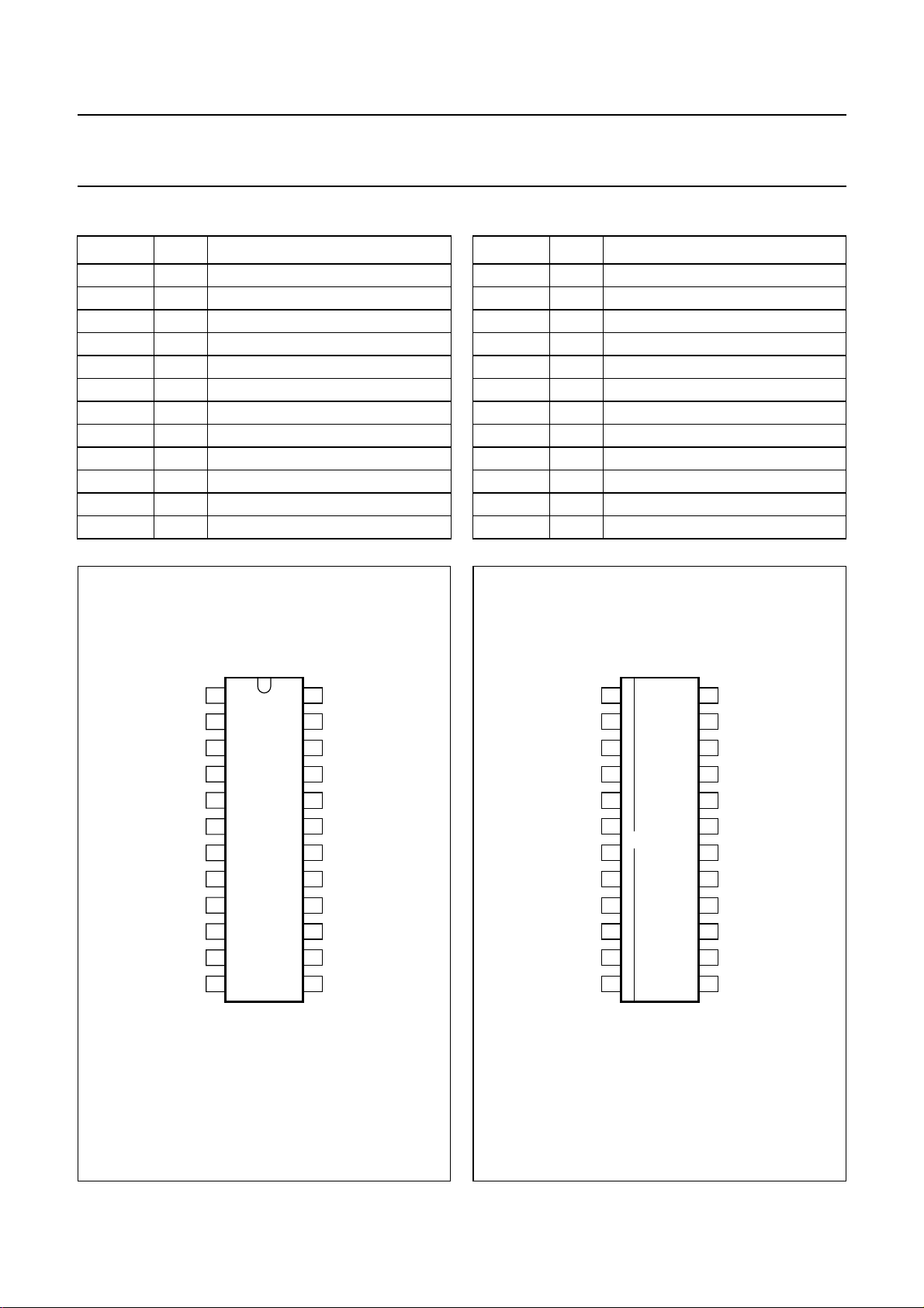
PINNING
SYMBOL PIN DESCRIPTION
SC 1 sandcastle input
n.c. 2 not connected
ADEXT1 3 ADC input 1
ADEXT2 4 ADC input 2
ADEXT3 5 ADC input 3
YIN 6 luminance input
ADR 7 address selection input
UIN 8 U signal input
VIN 9 V signal input
TP 10 test pin
SCL 11 serial clock input (I
2
C-bus)
n.c. 12 not connected
SYMBOL PIN DESCRIPTION
n.c. 13 not connected
SDA 14 serial data input/output (I
DEC
DIG
15 decoupling digital supply
VOUT 16 V signal output
UOUT 17 U signal output
V
EE
18 ground
YOUT 19 luminance output
V
CC
20 supply voltage
SOUT 21 SCAVEM output
CF 22 cue flash output
n.c. 23 not connected
n.c. 24 not connected
TDA9178
2
C-bus)
handbook, halfpage
SC
n.c.
ADEXT1
ADEXT2
ADEXT3
YIN
ADR
UIN
VIN
TP
SCL
n.c.
1
2
3
4
5
6
7
8
9
10
11
12
TDA9178
MGR898
n.c.
24
n.c.
23
CF
22
SOUT
21
V
20
CC
19
YOUT
V
18
EE
17
UOUT
VOUT
16
DEC
15
DIG
SDA
14
n.c.
13
handbook, halfpage
SC
n.c.
ADEXT1
ADEXT2
ADEXT3
YIN
ADR
UIN
VIN
TP
SCL
n.c.
1
2
3
4
5
6
TDA9178T
7
8
9
10
11
12
MGR899
n.c.
24
n.c.
23
CF
22
SOUT
21
V
20
CC
19
YOUT
V
18
EE
17
UOUT
VOUT
16
DEC
15
DIG
SDA
14
n.c.
13
Fig.2 Pin configuration (SOT234-1).
1999 Sep 24 5
Fig.3 Pin configuration (SOT137-1).
Page 6

Philips Semiconductors Preliminary specification
YUV one chip picture improvement based on luminance
vector-, colour vector- and spectral processor
FUNCTIONAL DESCRIPTION
Y input selection and amplification
The gain of the luminance input amplifier and output
amplifier can be adjusted to signal amplitudes of
0.315 and 1.0 V typically (excluding sync) by I2C-bus
bit AMS. The sync part is processed transparently to the
output, independently of the feature settings.
The Y, U and V input signals are clamped during the
burstkey period, defined by the sandcastle reference and
should be DC-coupled (the circuit uses internal clamp
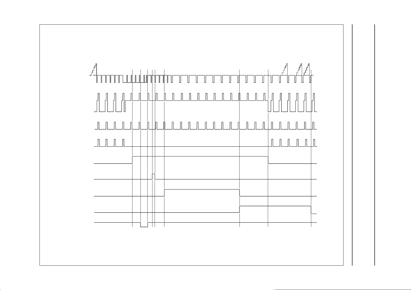
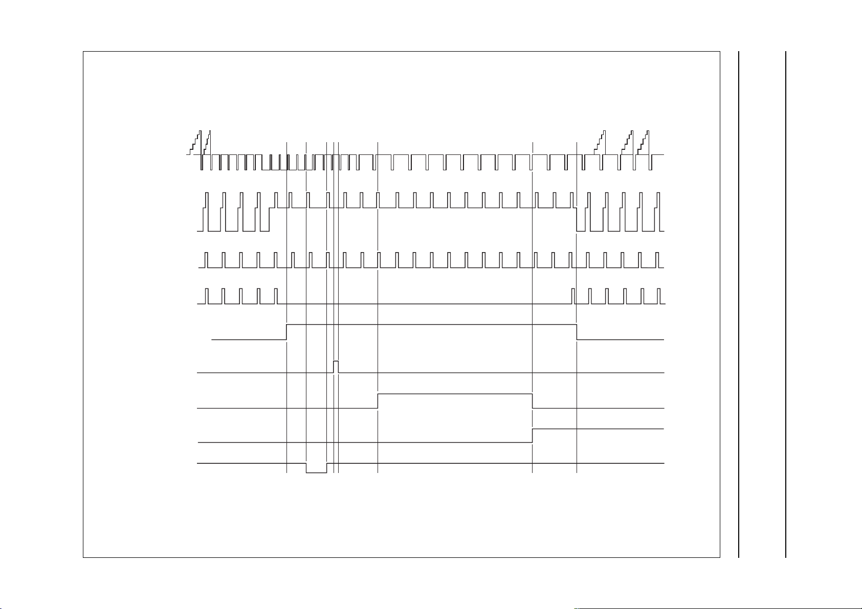
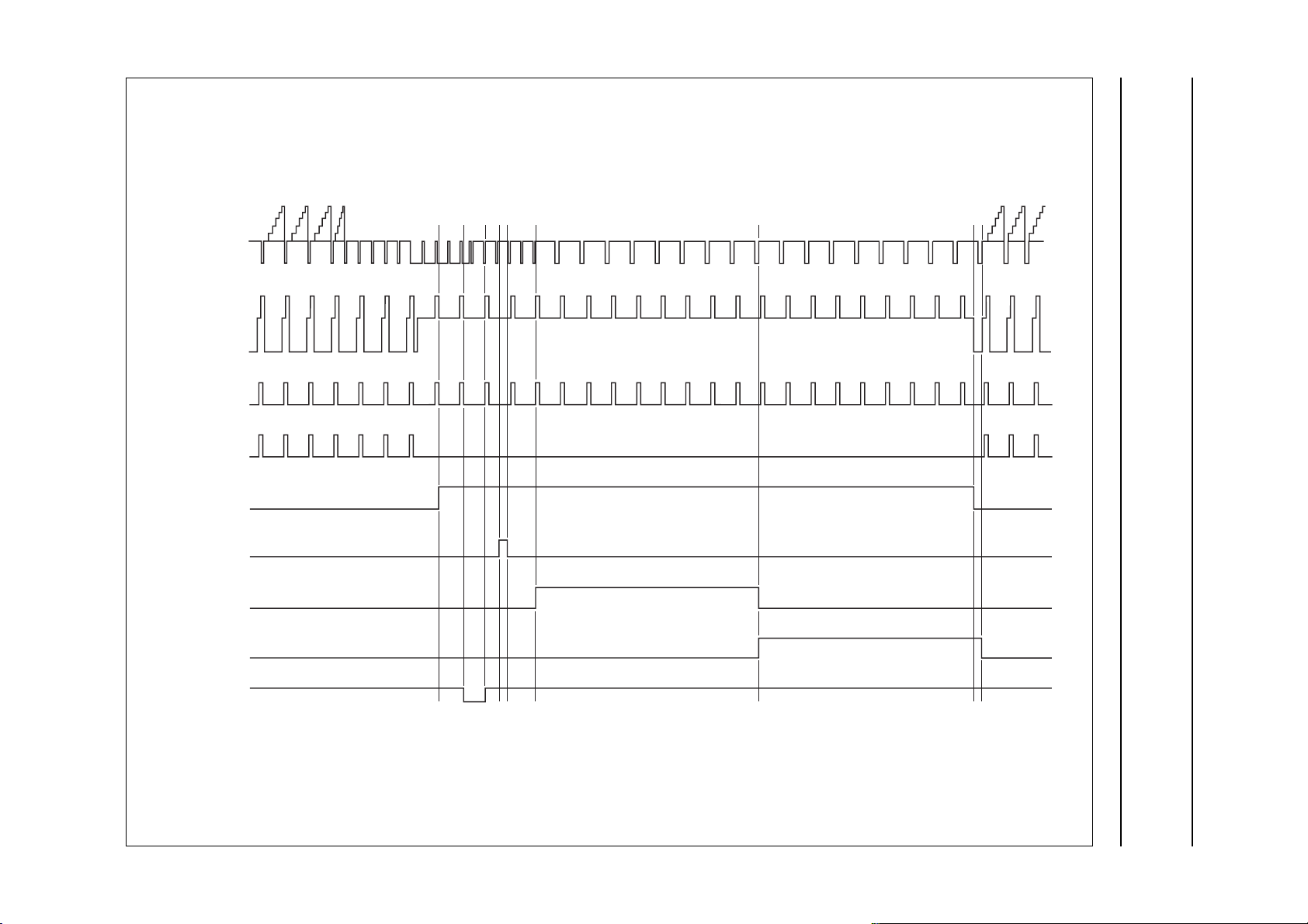
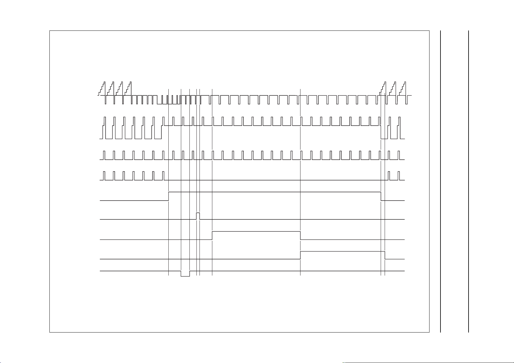
capacitors). During the clamp pulse (see Figs 7, 8, 9
and 10) an artificial black level is inserted in the Y input
signal to correctly preset the internal circuitry.
Luminance vector processor
Intheluminancevectorprocessorthetransfer is controlled
bya black stretch, the histogramprocessing and a gamma
control circuit. The luminance vector processor also
creates the cue flash signal.
BLACK STRETCH
Ablack detector measures and stores thelevelof the most
black part of the scene within an internal defined fixed
window in each field into a time constant. The time
constant and the response time of the loop are internally
fixed. Any difference between this value and the value
measured during the clamp is regarded as black offset.
In a closed loop offsets until a predefined value of the fullscale value are fed back to the input stage for
compensation.The loop gain is afunction of the histogram
and variable gamma settings. The black offset correction
can be switched on and off by the I2C-bus bit BON.
Related to the corrected black offset the nominal signal
amplitude is set again to 100% full scale through an
amplitude stretch function. Luminance values beyond full
scale are unaffected. Additionally, the measured black
offset is also used to set the adaptive black stretch gain
(see also Section “Adaptive black stretch”).
HISTOGRAM PROCESSING
For the luminance signal the histogram distribution is
measured in real-time over five segments within an
internally defined fixed window in each field. During the
period that the luminance is in one segment, a
corresponding internal capacitor is loaded by a current
source. At the end of the field five segment voltages are
stored into on-board memories. The voltages stored in the
memories determine the non-linear processing of the
luminance signal to achieve a picture with a maximum of
information (visible details).
Each field the capacitors are discharged and the
measurement starts all over again.
Parts in the scene that do not contribute to the information
inthatscene,likesub or side titles,should be omitted from
the histogram measurement. No measurements are
performed outside the internal fixed window period.
Very rapid picture changes, also related to the field
interlace,canresultinflickereffects.The histogram values
are averaged at the field rate thus cancelling the flicker
effects.
Adaptive black stretch
The so-called adaptive black stretch gain is one of the
factors that control the gamma of the picture. This gain is
controlled by the measured black offset value in the black
stretch circuit and theI2C-bus adaptive black stretchDAC:
bits BT5 to BT0. For pictures with no black offset the black
stretchgainequalsunitysothegammaisnotchanged and
the DAC setting has no influence. In case of a black offset,
the black stretch gain is increased so the gamma of the
pictureis reduced. This procedure results in amaximumof
visible details over the whole range of luminances.
However, depending on personal taste, sometimes higher
values of gamma are preferred. Therefore the amount of
gamma reduction can be adjusted by the DAC.
Adaptive white-point stretching
Forpictureswithmany details in white parts, the histogram
conversion procedure makes a transfer with large gain in
the white parts. The amount of light coming out of the
scene is reduced accordingly. The white stretcher
introduces additional overall gain for increased light
production, and so violating the principle of having a
full-scale reference. The white-point stretching can be
switched on or off by means of the I2C-bus bit WPO.
Standard deviation
Forscenesinwhichsegmentsofthehistogramdistribution
areverydominantwithrespecttotheothers,thenon-linear
amplification should be reduced in comparison to scenes
with a flat histogram distribution. The standard deviation
detectormeasuresthe spread of the histogram distribution
and modulates the user setting of the non-linear amplifier.
Non-linear amplifier
Thestoredsegmentvoltagesdeterminetheindividualgain
of each segment in such a way that continuity is granted
for the complete luminance range.
TDA9178
1999 Sep 24 6
Page 7

Philips Semiconductors Preliminary specification
YUV one chip picture improvement based on luminance
vector-, colour vector- and spectral processor
The maximum and minimum gain of each segment is
limited. Apart from the adaptive white-point stretching the
black and white references are not affected by the
non-linear processing. The amount of non-linearity can be
controlled by the I2C-bus non-linearity DAC:
bits NL5 to NL0.
VARIABLE GAMMA
On top of the histogram conversion a variable gamma
function is applied for an alternative brightness control, or
for factory adjustment. It is intended as an alternative for
the DC-offset of the classic brightness user control.
It maintains the black and white references. The gamma
ranges from 0.5 to 1.5. The gamma can be set by the
I2C-bus variable gamma DAC: bits VG5 to VG0.
CUE FLASH
In the present TV environment there is a lot of measured
information like ambient light and noise. This information
can be used to make an update of settings of the several
algorithms after a picture has changed. The cue flash
signal detects when a picture changes significantly. When
the picture content has changed, the I2C-bus bit CF is set
to logic 1 in the status register. After reading the status
register, bit CF is reset to logic 0. On the output pin CF the
cue flash information is present (active LOW) for only one
line in the vertical retrace part. This pin is configured as an
open drain output and therefore should be pulled up to the
5 V supply.
Spectral processor
In the spectral processor the luminance transfer is
controlled by smart peaking, colour dependent sharpness
and luminance transient improvement, defined by the
sharpness improvement processor. The colour transfer is
controlled by a colour transient improvement circuit; an
additional output is available to provide a SCAVEM circuit.
ADJUSTABLE CHROMINANCE DELAY
The colour vector processor drives a delay line for
correctingdelayerrors between the luminance input signal
and the chrominance input signals (U and V).
The chrominance delay can be adjusted in 6 steps of
12 ns (1fH) or 6 ns (2fH) by the I2C-bus bits CD2 to CD0.
It comprises three main processing units: the step
improvement processor, the contour processor and the
smart sharpness controller.
Transient improvement processor
The step improvement processor (see Fig.11) comprises
two main functions:
• MINMAX generator
• MINMAX fader.
The MINMAX generator utilizes all taps of an embedded
luminance delay line to calculate the minimum and
maximumenvelopeofallsignalsmomentarilystored in the
delay line. The MINMAX fader chooses between the
minimum and maximum envelopes, depending on the
polarity of a decision signal derived from the contour
processor. Figures 12, 13 and 14 show some waveforms
of the step improvement processor and illustrate that fast
transients result with this algorithm. The MINMAX
generator also outputs a signal that represents the
momentary envelope of the luminance input signal.
This envelope information is used by the smart sharpness
controller.
Line width control (also called aperture control) can be
performed by I2C-bus line width DAC: bits LW5 to LW0.
This control can be used to compensate for horizontal
geometryerrorscausedby the gamma, for blooming of the
spot of the CRT, or for compensating SCAVEM.
Contour processor
The contour processor comprises two contour generators
with different frequency characteristics. The contour
generator generates a second-order derivative of the
incoming luminance signal which is supplied to the smart
sharpness controller. In the smart sharpness controller,
this signal is added to the properly delayed original
luminance input signal, making up the peaking signal for
detail enhancement. The peaking path features a low
peaking frequency of 2 MHz (at 1fH), or a high peaking
frequency of 3 MHz (at 1fH), selectable by I2C-bus
bit CFS.
The contour generators utilize three taps of the embedded
luminance delay line. Figure 15 illustrates the normalized
frequency transfer of the filter.
TDA9178
SHARPNESS IMPROVEMENT PROCESSOR
The sharpness improvement processor increases the
slope of large luminance transients of vertical objects and
enhancestransientsofdetailsinnaturalscenesbycontour
correction.
1999 Sep 24 7
Page 8

Philips Semiconductors Preliminary specification
YUV one chip picture improvement based on luminance
vector-, colour vector- and spectral processor
Smart sharpness controller
The smart sharpness controller (see Fig.16) is a fader
circuit that fades between peaked luminance and
step-improved luminance, controlled by the output of a
step discriminating device known as the step detector.
It also contains a variable coring level stage.
The step detector is basically a differentiator, so both
amplitude of the step and its slope add to the detection
criterion. The smart sharpness controller has four user
controls:
• Steepness control, performed by the I2C-bus DAC:
bits SP5 to SP0
• Peaking control, performed by the I2C-bus DAC:
bits PK5 to PK0
• Video dependent coring, switched on or switched off by
the I2C-bus bit VDC
• Coring level control, performed by the I2C-bus DAC:
bits CR5 to CR0.
Thesteepness setting controls the amountof steepness in
the edge-correction processing path.
The peaking setting controls the amount of contour
correction for proper detail enhancement. The envelope
signal generated by the step improvement processor
modulates the peaking setting in order to reduce the
amount of peaking for large sine wave excursions.
With video dependent coring, it is possible to have more
reduction of the peaking in the black parts of a scene than
inthewhiteparts,andthereforeautomaticallyreducing the
visibility of the background noise.
The coring setting controls the coring level in the peaking
path for rejection of high-frequency noise.
All four settings facilitate reduction of the impact of the
sharpness features, e.g. for noisy luminance signals.
COLOUR DEPENDENT SHARPNESS
The colour dependent sharpness circuit increases the
luminance sharpness in saturated red and magenta parts
of the screen. Because of the limited bandwidth of the
colour signals, there is no need to increase the high
frequenciesofthecolour signals. Instead, the details in the
luminance signal will be enhanced. In this circuit a limited
number of colours are enhanced (red and magenta).
Contrarytonormal peaking algorithm, extra gain is applied
for low frequencies (2 MHz at 1fH). This is needed,
because the information that is lacking below 2 MHz (at
1fH) is most important. In large coloured parts the normal
peaking is still active to enhance the fine details.
The smart peaking algorithm has been designed such that
the luminance output amplitude will never exceed 110% of
the luminance input signal amplitude. Therefore the
normal peaking range (12 dB) will be reduced at large
transients, and in case of colour dependent sharpness
there is even more reduction.
However, by setting bit OSP (Overrule Smart Peaking)
onecan undo the extra peaking reduction in case ofcolour
dependant sharpness. It must be emphasized that setting
OSP may lead to unwanted large luminance output
signals, for instance in details in red coloured objects.
COLOUR TRANSIENT IMPROVEMENT
The colour transient improvement circuit (see Fig.17)
increases the slope of the colour transients of vertical
objects. Each channel of the CTI circuit basically consists
oftwodelaycells:anelectronicpotentiometerandanedge
detector circuit that controls the wiper position of the
potentiometer.Normally the wiper of the potentiometerwill
be in position B (mid position), so passing the input
signal B to the output with a single delay. The control
signal is obtained by the signals A and C.
When an edge occurs the value of the control signal will
fade between +1 and −1 and finally will become zero
again. A control signal value of +1 fades the wiper in
position C, passing the two times delayed input signal to
the output. A control signal of −1 fades the wiper in
position A, so an undelayed input signal is passed to the
output. The result is an output signal which has steeper
edges than the input signal. Contrary to other existing
CTI algorithms, the transients remain time correct with
respect to the luminance signal, as the algorithm steepens
edges proportionally, without discontinuity.
SCAVEM
A luminance output is available for SCAVEM processing.
This luminance signal is not affected by the spectral
processing functions.
Colour vector processor
The colour processing part contains skin tone correction,
green enhancement and blue stretch. The colour vector
processing is dependent on the amplitude and sign of the
colour difference signals. Therefore, both the polarity and
the nominal amplitude of the colour difference signals are
relevant when using the colour vector processor facility.
TDA9178
1999 Sep 24 8
Page 9

Philips Semiconductors Preliminary specification
YUV one chip picture improvement based on luminance
vector-, colour vector- and spectral processor
SKIN TONE CORRECTION
Skintones are very sensitive fortransmission (hue) errors,
because we have an absolute feeling for skin tones.
To make a picture look free of hue error, the goal is to
make sure that skin tones are put at a correct colour.
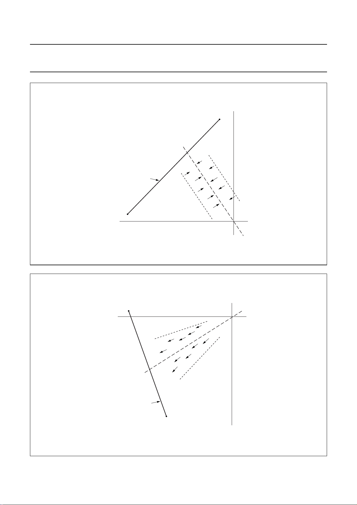
The dynamic skin tone correction circuit achieves this goal
by instantaneously and locally changing the hue of those
colours which are located in the area in the UV plane that
matches skin tones (see Fig.4).
The correction is dependent on luminance, saturation and
distance to the preferred axis and can be done towards
twodifferentangles.Thepreferredanglecanbechosenby
bit ASK in the I2C-bus settings. The settings are
123° (ASK = 0) and 117° (ASK = 1). The enclosed
correction area can be increasedto 140% with the I2C-bus
bit SSK(so-called:Size).Theencloseddetection‘angle’of
the correcting area can be increased to 160% with the
I2C-bus bit WSK (so-called: Width). The skin tone
correction can be switched on or off with the I2C-bus
bit DSK.
GREEN ENHANCEMENT
The green enhancement circuit (see Fig.5) is intended to
shift low saturated green colours towards more saturated
green colours. This shift is achieved by instantaneously
andlocallychangingthosecolourswhicharelocatedinthe
area in the UV plane that matches low saturated green.
The saturation shift is dependent on the luminance,
saturation and distance to the detection axis of 208°.
The direction of shift in the colour is fixed by hardware.
The amount of green enhancement can be increased to
160% by the I2C-bus bit GGR. The enclosed detection
‘angle’ of the correcting area can be increased to 160%
withthe I2C-busbit WGR (so-called: Width). The enclosed
correction area can be increasedto 140% with the I2C-bus
bit SGR (so-called: Size). The green enhancement can be
switched on or switched off with the I2C-bus bit DGR.
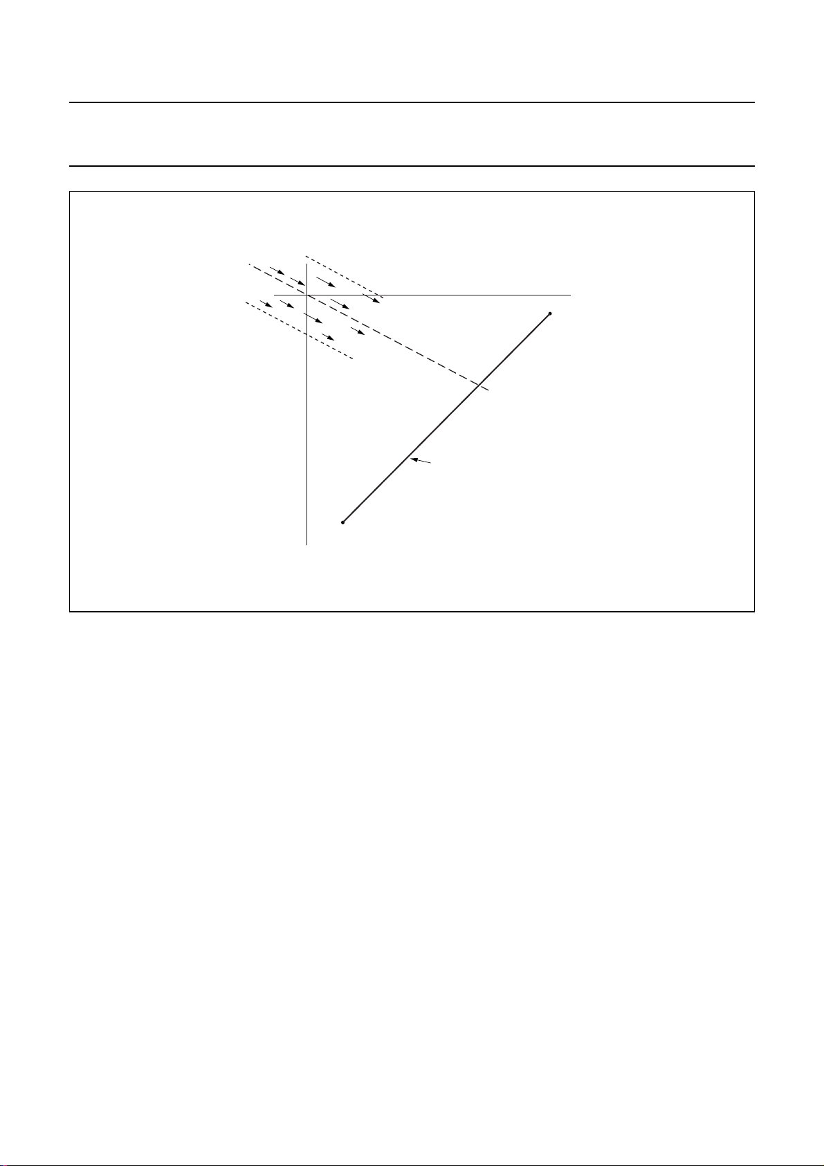
BLUE STRETCH
The blue stretch circuit (see Fig.6) is intended to shift
colours near white towards more blueish coloured white to
give a brighter impression. This shift is achieved by
instantaneously and locally changing those colours which
are located in the area in the UV plane that matches
colours near white. The shift is dependent on the
luminance and saturation. The direction of shift (towards
an angle of 330°) in the colour is fixed by hardware.
The amount of blue stretch can be increased to 160% by
the I2C-bus bit GBL.
Theenclosedcorrectionareacanbeincreasedto140%by
the I2C-bus bit SBL (so-called: Size). The blue stretch can
be switched on or off by the I2C-bus bit DBL.
SATURATION CORRECTION
The non-linear luminance processing done by the
histogram modification and variable gamma, influences
the colour reproduction; mainly the colour saturation.
Therefore, the U and V signals are linear processed for
saturation compensation.
Noise measuring
A video line which is supposed to be free from video
information(‘emptyline’)is used to measure the amount of
noise. The measured RMS value of the noise can be used
for reducing several features, by the I
such as luminance vector processing and spectral
processing. For the TDA9178 the empty line is chosen
three lines after recognition of the vertical blanking from
the sandcastle pulse input. Figures 7, 8, 9 and 10 show
the measurement locations for different broadcast norms.
The noise detector is capable of measuring the
signal-to-noise ratio between −45 and −20 dB. The output
scale runs linearly with dB. The noise samples are
averagedforover20 fields to reduce the fluctuations in the
measurement process. It is obvious, that for signal
sources (like VCR in still picture mode) that re-insert the
levels of the retrace part, the measurement is not reliable
(see Section “Feature mode detector”). The result of the
averaging process will update the contents of the I
register: bits ND5 to ND0 at a rate of
frequency. If a register access conflict occurs, the data of
the noise register is made invalid by setting the flag bit DV
(Data Valid) to zero.
Feature mode detector
A detector is available for detecting signal sources (like
VCR in still picture mode) that re-inserted the levels of the
retrace part. For this kind of signals the noise
measurement of the TDA9178 is not reliable, but this
detector sets bit FM in the ND-register to logic 1.
For normal video signals bit FM is set to logic 0.
This circuit measures transients (like synchronization
pulses) on the luminance input during the internal V-pulse.
Thefeaturemodedetector is setting bit FM to logic 1 when
no transients are present during 2 lines in the vertical
retrace part over 3 fields (like the synchronization pulses).
TDA9178
2
C-bus interface,
2
1
⁄32 of the field
C-bus
1999 Sep 24 9
Page 10

Philips Semiconductors Preliminary specification
YUV one chip picture improvement based on luminance
vector-, colour vector- and spectral processor
Successive approximation ADC
Pins ADEXT1, ADEXT2 and ADEXT3 are connected to a
6-bit successive approximation ADC via a multiplexer.
The multiplexertogglesbetweentheinputswitheachfield.
At each field flyback, a conversion is started for two of the
three inputs and the result is stored in the corresponding
bus register ADEXT1, ADEXT2 or ADEXT3. The input pin
ADEXT1 is updated every field, while input fields
ADEXT2 and ADEXT3 are updated once in two
consecutive fields (see Figs 7, 8, 9 and 10). Once in
32 fields the ADEXT2 input is not updated, because then
the noise measurement is updated.
In this way, any slow varying analog signal can be given
access to the I2C-bus. If a register access conflict occurs,
the data of that register is made invalid by setting the flag
bit DV (Data Valid) to zero.
Smart noise control
With the help of the internal noise detector and a
user-preferred noise algorithm, the user can make a fully
automatic I2C-bus feature reduction, briefly called ‘Smart
Noise Control’.
I2C-bus
The I2C-bus is always instandby mode and responds on a
properly addressed command. Bit PDD (Power-Down
Detected) in the status register is set each time an
interruptionofthe power supply occurs and is reset only by
reading the status register. A 3-bit identification code can
also be read from the status register, which code can be
used to automatically configure the application by
software.
The input control registers can be written sequentially by
the I2C-bus by the embedded automatic subaddress
increment feature or by addressing them directly.
The output control functions cannot be addressed
separately. Reading out the output control functions
always starts at subaddress 00H and all subsequent
words are read out by the automatic subaddress
increment procedure.
The bits in the I2C-bus are preset to logic 0 at power-on
except for bits AMS and VG5: therefore the TDA9178 is in
1.0 V luminance signal range and the variable gamma is
set to 20H (gamma correction 0%).
TDA9178
Demonstration mode
By the I2C-bus bit DEM all the picture improvement
features can be demonstrated in one picture. By setting
bit DEM to logic 1, all the features selected bythe user are
active for 5 s in 1fH mode (in 2fH mode: 2.5 s), and for
another 5 s in 1fH mode (in 2fH mode: 2.5 s) all features
selected are turned off (then the TDA9178 is ‘transparent’
to the incoming signal).
Internal window
To determine the histogram levels and the black offset the
TDA9178 performs several measurements. An internally
defined window serves to exclude parts in the scene like
‘subtitling’ or ‘logos’. The internal window can be regarded
as a weighting function which has a value of one within a
square near the centre of the screen and which gradually
decreases to zero towards the edges.
When bit WLB (Window Letter Box) is made logic 1, the
2
height of the window is reduced by a factor of
This prevents the contribution of the black bars above and
below a 16 : 9 scene to the measurements.
⁄3.
2
I
C-BUS SPECIFICATION
The slave address of the IC is given in Table “Slave
address”. If pin ADR of the TDA9178 is connected to
ground, the I2C-bus address is 40H; if pin ADR is
connected to pin DEC
The circuit operates on clock frequencies up to 400 kHz.
Slave address
A6 A5 A4 A3 A2 A1 A0 R/W
ADR 1 ADR 0 0 0 0 X
Auto-increment mode is available for subaddresses.
, the I2C-bus address is E0H.
DIG
1999 Sep 24 10
Page 11

Philips Semiconductors Preliminary specification
YUV one chip picture improvement based on luminance
TDA9178
vector-, colour vector- and spectral processor
Control functions
FUNCTIONS TYPE SUBADDRESS
D7 D6 D5 D4 D3 D2 D1 D0
Inputs
Control 1 REG 00 DEM VDC WLB FHS CFS LDH 0 AMS
Control 2 01 0 0 OSP WPO 0 CD2 CD1 CD0
Control 3 02 SGR WGR GGR DGR SSK WSK ASK DSK
Control 4 03 0 0 BON CTI CDS SBL GBL DBL
Adaptive black stretch DAC 04 0 0 BT5 BT4 BT3 BT2 BT1 BT0
Non-linearity amplifier 05 0 0 NL5 NL4 NL3 NL2 NL1 NL0
Variable gamma 06 0 0 VG5 VG4 VG3 VG2 VG1 VG0
Peaking 07 0 0 PK5 PK4 PK3 PK2 PK1 PK0
Steepness 08 0 0 SP5 SP4 SP3 SP2 SP1 SP0
Coring 09 0 0 CR5 CR4 CR3 CR2 CR1 CR0
Line width 0A 0 0 LW5 LW4 LW3 LW2 LW1 LW0
Outputs
Status REG 00 X X X CF ID2 ID1 ID0 PDD
Noise detection 01 FM DV ND5 ND4 ND3 ND2 ND1 ND0
ADEXT1 (output) 02 X DV AD5 AD4 AD3 AD2 AD1 AD0
ADEXT2 (output) 03 X DV AD5 AD4 AD3 AD2 AD1 AD0
ADEXT3 (output) 04 X DV AD5 AD4 AD3 AD2 AD1 AD0
DATA BYTE
1999 Sep 24 11
Page 12

Philips Semiconductors Preliminary specification
YUV one chip picture improvement based on luminance
vector-, colour vector- and spectral processor
Input signals
Table 1 Amplitude mode selection
AMS FUNCTION
0 0.315 V luminance (black to white) at
YIN
1 1.0 V luminance (black to white) at YIN
Table 2 Luminance determined histogram
LDH FUNCTION
0 histogram segments fixed
1 histogram segments determined by peak
white
Table 3 Contour filter selection
CFS FUNCTION
0 peaking frequency is 2 MHz at 1f
4 MHz at 2f
H
1 peaking frequency is 3 MHz at 1fHor
6 MHz at 2f
H
Table 4 Line frequency selection
or
H
Table 8 Chrominance delay
CD2 CD1 CD0 FUNCTION
0 0 0 40 ns at 1f
111−32 ns at 1fHor +16 ns at 2f
Table 9 Overrule smart peaking
OSP FUNCTION
0 smart peaking (maximum peaking
reduced if Coxing)
1 overrule smart peaking
Table 10 White-point stretch on/off
WPO FUNCTION
0 white-point stretch on
1 white-point stretch off
Table 11 Dynamic skin tone on/off
DSK FUNCTION
0 skin tone off
1 skin tone on
TDA9178
or 20 ns at 2f
H
H
H
FHS FUNCTION
01f
12f
H
H
Table 5 Window letterbox format
WLB FUNCTION
0 normal internal window format
1 ‘Letterbox’ internal window format
Table 6 Video dependent coring on/off
VDC FUNCTION
0 video dependent coring off
1 video dependent coring on
Table 7 Demonstration mode on/off
DEM FUNCTION
0 DEMO off
1 DEMO on: auto-toggle selected features
on/off (cycle is 10 s at 1fHor 5 s at 2fH)
Table 12 Dynamic skin tone angle
ASK FUNCTION
0 angle correction 123°
1 angle correction 117°
Table 13 Dynamic skin tone width
WSK FUNCTION
0 default detection angle
1 60% increased detection angle
Table 14 Dynamic skin tone size
SSK FUNCTION
0 default area
1 40% increased area
Table 15 Green enhancement on/off
DGR FUNCTION
0 green enhancement off
1 green enhancement on
1999 Sep 24 12
Page 13

Philips Semiconductors Preliminary specification
YUV one chip picture improvement based on luminance
vector-, colour vector- and spectral processor
Table 16 Green enhancement gain
GGR FUNCTION
0 default enhancement
1 60% increased gain
Table 17 Green enhancement width
WGR FUNCTION
0 default detection angle
1 60% increased detection angle
Table 18 Green enhancement size
SGR FUNCTION
0 default area
1 40% increased area
Table 19 Blue stretch on/off
Table 24 Black offset compensation on/off
BON FUNCTION
0 black offset compensation off
1 black offset compensation on
Table 25 Adaptive black stretch
BT5 BT4 BT3 BT2 BT1 BT0 FUNCTION
0000000%
111111100%
Table 26 Non-linearity amplifier
NL5 NL4 NL3 NL2 NL1 NL0 FUNCTION
0000000%
111111100%
Table 27 Variable gamma
TDA9178
DBL FUNCTION
0 blue stretch off
1 blue stretch on
Table 20 Blue stretch gain
GBL FUNCTION
0 default gain
1 60% increased gain
Table 21 Blue stretch size
SBL FUNCTION
0 default area
1 40% increased area
Table 22 Colour dependent sharpness on/off
CDS FUNCTION
0 colour dependent sharpness off
1 colour dependent sharpness on
Table 23 Colour transient improvement on/off
VG5 VG4 VG3 VG2 VG1 VG0 FUNCTION
000000−100%
111111100%
Table 28 Peaking amplitude
PK5 PK4 PK3 PK2 PK1 PK0 FUNCTION
0000000%
111111100%
Table 29 Steepness correction
SP5 SP4 SP3 SP2 SP1 SP0 FUNCTION
0000000%
111111100%
Table 30 Coring level
CR5 CR4 CR3 CR2 CR1 CR0 FUNCTION
0000000%
11111130%
CTI FUNCTION
0 colour transient improvement off
1 colour transient improvement on
1999 Sep 24 13
Page 14

Philips Semiconductors Preliminary specification
YUV one chip picture improvement based on luminance
vector-, colour vector- and spectral processor
Table 31 Line width correction
LW5 LW4 LW3 LW2 LW1 LW0 FUNCTION
00000033% duty
factorat2 MHz
sine wave/1f
11111167% duty
factorat2 MHz
sine wave/1f
Output signals
Table 32 Power-down detection
PDD FUNCTION
0 no power-down detected since last read
1 power-down detected
Table 33 Identification code
ID2 ID1 ID0 FUNCTION
0 1 0 TDA9178/N1
H
H
Table 35 Noise detector
ND5 ND4 ND3 ND2 ND1 ND0 FUNCTION
000000−45 dB
111111−20 dB
Table 36 ADEXT1, ADEXT2 and ADEXT3
AD5 AD4 AD3 AD2 AD1 AD0 FUNCTION
000000external
111111external
Table 37 Data valid bit of
noise detector/ADEXT1, 2 and 3 registers
DV FUNCTION
0 data not valid because of possible register
access collision
1 data is valid
TDA9178
voltage = 0 V
voltage = 2 V
Table 34 Cue flash
CF FUNCTION
0 no cue flash since last read
1 cue flash detected
Table 38 Feature mode detector
FM FUNCTION
0 normal video signal detected
1 feature mode detected (noise detector is
not reliable)
LIMITING VALUES
In accordance with the Absolute Maximum Rating System (IEC 134); all voltages referenced to ground.
SYMBOL PARAMETER MIN. MAX. UNIT
V
CC
V
n
T
stg
T
amb
T
j
supply voltage −0.5 +8.8 V
voltage on any pin −0.5 VCC+ 0.5 V
storage temperature −55 +150 °C
operating ambient temperature −10 +70 °C
operating junction temperature − 150 °C
HANDLING
All pins are protected against ESD by means of internal clamping diodes. The protection circuit meets the following
specification:
Human body model: C = 100 pF; R = 1.5 kΩ; all pins >3000 V
Machine model: C = 200 pF; R = 0 Ω; all pins >200 V.
At an ambient temperature of 90 °C, all pins meet the following specification:
I
> 100 mA or V
trigger
I
< −100 mA or V
trigger
pin
pin
> 1.5V
< −0.5V
CC(max)
CC(max)
1999 Sep 24 14
Page 15

Philips Semiconductors Preliminary specification
YUV one chip picture improvement based on luminance
TDA9178
vector-, colour vector- and spectral processor
THERMAL CHARACTERISTICS
SYMBOL PARAMETER CONDITIONS VALUE UNIT
R
th(j-a)
QUALITY SPECIFICATION
In accordance with
CHARACTERISTICS
VCC=8V; T
SYMBOL PARAMETER CONDITIONS MIN. TYP. MAX. UNIT
Supply
S
UPPLY VOLTAGE (PIN V
V
CC
I
CC
DIGITAL SUPPLY DECOUPLING (PIN DEC
V
DECDIG
I
DECDIG
Input and output selection
thermal resistance from junction to ambient in free air
TDA9178 (SDIP24) 56 K/W
TDA9178T (SO24) 65 K/W
“SNW-FQ-611 part E”
=25°C; unless otherwise specified.
amb
)
CC
.
supply voltage 7.2 8.0 8.8 V
supply current 1fH mode − 100 − mA
2f
mode − 105 − mA
H
)
DIG
decoupling voltage − 5 − V
decoupling load current −−1mA
LUMINANCE INPUT (PIN YIN)
V
i(Y)
I
i(bias)(Y)
input voltage (excluding sync) AMS = 0 − 0.315 0.45 V
input bias current no clamp −−0.1 µA
LUMINANCE OUTPUT (PIN YOUT)
V
o(cl)
output voltage level during
clamping
G
Y(i-o)
luminance gain input to output transparent
S/N(Y) signal-to-noise ratio of luminance
output
B
Y
E
bl
luminance bandwidth 1fH mode (−1 dB);
black level error transparent −1.0 0 +1.0 %
AMS = 1 − 1.0 1.41 V
AMS = 1 − 2.7 − V
AMS = 0 − 0.8 − V
0.93 1.04 1.15
at AMS = 1;
at 1 V (p-p)
transparent
0.96 1.07 1.18
at AMS = 0;
at 0.3 V (p-p)
transparent 52 −−dB
5 −−MHz
transparent
2f
mode (−1 dB);
H
6 −−MHz
transparent
1999 Sep 24 15
Page 16

Philips Semiconductors Preliminary specification
YUV one chip picture improvement based on luminance
TDA9178
vector-, colour vector- and spectral processor
SYMBOL PARAMETER CONDITIONS MIN. TYP. MAX. UNIT
R
o
I
o(bias)
C
L
COLOUR DIFFERENCE INPUTS U AND V(PINS UIN AND VIN)
V
i(U)(p-p)
V
i(V)(p-p)
I
i(bias)
COLOUR DIFFERENCE OUTPUTS U AND V(PINS UOUT AND VOUT)
V
o(cl)
G
UV(i-o)
E
offset
∆G
track
B
UV
R
o
I
o(bias)
C
L
Luminance vector processing
output resistance −−150 Ω
output bias current 1.3 −−mA
load capacitance −−15 pF
input voltage U
− 1.33 1.9 V
(peak-to-peak value)
input voltage V
− 1.05 1.9 V
(peak-to-peak value)
input bias current no clamp −−0.1 µA
output voltage level during
− 2.7 − V
clamping
gain inputs to output transparent 0.90 1.00 1.10
offset error transparent −1 0 +1 %
UV gain tracking error transparent −−5%
bandwidth 1fH mode;
2.5 −−MHz
transparent (−3 dB)
2f
mode;
H
5 −−MHz
transparent (−3 dB)
output resistance −−150 Ω
output bias current 1.3 −−mA
load capacitance −−15 pF
BLACK STRETCH
BLOS
cor(i)
input black offset correction 8 10 12 %
HISTOGRAM
White-point stretch
G
WP(max)
maximum luminance gain for white
stretch
maximum non-linearity
setting gain
Non-linear amplifier
G
nla(min)
minimum segment gain maximum non-linearity
setting gain
G
nla(max)
maximum segment gain maximum non-linearity
setting gain
G
nla
non-linear control curve 63 steps − 0 to 100 − %
VARIABLE GAMMA
G
g(var)(min)L
G
g(var)(max)
G
nla
minimum variable gamma setting − 0.5 −
maximum variable gamma setting − 1.5 −
non-linear control curve 63 steps − 0 to 100 − %
1999 Sep 24 16
− 1.1 −
− 0.4 −
− 2.0 −
Page 17

Philips Semiconductors Preliminary specification
YUV one chip picture improvement based on luminance
TDA9178
vector-, colour vector- and spectral processor
SYMBOL PARAMETER CONDITIONS MIN. TYP. MAX. UNIT
Colour vector processing
SKIN TONE; note 1 and Fig.4
ϕ
cor
ϕ
ap
GREEN ENHANCEMENT; note 1 and Fig.5
ϕ
cor
ϕ
ap
BLUE STRETCH; note 2 and Fig.6
ϕ
(str)
Spectral processing
GENERAL
Q
max
Contour filter low frequency peaking
f
pc(l)
Contour filter high frequency peaking
f
pc(h)
Step detector
f
dc
PEAKING
G
PK
CORING
G
CR
LUMINANCE TRANSIENT IMPROVEMENT
t
r(min)
G
SP
Line width control
t
sd(max)
G
LW
correction angle ASK = 0; DSK = 1 − 123 − deg
ASK = 1; DSK = 1 − 117 − deg
correction range (or aperture angle) DSK = 1; SSK = 1;
− 45 − deg
WSK = 0
correction angle DGR = 1 − 208 − deg
correction range (or aperture angle) DGR = 1; SGR = 0;
− 45 − deg
WGR = 0
stretch angle DBL = 1 − 330 − deg
maximum contour amplitude at
note 3 − 12 − dB
centre frequency
peaking centre frequency 1fH mode; CFS = 0 − 2.0 − MHz
2f
mode; CFS = 0 − 4.0 − MHz
H
peaking centre frequency 1fH mode; CFS = 1 − 3.0 − MHz
2f
mode; CFS = 1 − 6.0 − MHz
H
detection centre frequency 1fH mode − 1.18 − MHz
2f
mode − 2.36 − MHz
H
peaking control curve 63 steps − 0 to 100 − %
coring control curve 63 steps − 0to45 − %
minimum rise time 10% to 90% note 4 − 30 − ns
steepness control curve 63 steps − 0 to 100 − %
maximum step displacement 1fH mode − 140 − ns
2f
mode − 70 − ns
H
line width control curve (duty factor) 63 steps at 1 MHz
sine wave at 1f
H
− 33 to 67 − %
1999 Sep 24 17
Page 18

Philips Semiconductors Preliminary specification
YUV one chip picture improvement based on luminance
TDA9178
vector-, colour vector- and spectral processor
SYMBOL PARAMETER CONDITIONS MIN. TYP. MAX. UNIT
COLOUR TRANSIENT IMPROVEMENT
t
r(min)
COLOUR DEPENDENT SHARPNESS
f
pc
Q
max
SCAVEM
SCAVEM OUTPUT (PIN SOUT)
V
o(cl)
G
Y
B
Y
R
o
I
o(bias)
C
L
t
d(SOUT-YOUT)
Successive approximation ADC
minimum rise time 10% to 90% note 5 − 50 − ns
peaking centre frequency 1fH mode − 2.0 − MHz
2f
mode − 4.0 − MHz
H
maximum contour amplitude at
note 3 − 6 − dB
centre frequency
output voltage level during
− 2.2 − V
clamping
gain luminance input to SCAVEM
0.93 1.04 1.15
output
bandwidth 1fH mode (−1 dB) 5 −−MHz
2f
mode (−1 dB) 6.0 −−MHz
H
output resistance −−150 Ω
output bias current 0.8 −−mA
load capacitance −−15 pF
delay w.r.t. YOUT −−20 − ns
ADC INPUTS (PINS ADEXT1, ADEXT2 AND ADEXT3)
V
FS
I
i(bias)
full-scale input voltage range with respect to ground − 2.0 − V
input bias current −−0.1 µA
RES data path resolution − 6 − bit
DLE differential linearity error −−1 LSB
ILE integral linearity error −−1 LSB
f
Q
con
adt
conversion frequency ADEXT1 − 1f
ADEXT2; ADEXT3 − 0.5f
V
V
− Hz
− Hz
conversion time (video lines) each channel − 8 − lines
Timing
SANDCASTLE INPUT (PIN SC)
I
i(bias)
V
sc(bn)
V
sc(bc)
t
W(bk)
t
V
V
bk(var)(p-p)
input bias current −−1µA
detection level for blank no clamping 0.9 1.15 1.40 V
detection level for clamp − 0.9V
top
− V
burst key pulse width 1fH mode 1.8 −−µs
mode 0.9 −−µs
2f
H
vertical retrace time 6 −−lines
ripple on sandcastle burst key level
−−0.04V
top
V
(peak-to-peak value)
1999 Sep 24 18
Page 19

Philips Semiconductors Preliminary specification
YUV one chip picture improvement based on luminance
TDA9178
vector-, colour vector- and spectral processor
SYMBOL PARAMETER CONDITIONS MIN. TYP. MAX. UNIT
Overall output group delay performance
t
d(YUV)
t
dm(UV-Y)
Noise measurement
R
noise
t
con
Cue flash
CUE FLASH OUTPUT (PIN CF); OPEN COLLECTOR
V
o(max)
I
sink(max)
Notes
1. The amount of correction depends on the parameters of the incoming YUVsignals; therefore it is not possible to give
exact figures for the correction angle. The aperture angle of the correction range of 45° (±22.5°) is just given as an
indication and is valid for an input signal with a luminance signal amplitude of 75% and a colour saturation of 50%.
2. The amount of correction depends on the parameters of the incoming YUVsignals; therefore it is not possible to give
exact figures for the correction angle.
3. The contour signal cannot be measured separately from the luminance input signal. The contour signal is also
processed by the smart noise controller. The frequency transfer in the peaking mode of the luminance signal can be
derived from the frequency transfer of the selected contour signal, taking into account the summation of the contour
signal and the luminance input signal. The frequency transfer is most easily measured by sine excitation with a
relatively small signal amplitude of 10% of the selected dynamic range of the luminance input, to avoid interaction
with the step detector.
4. Peaking set to minimum. Input signal is a sine wave with the nominal peak-to-peak amplitude corresponding to the
selected input range.
5. Input signal is a 250 kHz block with a rise time of 260 ns and a nominal peak-to-peak amplitude corresponding to the
selected input range.
input to output delay of YUV signals 1fH mode; transparent − 300 − ns
2f
mode; transparent − 180 − ns
H
adjustment delay U and V signals
w.r.t. Y signal
1fH mode; transparent −32 0 +40 ns
mode; transparent −16 0 +20 ns
2f
H
range of noise detector see Figure 18 −45 −−20 dB
conversion time − 32f
maximum output voltage pull-up to external
−−5.5 V
V
− s
supply
maximum sink current −−1mA
1999 Sep 24 19
Page 20
Philips Semiconductors Preliminary specification
YUV one chip picture improvement based on luminance
vector-, colour vector- and spectral processor
handbook, full pagewidth
I-axis
fully saturated colours
yellow
−U
red
MGR900
TDA9178
V
handbook, full pagewidth
Fig.4 Skin tone correction range for a correction angle of 123°.
yellow
detection-axis
fully saturated colours
−U
green
−V
MGR901
Fig.5 Green enhancement correction range.
1999 Sep 24 20
Page 21
Philips Semiconductors Preliminary specification
YUV one chip picture improvement based on luminance
vector-, colour vector- and spectral processor
handbook, full pagewidth
detection-axis
fully saturated colours
−V
cyan
TDA9178
U
blue
MGR902
Fig.6 Blue stretch correction range.
1999 Sep 24 21
Page 22
This text is here in white to force landscape pages to be rotated correctly when browsing through the pdf in the Acrobat reader.This text is here in
_white to force landscape pages to be rotated correctly when browsing through the pdf in the Acrobat reader.This text is here inThis text is here in
white to force landscape pages to be rotated correctly when browsing through the pdf in the Acrobat reader. white to force landscape pages to be ...
1999 Sep 24 22
NTSC-signal, field A
video input
sandcastle input
burst key pulse
clamping pulse
handbook, full pagewidth
Philips Semiconductors Preliminary specification
YUV one chip picture improvementbased on luminance
vector-, colour vector- and spectral processor
internal V-pulse
+ FM detection
noise detector
measuring
ADEXT1
conversion
ADEXT2,
ADEXT3
conversion
cue flash output
Fig.7 Timing pulses for NTSC input signal, field A.
MGR903
TDA9178
Page 23
This text is here in white to force landscape pages to be rotated correctly when browsing through the pdf in the Acrobat reader.This text is here in
_white to force landscape pages to be rotated correctly when browsing through the pdf in the Acrobat reader.This text is here inThis text is here in
white to force landscape pages to be rotated correctly when browsing through the pdf in the Acrobat reader. white to force landscape pages to be ...
1999 Sep 24 23
NTSC-signal, field B
video input
sandcastle input
burst key pulse
clamping pulse
handbook, full pagewidth
Philips Semiconductors Preliminary specification
YUV one chip picture improvementbased on luminance
vector-, colour vector- and spectral processor
internal V-pulse
+ FM detection
noise detector
measuring
ADEXT1
conversion
ADEXT2,
ADEXT3
conversion
cue flash output
MGR904
TDA9178
Fig.8 Timing pulses for NTSC input signal, field B.
Page 24
This text is here in white to force landscape pages to be rotated correctly when browsing through the pdf in the Acrobat reader.This text is here in
_white to force landscape pages to be rotated correctly when browsing through the pdf in the Acrobat reader.This text is here inThis text is here in
white to force landscape pages to be rotated correctly when browsing through the pdf in the Acrobat reader. white to force landscape pages to be ...
1999 Sep 24 24
PAL-signal, field A
video input
sandcastle input
burst key pulse
clamping pulse
handbook, full pagewidth
Philips Semiconductors Preliminary specification
YUV one chip picture improvementbased on luminance
vector-, colour vector- and spectral processor
internal V-pulse
+ FM detection
noise detector
measuring
ADEXT1
conversion
ADEXT2,
ADEXT3
conversion
cue flash output
MGR933
TDA9178
Fig.9 Timing pulses for PAL and SECAM input signal, field A.
Page 25
This text is here in white to force landscape pages to be rotated correctly when browsing through the pdf in the Acrobat reader.This text is here in
_white to force landscape pages to be rotated correctly when browsing through the pdf in the Acrobat reader.This text is here inThis text is here in
white to force landscape pages to be rotated correctly when browsing through the pdf in the Acrobat reader. white to force landscape pages to be ...
1999 Sep 24 25
PAL-signal, field B
video input
sandcastle input
burst key pulse
clamping pulse
handbook, full pagewidth
Philips Semiconductors Preliminary specification
YUV one chip picture improvementbased on luminance
vector-, colour vector- and spectral processor
internal V-pulse
+ FM detection
noise detector
measuring
ADEXT1
conversion
ADEXT2,
ADEXT3
conversion
cue flash output
MGR934
TDA9178
Fig.10 Timing pulses for PAL and SECAM input signal, field B.
Page 26
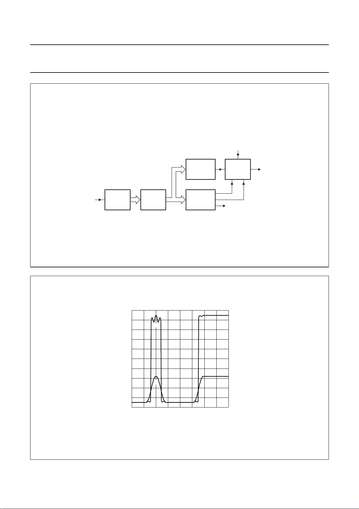
Philips Semiconductors Preliminary specification
YUV one chip picture improvement based on luminance
vector-, colour vector- and spectral processor
handbook, full pagewidth
MINMAX
SELECTOR
Y
in
DELAY
CLAMPS
MINMAX
line width
control
FADER
Y
envelope
Y
MGR905
TDA9178
step
(1) 90% of nominal amplitude.
(2) 30% of nominal amplitude.
Fig.11 Block diagram of the step improvement processor.
1000
handbook, halfpage
V
o
(mV)
800
600
400
200
0
0 0.5
(1)
(2)
1.0 1.5 2.0
MGR906
t (µs)
Fig.12 Response signals for maximum step improvement, no peaking and nominal line width.
1999 Sep 24 26
Page 27
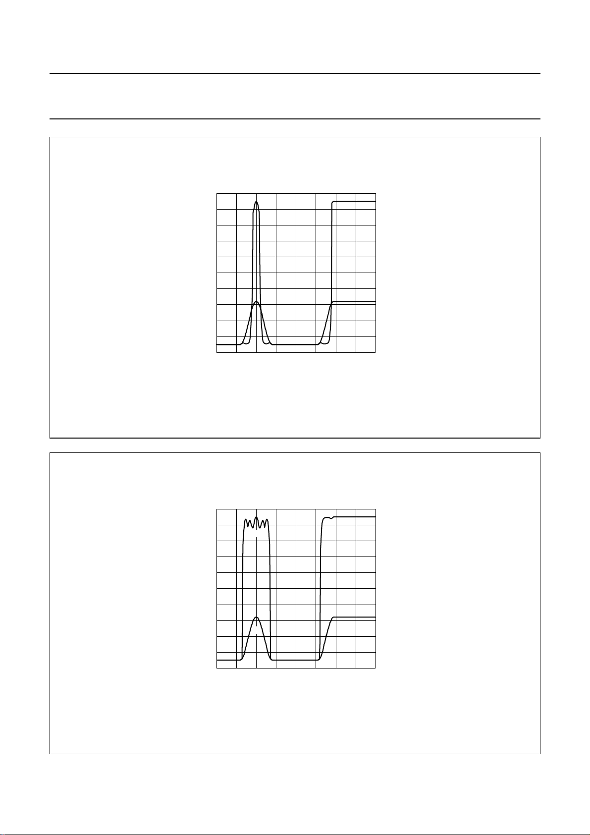
Philips Semiconductors Preliminary specification
YUV one chip picture improvement based on luminance
vector-, colour vector- and spectral processor
1000
handbook, halfpage
V
o
(mV)
800
600
400
200
0
0 0.5
(1)
(2)
1.0 1.5 2.0
MGR907
t (µs)
TDA9178
(1) 90% of nominal amplitude.
(2) 30% of nominal amplitude.
Fig.13 Response signals for maximum step improvement, no peaking and minimum line width.
1000
handbook, halfpage
V
o
(mV)
800
600
400
200
0
0 0.5
MGR908
(1)
(2)
1.0 1.5 2.0
t (µs)
(1) 90% of nominal amplitude.
(2) 30% of nominal amplitude.
Fig.14 Response signals for maximum step improvement, no peaking and maximum line width.
1999 Sep 24 27
Page 28
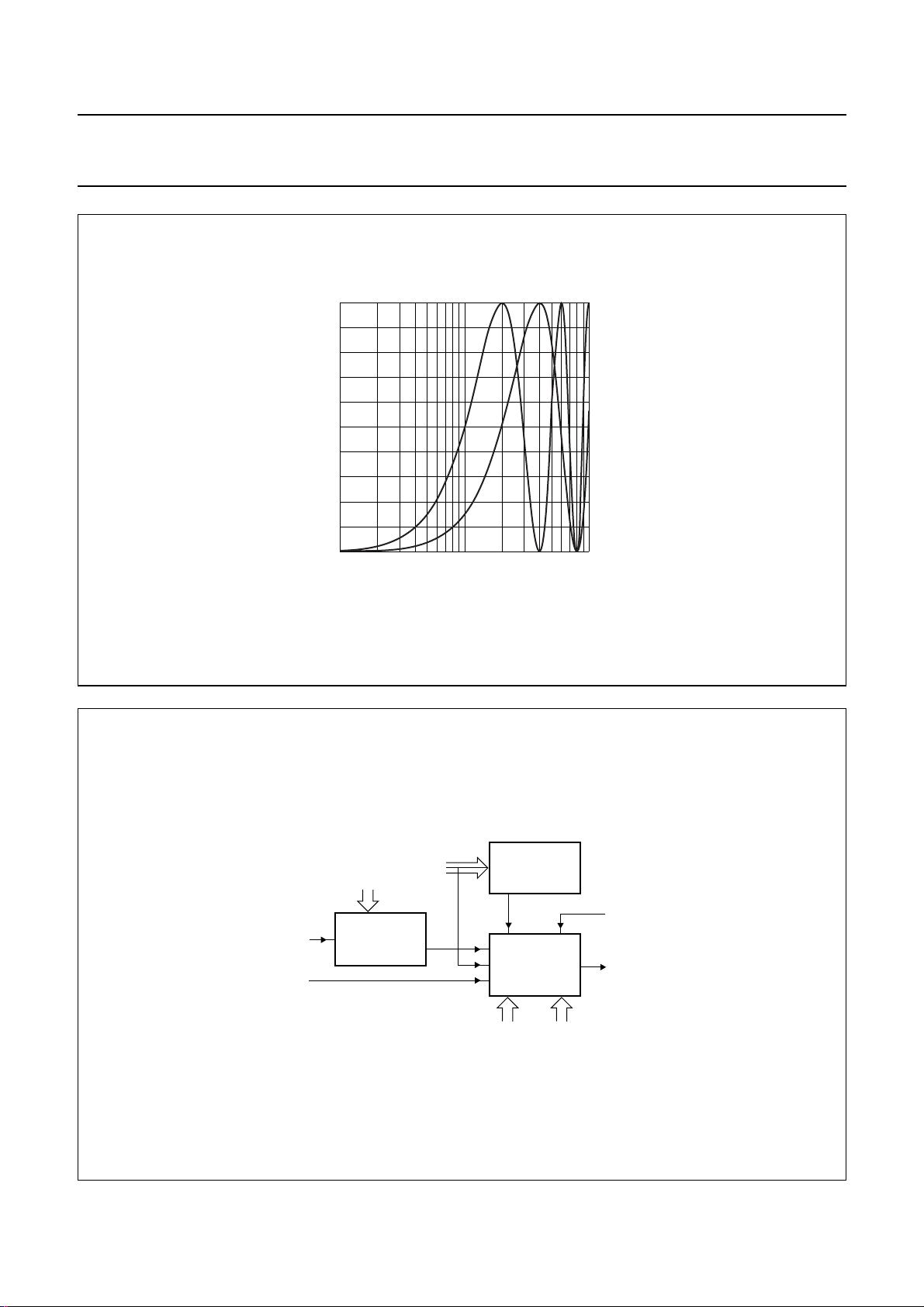
Philips Semiconductors Preliminary specification
YUV one chip picture improvement based on luminance
vector-, colour vector- and spectral processor
f (Hz)
MGR909
7
10
100
handbook, halfpage
contour
(%)
80
60
40
20
0
5
10
(1)
(2)
6
10
TDA9178
(1) 1fHmode.
(2) 2fHmode.
handbook, full pagewidth
Fig.15 Frequency transfers of contour filter at f = 2.0 MHz.
DETECTOR
FADER
peaking
control
STEP
steepness
control
Y
envelope
Y
step
MGR910
Y
contour
Y
step
coring
control
CORING
delay
cells
Y
c
Fig.16 Block diagram of smart sharpness controller.
1999 Sep 24 28
Page 29
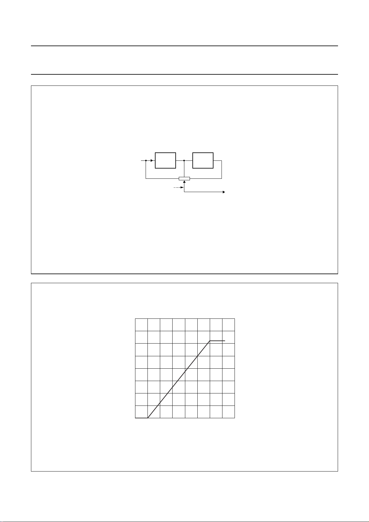
Philips Semiconductors Preliminary specification
YUV one chip picture improvement based on luminance
vector-, colour vector- and spectral processor
handbook, halfpage
UV
in
DELAY DELAY
B
AC
control
MGR911
UV
out
TDA9178
Fig.17 Block diagram of colour transient improvement.
−20
MGR912
S/N (dB)
80
handbook, halfpage
DACvalue
60
40
20
0
−50 −40 −30 −10
Fig.18 Typical noise measurement curve of input noise (dB) versus DAC-value.
1999 Sep 24 29
Page 30
Philips Semiconductors Preliminary specification
YUV one chip picture improvement based on luminance
TDA9178
vector-, colour vector- and spectral processor
TEST AND APPLICATION INFORMATION
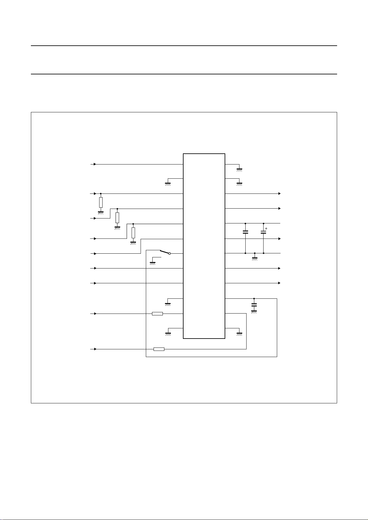
The TDA9178 is especially designed for YUV applications. A typical application diagram is shown in Fig.19.
handbook, full pagewidth
sandcastle
ADEXT1
ADEXT2
ADEXT3
YIN
UIN
100 kΩ
100 kΩ
100 kΩ
ADEXT1
ADEXT2
ADEXT3
1
0
SC
1
n.c.
223
3
4
5
YIN
6
ADR
UIN
TDA9178
7
8
24
22
21
20
19
18
17
n.c.
n.c.
CF
SOUT
V
CC
YOUT
V
EE
UOUT
100
nF
10
µF
CF
SOUT
8 V
YOUT
0 V
UOUT
VIN
SCL
SDA
VIN
9
TP
10 15
100 Ω
100 Ω
SCL
11
n.c.
12 13
Fig.19 YUV application.
VOUT
16
DEC
DIG
SDA
14
n.c.
100 nF
VOUT
MGR913
1999 Sep 24 30
Page 31
Philips Semiconductors Preliminary specification
YUV one chip picture improvement based on luminance
vector-, colour vector- and spectral processor
PACKAGE OUTLINES
SDIP24: plastic shrink dual in-line package; 24 leads (400 mil)
D
A
2
seating plane
L
Z
24
A
e
b
b
1
13
A
1
w M
TDA9178
SOT234-1
M
E
c
(e )
M
1
H
pin 1 index
1
0 5 10 mm
scale
DIMENSIONS (mm are the original dimensions)
A
A
A
UNIT b
Note
1. Plastic or metal protrusions of 0.25 mm maximum per side are not included.
mm
OUTLINE
VERSION
SOT234-1
max.
4.7 0.51 3.8
12
min.
max.
IEC JEDEC EIAJ
1.3
0.8
b
1
0.53
0.40
REFERENCES
cEe M
0.32
0.23
(1) (1)
D
22.3
21.4
9.1
8.7
E
12
(1)
Z
L
3.2
2.8
EUROPEAN
PROJECTION
M
10.7
10.2
E
12.2
10.5
e
1
w
H
0.181.778 10.16
ISSUE DATE
92-11-17
95-02-04
max.
1.6
1999 Sep 24 31
Page 32
Philips Semiconductors Preliminary specification
YUV one chip picture improvement based on luminance
vector-, colour vector- and spectral processor
SO24: plastic small outline package; 24 leads; body width 7.5 mm
D
c
y
Z
24
13
TDA9178
SOT137-1
E
H
E
A
X
v M
A
pin 1 index
1
e
0 5 10 mm
DIMENSIONS (inch dimensions are derived from the original mm dimensions)
mm
A
max.
2.65
0.10
A1A2A
0.30
2.45
0.10
2.25
0.012
0.096
0.004
0.089
0.25
0.01
b
3
p
0.49
0.32
0.36
0.23
0.019
0.013
0.014
0.009
UNIT
inches
Note
1. Plastic or metal protrusions of 0.15 mm maximum per side are not included.
(1)E(1) (1)
cD
15.6
15.2
0.61
0.60
12
w M
b
p
scale
eHELLpQ
7.6
1.27
7.4
0.30
0.050
0.29
10.65
10.00
0.419
0.394
A
1.4
0.055
Q
2
A
1
detail X
1.1
1.1
0.4
0.043
0.016
1.0
0.043
0.039
0.25
0.01
L
p
L
(A )
0.25 0.1
0.01
A
3
θ
ywv θ
Z
0.9
0.4
0.035
0.004
0.016
o
8
o
0
OUTLINE
VERSION
SOT137-1
IEC JEDEC EIAJ
075E05 MS-013AD
REFERENCES
1999 Sep 24 32
EUROPEAN
PROJECTION
ISSUE DATE
95-01-24
97-05-22
Page 33

Philips Semiconductors Preliminary specification
YUV one chip picture improvement based on luminance
vector-, colour vector- and spectral processor
SOLDERING
Introduction
Thistextgivesaverybriefinsighttoa complex technology.
A more in-depth account of soldering ICs can be found in
our
“Data Handbook IC26; Integrated Circuit Packages”
(document order number 9398 652 90011).
There is no soldering method that is ideal for all IC
packages. Wave soldering is often preferred when
through-holeandsurfacemountcomponentsaremixedon
one printed-circuit board. However, wave soldering is not
always suitable for surface mount ICs, or for printed-circuit
boards with high population densities. In these situations
reflow soldering is often used.
Through-hole mount packages
SOLDERING BY DIPPING OR BY SOLDER WAVE
The maximum permissible temperature of the solder is
260 °C; solder at this temperature must not be in contact
with the joints for more than 5 seconds. The total contact
time of successive solder waves must not exceed
5 seconds.
The device may be mounted up to the seating plane, but
the temperature of the plastic body must not exceed the
specified maximum storage temperature (T
printed-circuit board has been pre-heated, forced cooling
may be necessary immediately after soldering to keep the
temperature within the permissible limit.
MANUAL SOLDERING
Apply the soldering iron (24 V or less) to the lead(s) of the
package, either below the seating plane or not more than
2 mm above it. If the temperature of the soldering iron bit
is less than 300 °C it may remain in contact for up to
10 seconds. If the bit temperature is between
300 and 400 °C, contact may be up to 5 seconds.
Surface mount packages
REFLOW SOLDERING
Reflow soldering requires solder paste (a suspension of
fine solder particles, flux and binding agent) to be applied
totheprinted-circuit board by screen printing, stencilling or
pressure-syringe dispensing before package placement.
Several methods exist for reflowing; for example,
infrared/convection heating in a conveyor type oven.
Throughput times (preheating, soldering and cooling) vary
between 100 and 200 seconds depending on heating
method.
stg(max)
). If the
Typical reflow peak temperatures range from
215 to 250 °C. The top-surface temperature of the
packages should preferable be kept below 230 °C.
WAVE SOLDERING
Conventional single wave soldering is not recommended
forsurfacemountdevices(SMDs)orprinted-circuitboards
with a high component density, as solder bridging and
non-wetting can present major problems.
To overcome these problems the double-wave soldering
method was specifically developed.
If wave soldering is used the following conditions must be
observed for optimal results:
• Use a double-wave soldering method comprising a
turbulent wave with high upward pressure followed by a
smooth laminar wave.
• For packages with leads on two sides and a pitch (e):
– larger than or equal to 1.27 mm, the footprint
longitudinal axis is preferred to be parallel to the
transport direction of the printed-circuit board;
– smaller than 1.27 mm, the footprint longitudinal axis
must be parallel to the transport direction of the
printed-circuit board.
The footprint must incorporate solder thieves at the
downstream end.
• Forpackageswithleadsonfoursides,thefootprintmust
be placed at a 45° angle to the transport direction of the
printed-circuit board. The footprint must incorporate
solder thieves downstream and at the side corners.
During placement and before soldering, the package must
be fixed with a droplet of adhesive. The adhesive can be
applied by screen printing, pin transfer or syringe
dispensing. The package can be soldered after the
adhesive is cured.
Typical dwell time is 4 seconds at 250 °C.
A mildly-activated flux will eliminate the need for removal
of corrosive residues in most applications.
MANUAL SOLDERING
Fix the component by first soldering two
diagonally-opposite end leads. Use a low voltage (24 V or
less) soldering iron applied to the flat part of the lead.
Contact time must be limited to 10 seconds at up to
300 °C.
When using a dedicated tool, all other leads can be
soldered in one operation within 2 to 5 seconds between
270 and 320 °C.
TDA9178
1999 Sep 24 33
Page 34

Philips Semiconductors Preliminary specification
YUV one chip picture improvement based on luminance
TDA9178
vector-, colour vector- and spectral processor
Suitability of IC packages for wave, reflow and dipping soldering methods
MOUNTING PACKAGE
Through-hole mount DBS, DIP, HDIP, SDIP, SIL suitable
Surface mount BGA, LFBGA, SQFP, TFBGA not suitable suitable −
HBCC, HLQFP, HSQFP, HSOP, HTQFP,
HTSSOP, SMS
(4)
PLCC
LQFP, QFP, TQFP not recommended
SSOP, TSSOP, VSO not recommended
Notes
1. All surface mount (SMD) packages are moisture sensitive. Depending upon the moisture content, the maximum
temperature (with respect to time) and body size of the package, there is a risk that internal or external package
cracks may occur due to vaporization of the moisture in them (the so called popcorn effect). For details, refer to the
Drypack information in the
2. For SDIP packages, the longitudinal axis must be parallel to the transport direction of the printed-circuit board.
3. These packages are not suitable for wave soldering as a solder joint between the printed-circuit board and heatsink
(at bottom version) can not be achieved, and as solder may stick to the heatsink (on top version).
4. If wave soldering is considered, then the package must be placed at a 45° angle to the solder wave direction.
The package footprint must incorporate solder thieves downstream and at the side corners.
5. Wave soldering is only suitable for LQFP, QFP and TQFP packages with a pitch (e) equal to or larger than 0.8 mm;
it is definitely not suitable for packages with a pitch (e) equal to or smaller than 0.65 mm.
6. Wave soldering is only suitable for SSOP and TSSOP packages with a pitch (e) equal to or larger than 0.65 mm; it is
definitely not suitable for packages with a pitch (e) equal to or smaller than 0.5 mm.
, SO, SOJ suitable suitable −
“Data Handbook IC26; Integrated Circuit Packages; Section: Packing Methods”
not suitable
SOLDERING METHOD
WAVE REFLOW
(2)
(3)
− suitable
suitable −
(4)(5)
suitable −
(6)
suitable −
(1)
DIPPING
.
1999 Sep 24 34
Page 35

Philips Semiconductors Preliminary specification
YUV one chip picture improvement based on luminance
TDA9178
vector-, colour vector- and spectral processor
DEFINITIONS
Data sheet status
Objective specification This data sheet contains target or goal specifications for product development.
Preliminary specification This data sheet contains preliminary data; supplementary data may be published later.
Product specification This data sheet contains final product specifications.
Limiting values
Limiting values given are in accordance with the Absolute Maximum Rating System (IEC 134). Stress above one or
more of the limiting values may cause permanent damage to the device. These are stress ratings only and operation
of the device at these or at any other conditions above those given in the Characteristics sections of the specification
is not implied. Exposure to limiting values for extended periods may affect device reliability.
Application information
Where application information is given, it is advisory and does not form part of the specification.
LIFE SUPPORT APPLICATIONS
These products are not designed for use in life support appliances, devices, or systems where malfunction of these
products can reasonably be expected to result in personal injury. Philips customers using or selling these products for
use in such applications do so at their own risk and agree to fully indemnify Philips for any damages resulting from such
improper use or sale.
PURCHASE OF PHILIPS I
Purchase of Philips I
components in the I2C system provided the system conforms to the I2C specification defined by
Philips. This specification can be ordered using the code 9398 393 40011.
2
C COMPONENTS
2
C components conveys a license under the Philips’ I2C patent to use the
1999 Sep 24 35
Page 36

Philips Semiconductors – a w orldwide compan y
Argentina: see South America
Australia: 3 Figtree Drive, HOMEBUSH, NSW 2140,
Tel. +61 2 9704 8141, Fax. +61 2 9704 8139
Austria: Computerstr. 6, A-1101 WIEN, P.O. Box 213,
Tel. +43 1 60 101 1248, Fax. +43 1 60 101 1210
Belarus: Hotel Minsk Business Center, Bld. 3, r. 1211, Volodarski Str. 6,
220050 MINSK, Tel. +375 172 20 0733, Fax. +375 172 20 0773
Belgium: see The Netherlands
Brazil: see South America
Bulgaria: Philips Bulgaria Ltd., Energoproject, 15th floor,
51 James Bourchier Blvd., 1407 SOFIA,
Tel. +359 2 68 9211, Fax. +359 2 68 9102
Canada: PHILIPS SEMICONDUCTORS/COMPONENTS,
Tel. +1 800 234 7381, Fax. +1 800 943 0087
China/Hong Kong: 501 Hong Kong Industrial Technology Centre,
72 Tat Chee Avenue, Kowloon Tong, HONG KONG,
Tel. +852 2319 7888, Fax. +852 2319 7700
Colombia: see South America
Czech Republic: see Austria
Denmark: Sydhavnsgade 23, 1780 COPENHAGEN V,
Tel. +45 33 29 3333, Fax. +45 33 29 3905
Finland: Sinikalliontie 3, FIN-02630 ESPOO,
Tel. +358 9 615 800, Fax. +358 9 6158 0920
France: 51 Rue Carnot, BP317, 92156 SURESNES Cedex,
Tel. +33 1 4099 6161, Fax. +33 1 4099 6427
Germany: Hammerbrookstraße 69, D-20097 HAMBURG,
Tel. +49 40 2353 60, Fax. +49 40 2353 6300
Hungary: see Austria
India: Philips INDIA Ltd, Band Box Building, 2nd floor,
254-D, Dr. Annie Besant Road, Worli, MUMBAI 400 025,
Tel. +91 22 493 8541, Fax. +91 22 493 0966
Indonesia: PTPhilips DevelopmentCorporation,Semiconductors Division,
Gedung Philips, Jl. Buncit Raya Kav.99-100, JAKARTA 12510,
Tel. +62 21 794 0040 ext. 2501, Fax. +62 21 794 0080
Ireland: Newstead, Clonskeagh, DUBLIN 14,
Tel. +353 1 7640 000, Fax. +353 1 7640 200
Israel: RAPAC Electronics, 7 Kehilat Saloniki St, PO Box 18053,
TEL AVIV 61180, Tel. +972 3 645 0444, Fax. +972 3 649 1007
Italy: PHILIPS SEMICONDUCTORS,ViaCasati,23 - 20052 MONZA (MI),
Tel. +39 039 203 6838, Fax +39 039 203 6800
Japan: Philips Bldg 13-37, Kohnan 2-chome, Minato-ku,
TOKYO 108-8507, Tel. +81 3 3740 5130, Fax. +81 3 3740 5057
Korea: Philips House, 260-199 Itaewon-dong, Yongsan-ku, SEOUL,
Tel. +82 2 709 1412, Fax. +82 2 709 1415
Malaysia: No. 76 Jalan Universiti, 46200 PETALING JAYA, SELANGOR,
Tel. +60 3 750 5214, Fax. +60 3 757 4880
Mexico: 5900 Gateway East, Suite 200, EL PASO, TEXAS 79905,
Tel. +9-5 800 234 7381, Fax +9-5 800 943 0087
Middle East: see Italy
Netherlands: Postbus 90050, 5600 PB EINDHOVEN, Bldg. VB,
Tel. +31 40 27 82785, Fax. +31 40 27 88399
New Zealand: 2 Wagener Place, C.P.O. Box 1041, AUCKLAND,
Tel. +64 9 849 4160, Fax. +64 9 849 7811
Norway: Box 1, Manglerud 0612, OSLO,
Tel. +47 22 74 8000, Fax. +47 22 74 8341
Pakistan: see Singapore
Philippines: Philips Semiconductors Philippines Inc.,
106 Valero St. Salcedo Village, P.O. Box 2108 MCC, MAKATI,
Metro MANILA, Tel. +63 2 816 6380, Fax. +63 2 817 3474
Poland: Al.Jerozolimskie 195 B, 02-222 WARSAW,
Tel. +48 22 5710 000, Fax. +48 22 5710 001
Portugal: see Spain
Romania: see Italy
Russia: Philips Russia, Ul. Usatcheva 35A, 119048 MOSCOW,
Tel. +7 095 755 6918, Fax. +7 095 755 6919
Singapore: Lorong 1, Toa Payoh, SINGAPORE 319762,
Tel. +65 350 2538, Fax. +65 251 6500
Slovakia: see Austria
Slovenia: see Italy
South Africa: S.A. PHILIPS Pty Ltd., 195-215 Main Road Martindale,
2092 JOHANNESBURG, P.O. Box 58088 Newville 2114,
Tel. +27 11 471 5401, Fax. +27 11 471 5398
South America: Al. Vicente Pinzon, 173, 6th floor,
04547-130 SÃO PAULO, SP, Brazil,
Tel. +55 11 821 2333, Fax. +55 11 821 2382
Spain: Balmes 22, 08007 BARCELONA,
Tel. +34 93 301 6312, Fax. +34 93 301 4107
Sweden: Kottbygatan 7, Akalla, S-16485 STOCKHOLM,
Tel. +46 8 5985 2000, Fax. +46 8 5985 2745
Switzerland: Allmendstrasse 140, CH-8027 ZÜRICH,
Tel. +41 1 488 2741 Fax. +41 1 488 3263
Taiwan: Philips Semiconductors, 6F, No. 96, Chien Kuo N. Rd., Sec. 1,
TAIPEI, Taiwan Tel. +886 2 2134 2886, Fax. +886 2 2134 2874
Thailand: PHILIPS ELECTRONICS (THAILAND) Ltd.,
209/2 Sanpavuth-Bangna Road Prakanong, BANGKOK 10260,
Tel. +66 2 745 4090, Fax. +66 2 398 0793
Turkey: Yukari Dudullu, Org. San. Blg., 2.Cad. Nr. 28 81260 Umraniye,
ISTANBUL, Tel. +90 216 522 1500, Fax. +90 216 522 1813
Ukraine: PHILIPS UKRAINE, 4 Patrice Lumumba str., Building B, Floor 7,
252042 KIEV, Tel. +380 44 264 2776, Fax. +380 44 268 0461
United Kingdom: Philips Semiconductors Ltd., 276 Bath Road, Hayes,
MIDDLESEX UB3 5BX, Tel. +44 208 730 5000, Fax. +44 208 754 8421
United States: 811 East Arques Avenue, SUNNYVALE, CA 94088-3409,
Tel. +1 800 234 7381, Fax. +1 800 943 0087
Uruguay: see South America
Vietnam: see Singapore
Yugoslavia: PHILIPS, Trg N. Pasica 5/v, 11000 BEOGRAD,
Tel. +381 11 62 5344, Fax.+381 11 63 5777
For all other countries apply to: Philips Semiconductors,
International Marketing & Sales Communications, Building BE-p, P.O. Box 218,
5600 MD EINDHOVEN, The Netherlands, Fax. +31 40 27 24825
© Philips Electronics N.V. SCA
All rights are reserved. Reproduction in whole or in part is prohibited without the prior written consent of the copyright owner.
The information presented in this document does not form part of any quotation or contract, is believed to be accurate and reliable and may be changed
without notice. No liability will be accepted by the publisher for any consequence of its use. Publication thereof does not convey nor imply any license
under patent- or other industrial or intellectual property rights.
1999
Internet: http://www.semiconductors.philips.com
68
Printed in The Netherlands 545004/01/pp36 Date of release: 1999 Sep 24 Document order number: 9397 750 04621
Page 37

This datasheet has been download from:
www.datasheetcatalog.com
Datasheets for electronics components.
 Loading...