

Page 1

INTEGRATED CIRCUITS
DATA SH EET
TDA9141
PAL/NTSC/SECAM decoder/sync
processor
Product specification
File under Integrated Circuits, IC02
December 1992
Page 2
Philips Semiconductors Product specification
PAL/NTSC/SECAM decoder/sync processor TDA9141
FEATURES
• Multistandard PAL, NTSC and SECAM
• I2C-bus controlled
• I2C-bus addresses can be selected by hardware
• Alignment free
• Few external components
• Designed for use with baseband delay lines
• Integrated video filters
• CVBS or YC input with automatic detection
• CVBS output
• Vertical divider system
• Two-level sandcastle signal
• VA synchronization pulse (3-state)
• HA synchronization pulse or clamping pulse CLP
input/output
• Line-locked clock output or stand-alone I2C-bus output
port
• Stand-alone I2C-bus input/output port
• Colour matrix and fast YUV switch
• Comb filter enable input/output with subcarrier
frequency.
GENERAL DESCRIPTION
The TDA9141 is an I2C-bus controlled, alignment-free
PAL/NTSC/SECAM decoder/sync processor. The
TDA9141 has been designed for use with baseband
chrominance delay lines, and has a combined subcarrier
frequency/comb filter enable signal for communication
with a PAL comb filter.
The IC can process CVBS signals and Y/C input signals.
The input signal is available on an output pin, in the event
of a Y/C signal, it is added into a CVBS signal.
The sync processor provides a two-level sandcastle, a
horizontal pulse (CLP or HA pulse, bus selectable) and a
vertical (VA) pulse. When the HA pulse is selected a
line-locked clock (LLC) signal is available at the output port
pin.
A fast switch can select either the internal Y signal with the
UV input signals, or YUV signals made of the RGB input
signals. The RGB input signals can be clamped with either
the internal or an external clamping signal (search tuning
mode).
Two pins with an input/output port and an output port of the
I2C-bus are available.
The I2C-bus address of the TDA9141 is hardware
programmable.
ORDERING INFORMATION
EXTENDED TYPE
NUMBER
TDA9141 32 SDIL plastic SOT232
Note
1. SOT232-1; 1996 December 4.
December 1992 2
PINS PIN POSITION MATERIAL CODE
PACKAGE
(1)
Page 3
Philips Semiconductors Product specification
PAL/NTSC/SECAM decoder/sync
processor
TDA9141
December 1992 3
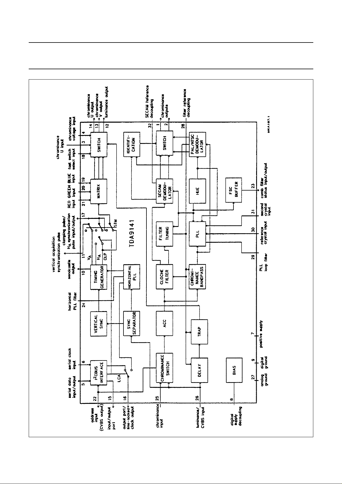
Fig.1 Block diagram.
Page 4
Philips Semiconductors Product specification
PAL/NTSC/SECAM decoder/sync processor TDA9141
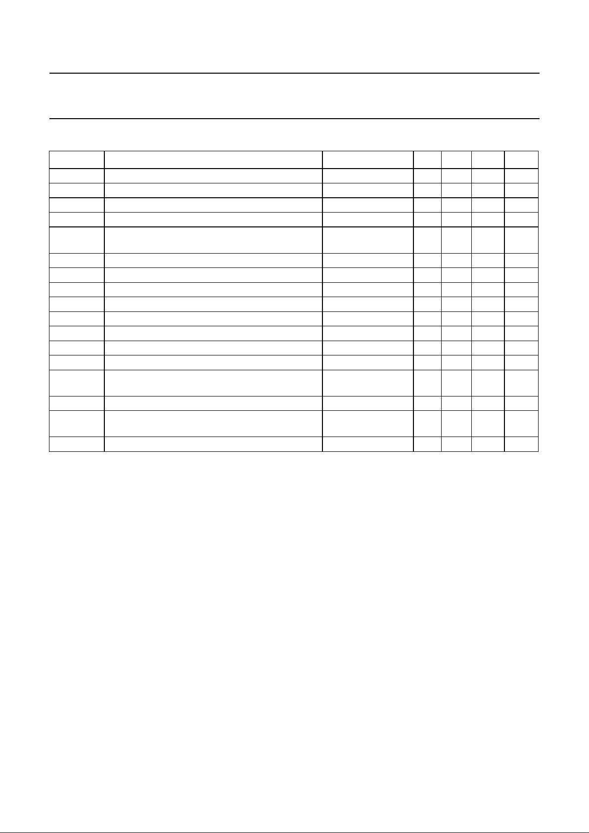
QUICK REFERENCE DATA
SYMBOL PARAMETER CONDITIONS MIN. TYP. MAX. UNIT
V
CC
I
CC
V
26(p-p)
V
26(p-p)
V
22(p-p)
V
12
V
14(p-p)
V
13(p-p)
V
10
V
10
V
11
V
17
V
16(p-p)
V
21,20 19(p-p)
V
clamp I/O
V
sub
V
15,16
positive supply voltage 7.2 8.0 8.8 V
supply current − 45 − mA
CVBS input voltage (peak-to-peak value) top sync - white − 1.0 − V
luminance input voltage (peak-to-peak value) top sync - white − 1.0 − V
chrominance burst input voltage (peak-to-peak
− 0.3 − V
value)
luminance black-white output voltage − 1.0 − V
U output voltage (peak-to-peak value) standard colour bar − 1.33 − V
V output voltage (peak-to-peak value) standard colour bar − 1.05 − V
sandcastle blanking voltage level − 2.5 − V
sandcastle clamping voltage level − 4.5 − V
VA output voltage − 5.0 − V
HA output voltage − 5.0 − V
LLC output voltage amplitude (peak-to-peak value) − 500 − mV
RGB input voltage (peak-to-peak value) 0 to 100%
− 0.7 − V
saturation
clamping pulse input/output voltage − 5.0 − V
subcarrier output voltage amplitude
− 200 − mV
(peak-to-peak value)
O port output voltage − 5.0 − V
December 1992 4
Page 5
Philips Semiconductors Product specification
PAL/NTSC/SECAM decoder/sync processor TDA9141
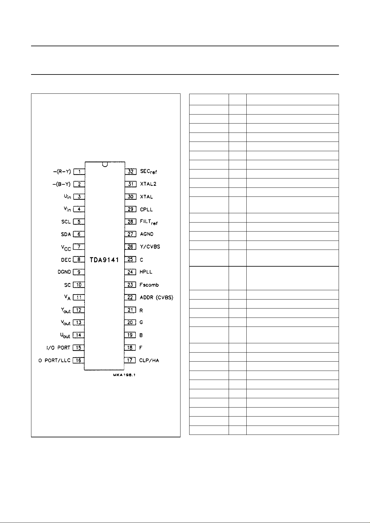
PINNING
SYMBOL PIN DESCRIPTION
−(R−Y) 1 chrominance output
−(B−Y) 2 chrominance output
3 chrominance U input
4 chrominance voltage input
7 positive supply input
11 vertical acquisition
synchronization pulse
12 luminance output
13 chrominance V output
14 chrominance U output
output
A
synchronization pulse
input/output
22 I
2
C-bus address input (CVBS
output)
28 filter reference decoupling
32 SECAM reference decoupling
Fig.2 Pin configuration.
U
in
V
in
SCL 5 serial clock input
SDA 6 serial data input/output
V
CC
DEC 8 digital supply decoupling
DGND 9 digital ground
SC 10 sandcastle output
V
A
Y
out
V
out
U
out
I/O PORT 15 input/output port
O PORT/LLC 16 output port/line-locked clock
CLP/HA 17 clamping pulse/H
F 18 fast switch select input
B 19 BLUE input
G 20 GREEN input
R 21 RED input
ADDR
(CVBS)
Fscomb 23 comb filter status input/output
HPLL 24 horizontal PLL filter
C 25 chrominance input
Y/CVBS 26 luminance/CVBS input
AGND 27 analog ground
FILT
ref
CPLL 29 colour PLL filter
XTAL 30 reference crystal input
XTAL2 31 second crystal input
SEC
ref
December 1992 5
Page 6

Philips Semiconductors Product specification
PAL/NTSC/SECAM decoder/sync
processor
FUNCTIONAL DESCRIPTION
General
2
The TDA9141 is an I
C-bus
controlled, alignment-free
PAL/NTSC/SECAM colour
decoder/sync processor which has
been designed for use with baseband
chrominance delay lines.
In the standard operating mode the
I2C-bus address is 8A. If the address
input is connected to the positive rail
the address will change to 8E.
Input switch
WARNING: T
CHROMINANCE PIN MUST NEVER
EXCEED
ENTERS A TEST MODE.
HE VOLTAGE ON THE
5.5 V. IF IT DOES THE IC
The TDA9141 has a two pin input for
CVBS or YC signals which can be
selected via the I2C-bus. The input
selector also has a position in which it
automatically detects whether a
CVBS or YC signal is on the input. In
this input selector position, standard
identification first takes place on an
added Y/CVBS and C input signal.
After that, both chrominance signal
input amplitudes are checked once
and the input with the strongest
chrominance burst signal is selected.
The input switch status is read out by
the I2C-bus via output bit YC.
CVBS output
In the standard operating mode with
2
the I
C-bus address 8A, a CVBS
output signal is available on the
address pin, which represents either
the CVBS input signal or the Y/C input
signal, added into a CVBS signal
RGB colour matrix
WARNING: THE VOLTAGE ON THE UIN
PIN MUST NEVER EXCEED
DOES THE
IC ENTERS A TEST MODE.
5.5 V. IFIT
The TDA9141 has a colour matrix to
convert RGB input signals into YUV
signals. A fast switch, controlled by
the signal on pin F and enabled by the
2
C-bus via EFS (enable fast switch),
I
can select between these YUV
signals and the YUV signals of the
decoder. The Y signal is internally
connected to the switch. The −(R−Y)
and −(B−Y) output signals of the
decoder have to first be delayed in
external baseband chrominance
delay lines. The outputs of the delay
lines must be connected to the UV
input pins. If the RGB signals are not
synchronous with the selected
decoder input signal, clamping of the
RGB input signals is possible by
2
C-bus selection of STM (search
I
tuning mode), EFS and by feeding an
external clamping signal to the CLP
pin.
Also in search tuning mode the VA
output will be in a high impedance
OFF-state.
Standard identification
The standards which the TDA9141
can decode are dependent on the
choice of external crystals. If a
4.4 MHz and a 3.6 MHz crystal are
used then SECAM, PAL 4.4/3.6 and
NTSC 4.4/3.6 can be decoded. If two
3.6 MHz crystals are used then only
PAL 3.6 and NTSC 3.6 can be
decoded. Which 3.6 MHz standards
can be decoded is dependent on the
exact frequencies of the 3.6 MHz
crystals. In an application where not
all standards are required only one
crystal is sufficient (in this instance
the crystal must be connected to the
reference crystal input (pin 30)). If a
4.4 MHz crystal is used it must always
be connected to pin 30. Both crystals
are used to provide a reference for
the filters and the horizontal PLL,
however, only the reference crystal is
used to provide a reference for the
SECAM demodulator.
To enable the calibrating circuits to be
adjusted exactly two bits from I
subaddress 00 are used to indicate
which crystals are connected to the
IC.
2
C-bus
TDA9141
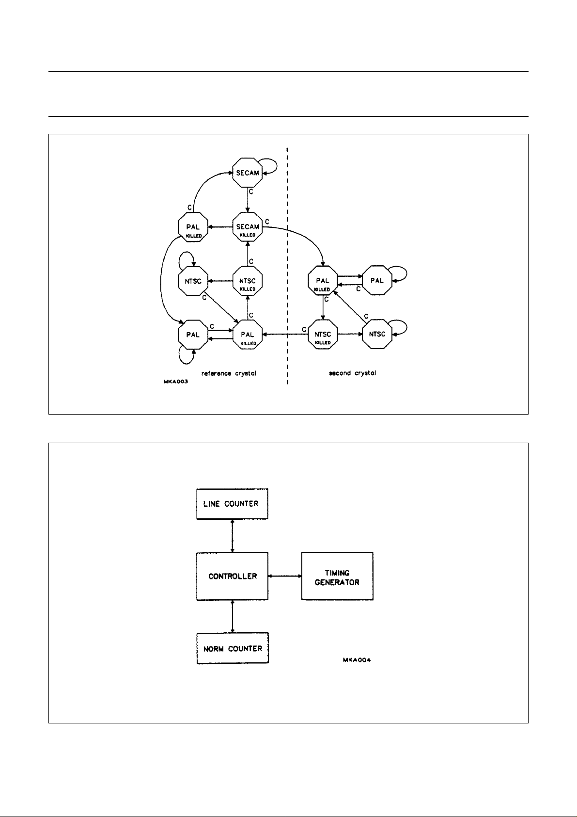
The standard identification circuit is a
digital circuit without external
components; the search loop is
illustrated in Fig.3.
2
The decoder (via the I
forced to decode either SECAM or
PAL/NTSC (but not PAL or NTSC).
Crystal selection can also be forced.
Information concerning which
standard and which crystal have been
selected and whether the colour killer
is ON or OFF is provided by the read
out. Using the forced-mode does not
affect the search loop, it does,
however, prevent the decoder from
reaching or staying in an unwanted
state. The identification circuit skips
impossible standards (e.g. SECAM
when no 4.4 MHz crystal is fitted) and
illegal standards (e.g. is forced
mode). To reduce the risk of wrong
identification PAL has priority over
SECAM (only line identification is
used for SECAM).
Integrated filters
All filters, including the luminance
delay line, are an integral part of the
IC. The filters are gyrator-capacitor
type filters. The resonant frequency of
the filters is controlled by a circuit that
uses the active crystal to tune the
SECAM Cloche filter during the
vertical flyback time. The remaining
filters and the luminance delay line
are matched to this filter. The filters
can be switched to either 4.43 MHz,
4.28 MHz or 3.58 MHz irrespective of
the frequency of the active crystal.
The switching is controlled by the
identification circuit.
In YC mode the chrominance notch
filter is bypassed, to preserve full
signal bandwidth.
For a CVBS signal the chrominance
notch filter can be bypassed by
2
I
C-bus selection of TB (trap bypass).
The luminance delay line delivers the
Y signal to the output 60 ns after the
−(R−Y) and −(B−Y) signals have
arrived at their outputs.
C-bus) can be
December 1992 6
Page 7

Philips Semiconductors Product specification
PAL/NTSC/SECAM decoder/sync
processor
This compensates for the delay of the
external chrominance delay lines.
Colour decoder
The PAL/NTSC demodulator
employs an oscillator that can operate
with either crystal (3.6 or 4.4 MHz). If
2
C-bus indicates that only one
the I
crystal is connected it will always
connect to the crystal on the
reference crystal input (pin 30).
The Hue signal, which is adjustable
via the I2C-bus, is gated during the
burst for NTSC signals.
The SECAM demodulator is an
auto-calibrating PLL demodulator
which has two references. The
reference crystal, to force the PLL to
the desired free-running frequency
and the bandgap reference, to obtain
the correct absolute value of the
output signal. The VCO of the PLL is
calibrated during each vertical
blanking period, when the IC is in
search mode or SECAM mode. If the
reference crystal is not 4.4 MHz the
decoder will not produce the correct
SECAM signals.
The frequency of the active crystal is
fed to the Fscomb output, which can
be connected to an external comb
filter IC. The DC value on this pin
contains the comb enable
information. Comb enable is true
when bus bit ECMB is HIGH. If ECMB
is LOW, the subcarrier frequency is
suppressed. The external comb filter
can force the DC value of Fscomb
LOW, as pin Fscomb also acts as
input pin. In this event the subcarrier
frequency is still present. If the DC
value of Fscomb is HIGH, the input
switch is always forced in Y/C mode,
indicated by bus bit YC.
Sync processor (ϕ1 loop)
The main part of the sync circuit is a
432 × fH (6.75 MHz) oscillator the
frequency of which is divided by 432
to lock the Phase 1 loop to the
incoming signal. The time constant of
the loop can be forced by the I2C-bus
(fast or slow). If required the IC can
select the time constant, depending
on the noise content of the input
signal and whether the loop is
phase-locked or not (medium or
slow). The free-running frequency of
the oscillator is determined by a
digital control circuit that is locked to
the active crystal.
When a power-on-reset pulse is
detected the frequency of the
oscillator is switched to a frequency
greater than 6.75 MHz to protect the
horizontal output transistor. The
oscillator frequency is reset to
6.75 MHz when the crystal indication
bits have been loaded into the IC. To
ensure that this procedure does not
fail it is absolutely necessary to send
subaddress 00 before subaddress
01. Subaddress 00 contains the
crystal indication bits and when
subaddress 01 is received the line
oscillator calibration will be initiated
(for the start-up procedure after
power-on reset detection see the
I2C-bus protocol. The calibration is
terminated when the oscillator
frequency reaches 6.75 MHz. The
oscillator is again calibrated when an
out-of-lock condition with the input
signal is detected by the coincidence
detector. Again the calibration will be
terminated when the oscillator
frequency reaches 6.75 MHz.
The Phase 1 loop can be opened
using the I2C-bus. This is to facilitate
On Screen Display (OSD)
information. If there is no input signal
or a very noisy input signal the phase
1 loop can be opened to provide a
stable line frequency and thus a
stable picture.
TDA9141
The sync part also delivers a
two-level sandcastle signal, which
provides a combined horizontal and
vertical blanking signal and a
clamping pulse for the display section
of the TV.
Vertical divider system
The vertical divider system has a fully
integrated vertical sync separator.
The divider can accommodate both
50 and 60 Hz systems; it can either
locate the field frequency
automatically or it can be forced to the
desired system via the I2C-bus. A
block diagram of the vertical divider
system is illustrated in Fig.4. The
divider system operates at twice the
horizontal line frequency. The line
counter receives enable pulses at this
line frequency, thereby counting two
pulses per line.
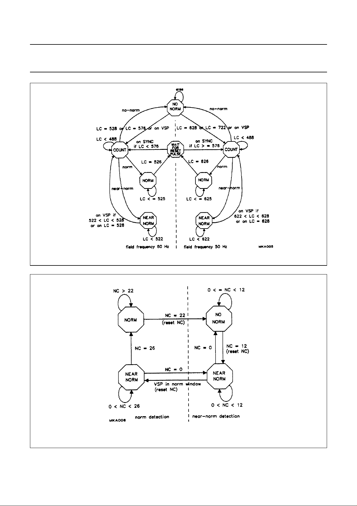
A state diagram of the controller is
illustrated in Fig.5. Because it is
symmetrical only the right hand part
will be described.
Depending on the previously found
field frequency, the controller will be
in one of the COUNT states. When
the line counter has counted 488
pulses (i.e. 244 lines of the video
input signal) the controller will move
to the next state depending on the
output of the norm counter. This can
be either NORM, NEAR_NORM or
NO_NORM depending on the
position of the vertical sync pulse in
the previous fields. When the
controller is in the NORM state it
generates the vertical sync pulse
(VSP) automatically and then, when
the line counter is at LC = 626,
moves to the WAIT state. In this
condition it waits for the next pulse of
the double line frequency signal and
then moves to the COUNT state of
the current field frequency. When the
controller returns to the COUNT state
the line counter will be reset half a line
after the start of the vertical sync
pulse of the video input signal.
December 1992 7
Page 8

Philips Semiconductors Product specification
PAL/NTSC/SECAM decoder/sync
processor
When the controller is in the
NEAR_NORM state it will move to the
COUNT state if it detects the vertical
sync pulse within the NEAR_NORM
window (i.e. 622 < LC < 628). If no
vertical sync pulse is detected, the
controller will move back to the
COUNT state when the line counter
reaches LC = 628. The line counter
will then be reset.
When the controller is in the
NO_NORM state it will move to the
COUNT state when it detects a
vertical sync pulse and reset the line
counter. If a vertical sync pulse is not
detected before LC = 722 (if the
Phase 1 loop is locked in forced
mode) it will move to the COUNT
state and reset the line counter. If the
Phase 1 loop is not locked the
controller will move back to the
COUNT state when LC = 628.
The forced mode option keeps the
controller in either the left-hand side
(60 Hz) or the right-hand side (50 Hz)
of the state diagram.
Figure 6 illustrates the state diagram
of the norm counter which is an
up/down counter that counts up if it
finds a vertical sync pulse within the
selected window. In the
NEAR_NORM and NORM states the
first correct vertical sync pulse after
one or more incorrect vertical sync
pulses is processed as an incorrect
pulse. This procedure prevents the
system from staying in the
NEAR_NORM or NORM state if the
vertical sync pulse is correct in the
first field and incorrect in the second
field. If no vertical sync pulse is found
in the selected window this will always
result in a down pulse for the norm
counter.
TDA9141
Output port and input/output port
Two stand-alone ports are available
for external use. These ports are
2
I
C-bus controlled, the output port by
bus bit OPB and the input/output port
by bus bit OPA. Bus bit OPA is an
open-drain output, to enable input
port functioning. The pin status is
read out by bus via output bit IP.
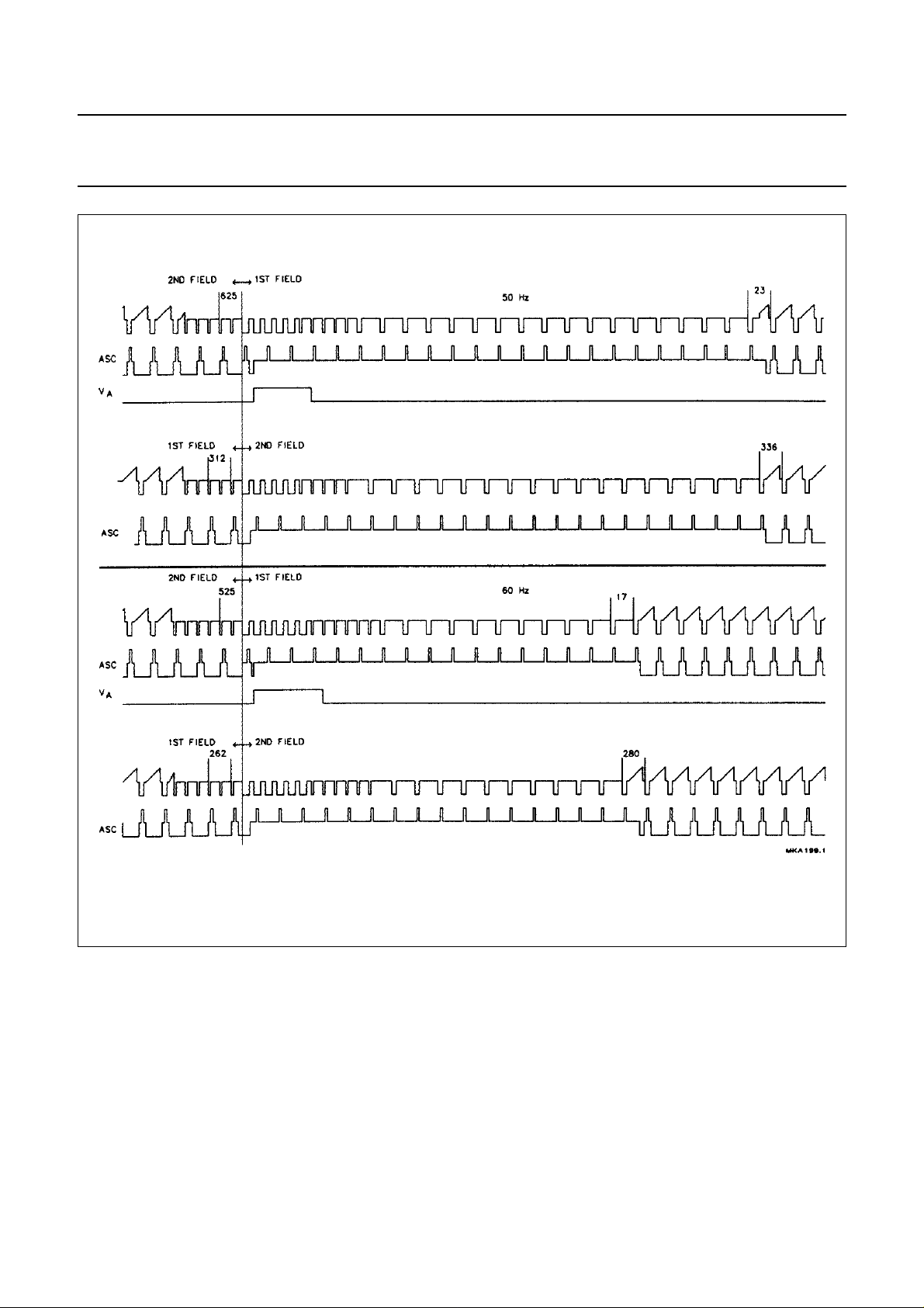
Sandcastle
Figure 7 illustrates the timing of the
acquisition sandcastle (ASC) and the
pulse with respect to the input
V
A
signal. The sandcastle signal is in
accordance with the 2-level 5 V
sandcastle format. An external
vertical guard current can overrule the
sink current to enable blanking
purposes.
December 1992 8
Page 9
Philips Semiconductors Product specification
PAL/NTSC/SECAM decoder/sync
processor
TDA9141
Fig.3 Search loop of the identification circuit.
Fig.4 Block diagram of the vertical divider system.
December 1992 9
Page 10
Philips Semiconductors Product specification
PAL/NTSC/SECAM decoder/sync
processor
TDA9141
Fig.5 State diagram of the vertical divider system.
Fig.6 State diagram of the norm counter.
December 1992 10
Page 11
Philips Semiconductors Product specification
PAL/NTSC/SECAM decoder/sync processor TDA9141
Fig.7 Acquisition sandcastle signal and VA pulse timing diagram.
December 1992 11
Page 12
Philips Semiconductors Product specification
PAL/NTSC/SECAM decoder/sync processor TDA9141
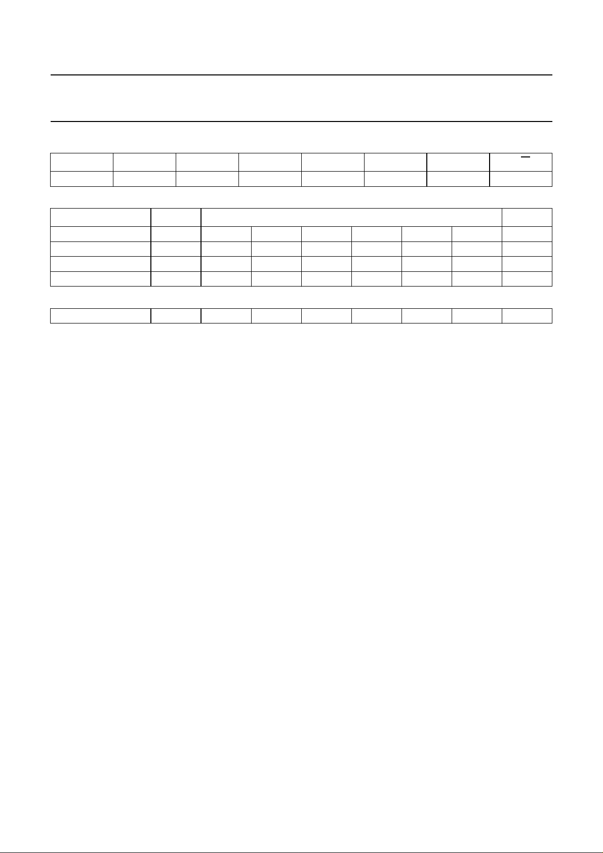
Table 1 Slave address (8A).
A6 A5 A4 A3 A2 A1 A0 R/
10001X1X
Table 2 Inputs.
SUBADDRESS MSB LSB
00 INA INB TB ECMB FOA FOB XA XB
01 FORF FORS OPA OPB POC FM SAF FRQF
02 EFS STM HU5 HU4 HU3 HU2 HU1 HU0
03 LCA −−−−−−−
Table 3 Outputs.
ADDRESS POR FSI YC SL IP SAK SBK FRQ
2
C-bus protocol
I
If the address input is connected to the positive supply the address will change from 8A to 8E.
Valid subaddresses = 00 to 0F
Auto-increment mode available for subaddresses.
Start-up procedure: read the status byte until POR = 0; send subaddress 00 with the crystal indicator bits (XA and XB)
indicating that only one crystal is connected to the IC; wait for 250 ms; send subaddress 01; wait for at least 100 ms; set
XA, XB to the actual crystal configuration.
Each time before the data in the IC is refreshed, the status byte must be read. If POR = 1, then the above procedure
must be carried out to restart the IC.
Failure to stick to the above procedure may result in an incorrect line frequency after power-up or a power-dip.
W
December 1992 12
Page 13
Philips Semiconductors Product specification
PAL/NTSC/SECAM decoder/sync processor TDA9141
INPUT SIGNALS
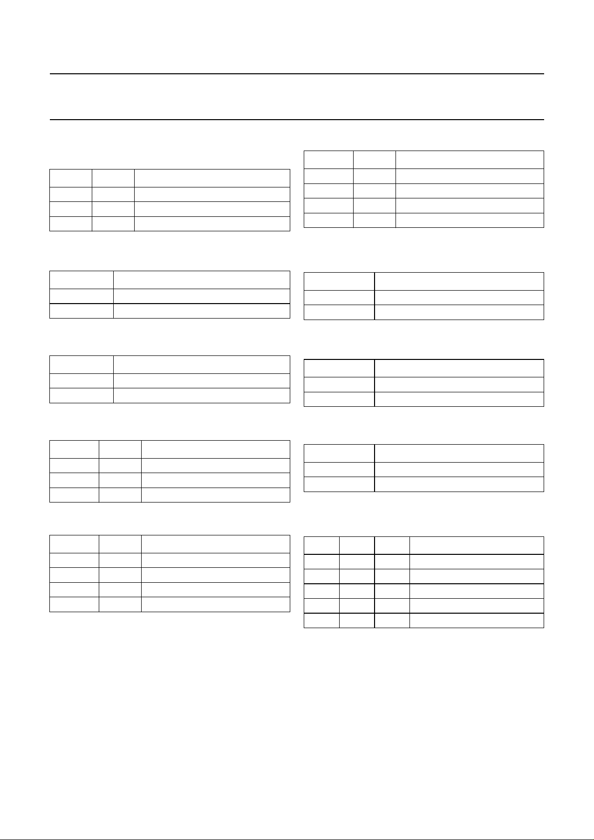
Table 4 Source select.
INA INB SOURCE
0 0 CVBS
01YC
1−auto CVBS/YC
Table 5 Trap bypass.
TB CONDITION
0 trap not bypassed
1 trap bypassed
Table 6 Comb filter enable.
ECMB CONDITION
0 comb filter disabled
1 comb filter enabled
Table 9 Forced field frequency.
FORF FORS FIELD FREQUENCY
0 0 auto; 60 Hz if no lock
0 1 60 Hz
1 0 50 Hz
1 1 auto; 50 Hz if no lock
Table 10 Output value I/O port.
OPA CONDITION
0 LOW
1 HIGH
Table 11 Output value O port.
OPB CONDITION
0 LOW
1 HIGH
Table 7 Phase 1 time constant.
FOA FOB MODE
0 0 auto
0 1 slow
1 − fast
Table 8 Crystal indication.
XA XB CRYSTAL
0 0 2 x 3.6 MHz
0 1 1 x 3.6 MHz
1 0 1 x 4.4 MHz
1 1 3.6 and 4.4 MHz
Table 12 Phase 1 loop control.
POC CONDITION
0 phase one loop closed
1 phase one loop open
Table 13 Forced standard.
FM SAF FRQF STANDARD
0 −−auto search
1 0 0 PAL/NTSC second crystal
1 0 1 PAL/NTSC reference crystal
1 1 0 illegal
1 1 1 SECAM reference crystal
Note to table 13
1. If XA and XB indicate that only one crystal is
connected to the IC and FM and FRQF force it to use
the second crystal the colour will be switched off.
December 1992 13
Page 14
Philips Semiconductors Product specification
PAL/NTSC/SECAM decoder/sync processor TDA9141
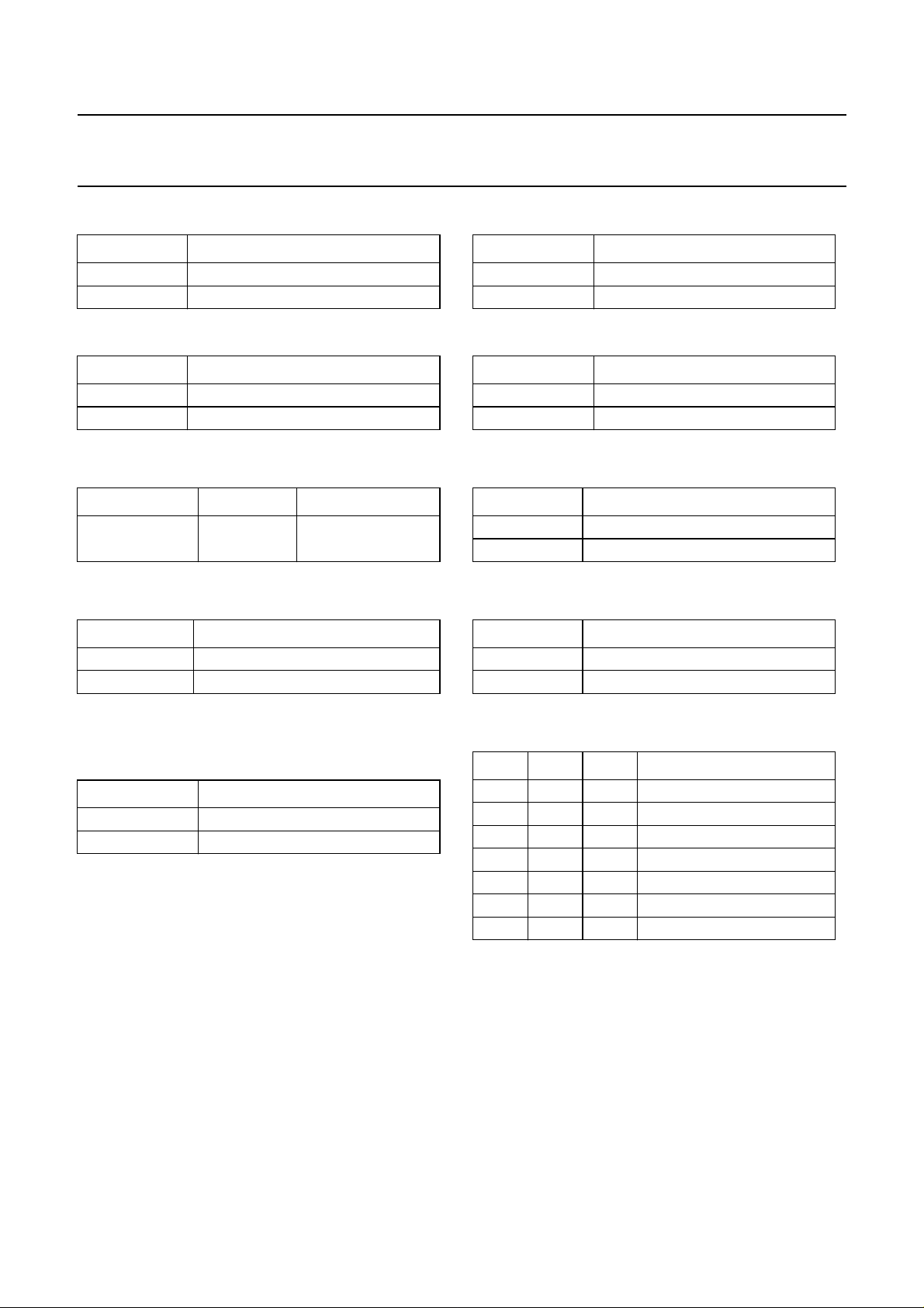
Table 14 Fast switch enable.
EFS CONDITION
0 fast switch disabled
1 fast switch enabled
Table 15 Search tuning mode.
STM CONDITION
0 search tuning mode off
1 search tuning mode on
Table 16 Hue.
FUNCTION ADDRESS DIGITAL NUMBER
hue HU5 to HU0 000000 = −45°
111111 = +45°
Table 17 Line-locked clock active.
LCA CONDITION
0 OPB/CLP mode
1 LLC/HA mode
Table 19 Field frequency indication.
FSI CONDITION
0 50 Hz
1 60 Hz
Table 20 Input switch mode.
YC CONDITION
0 CVBS mode
1 YC mode
Table 21 Phase 1 lock indication.
SL CONDITION
0 not locked
1 locked
Table 22 Input value I/O port.
IP CONDITION
0 LOW
1 HIGH
OUTPUT SIGNALS
Table 18 Power-on reset.
POR CONDITION
0 normal mode
1 power-down mode
Table 23 Standard read-out.
SAK SBK FRQ STANDARD
0 0 0 PAL second crystal
0 0 1 PAL reference crystal
0 1 0 NTSC second crystal
0 1 1 NTSC reference crystal
1 0 0 illegal forced mode
1 0 1 SECAM reference crystal
11−colour off
December 1992 14
Page 15
Philips Semiconductors Product specification
PAL/NTSC/SECAM decoder/sync processor TDA9141
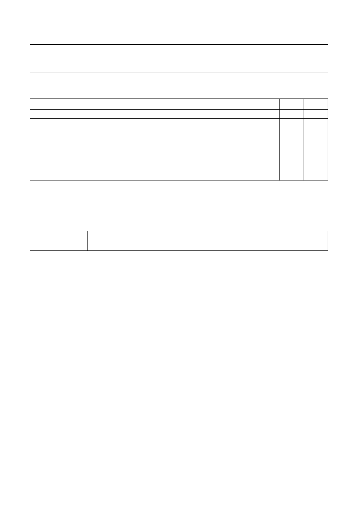
LIMITING VALUES
In accordance with the Absolute Maximum Rating System. (IEC134)
SYMBOL PARAMETER CONDITIONS MIN. MAX. UNIT
V
CC
I
CC
P
tot
T
stg
T
amb
ESD electrostatic discharge (on all pins)
Notes to the limiting values
1. Equivalent to discharging a 100 pF capacitor via a 1.5 kΩ series resistor.
2. Equivalent to discharging a 200 pF capacitor via a 0 Ω series resistor.
positive supply voltage − 8.8 V
supply current − 60 mA
total power dissipation − 530 mW
storage temperature −55 +150 °C
operating ambient temperature −10 +65 °C
Human body model note 1 −2000 +2000 V
Machine model note 2 −200 +200 V
THERMAL RESISTANCE
SYMBOL PARAMETER THERMAL RESISTANCE
R
th j-a
from junction to ambient in free air 48 K/W
December 1992 15
Page 16
Philips Semiconductors Product specification
PAL/NTSC/SECAM decoder/sync processor TDA9141
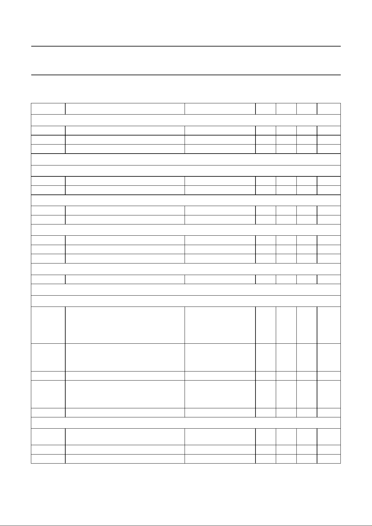
CHARACTERISTICS
= 8 V; T
V
CC
SYMBOL PARAMETER CONDITIONS MIN. TYP. MAX. UNIT
Supply
V
CC
I
CC
P
tot
Input switch
= 25 °C; unless otherwise specified.
amb
positive supply voltage 7.2 8.0 8.8 V
supply current − 45 − mA
total power dissipation − 360 − mW
Y/CVBS
V
26(p-p)
Z
I
INPUT (PIN 26)
input voltage (peak-to-peak value) top sync - white − 1.0 1.43 V
input impedance 60 −−kΩ
CINPUT (PIN 25)
V
25(p-p)
Z
I
input burst voltage (peak-to-peak value) − 0.3 0.43 V
input impedance 60 −−kΩ
CVBS OUTPUT (PIN 22) ONLY ADDRESS 8A
V
22(p-p)
Z
O
V
tsl
output voltage (peak-to-peak value) top sync - white − 1.0 − V
output impedance −−500 Ω
top sync voltage level − 2.8 − V
Bias generator (pin 8)
V
8
digital supply voltage − 5.0 − V
Subcarrier regeneration
ENERAL
G
CR catching range note 1
reference crystal 4.4 MHz ±400 −−Hz
reference crystal 3.6 MHz tbf −−Hz
second crystal 3.6 MHz ±300 −−Hz
ϕ phase shift
for 400 Hz deviation 4.4 MHz −−5 deg
for 300 Hz deviation 3.6 MHz −−5 deg
TC temperature coefficient of oscillator − tbf − Hz/K
Z
I
input impedance
reference crystal input − 1.0 − kΩ
second crystal input − 1.5 − kΩ
V
dep
supply voltage dependency − tbf − V
FSCOMB OUTPUT (PIN 23)
V
sub(p-p)
subcarrier output amplitude
CL = 15 pF 150 200 300 mV
(peak-to-peak value)
V
cen
V
cdis
comb enable voltage level 4.0 4.2 − V
comb disable voltage level − 0.8 1.4 V
December 1992 16
Page 17
Philips Semiconductors Product specification
PAL/NTSC/SECAM decoder/sync processor TDA9141
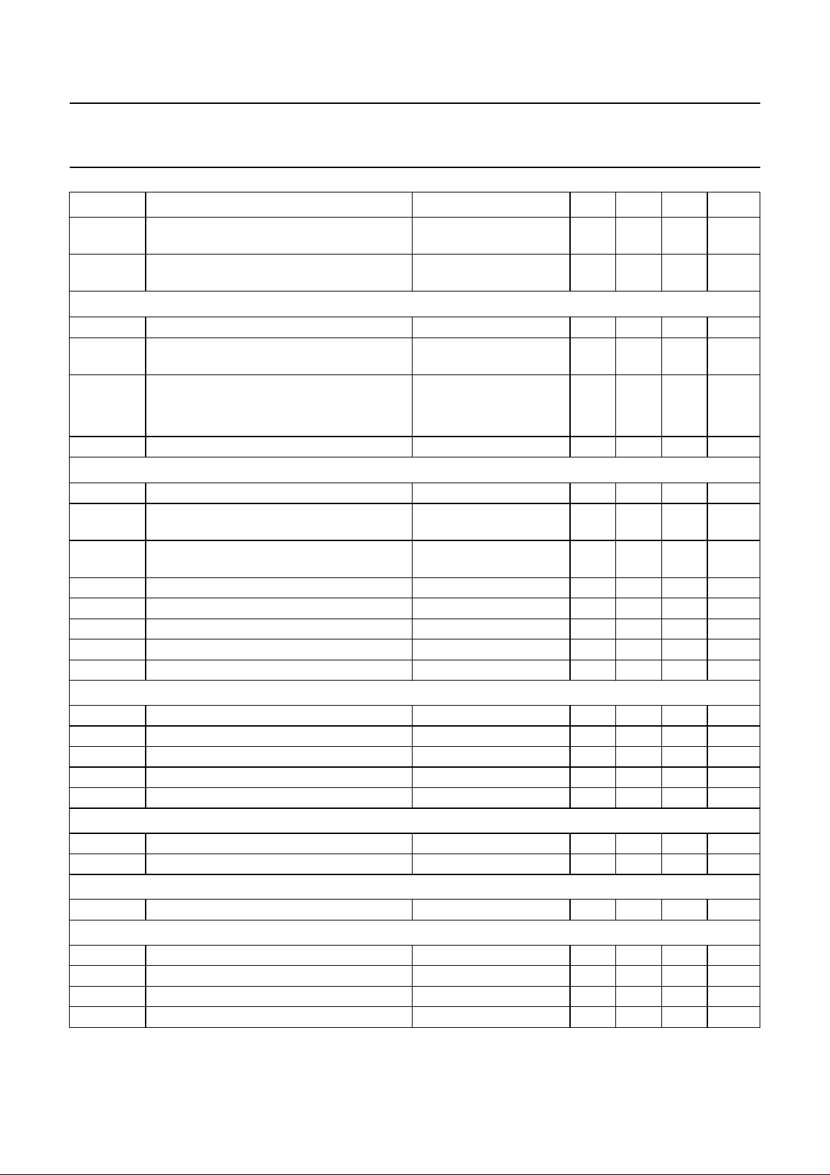
SYMBOL PARAMETER CONDITIONS MIN. TYP. MAX. UNIT
I
sink
R
GND
ACC
Demodulators −(R−Y) and −(B−Y) outputs (pins 1 and 2)
TC temperature coefficient of −(R−Y) and
V
1
V
2
B −3 dB bandwidth − 1 − MHz
Z
O
V
dep
PAL/NTSC DEMODULATOR
V
1(p-p)
V
2(p-p)
α crosstalk between −(R−Y) and −(B−Y) − tbf − dB
V
1,2(p-p)
V
1,2(p-p)
PAL DEMODULATOR
V
R(p-p)
S/N signal-to-noise ratio 46 −−dB
NTSC
ϕ hue phase shift −±45 − deg
SECAM DEMODULATOR
V
1(p-p)
V
2(p-p)
f
os
S/N signal-to-noise ratio − 43 − dB
minimum sink current to force output
0.4 − 2.0 mA
to comb disable level
value of grounded resistor to force output
0.4 − 2.0 kΩ
to comb disable level
ACC control range −20 − +5 dB
change of −(R−Y) and −(B−Y) signals over
−−1dB
ACC range
colour killer threshold
PAL/NTSC −−25 − dB
SECAM −−23 − dB
kill - unkill hysteresis − 3 − dB
ratio of −(R−Y) and −(B−Y) signals standard colour bar 1.20 1.27 1.34
− tbf − Hz/K
−(B−Y) amplitude
spread of −(R−Y) and −(B−Y) ratio between
−1 − +1 dB
standards
output level of −(R−Y) during blanking − 2.0 − V
output level of −(B−Y) during blanking − 2.0 − V
output impedance −−500 Ω
supply voltage dependency − tbf − V
−(R−Y) output voltage (peak-to-peak value) standard colour bar 470 525 585 mV
−(B−Y) output voltage (peak-to-peak value) standard colour bar 595 665 740 mV
8.8 MHz residue (peak-to-peak value) both outputs −−15 mV
7.2 MHz residue (peak-to-peak value) both outputs −−20 mV
H/2 ripple (peak-to-peak value) −−50 mV
DEMODULATOR
−(R−Y) output voltage (peak-to-peak value) standard colour bar 0.94 1.05 1.17 V
−(B−Y) output voltage (peak-to-peak value) standard colour bar 1.19 1.33 1.48 V
black level offset −−7 kHz
December 1992 17
Page 18
Philips Semiconductors Product specification
PAL/NTSC/SECAM decoder/sync processor TDA9141
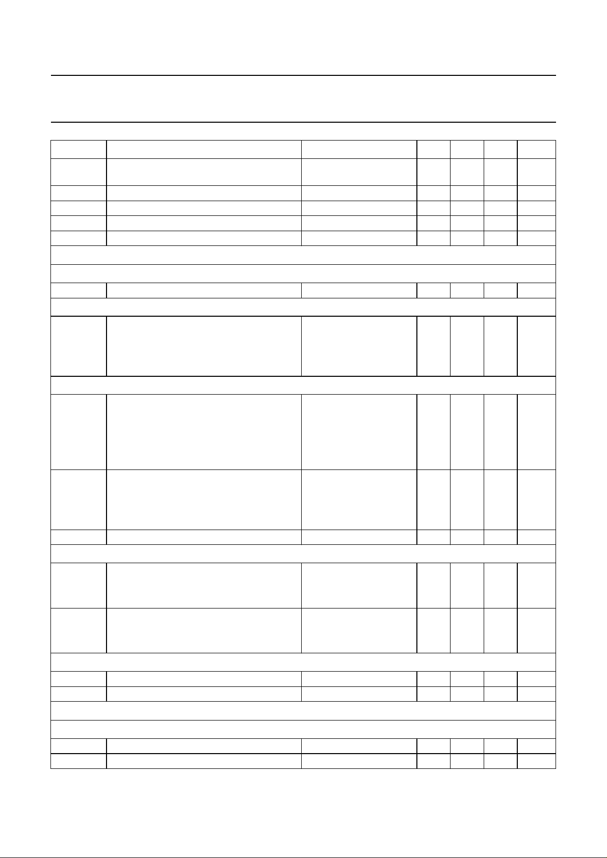
SYMBOL PARAMETER CONDITIONS MIN. TYP. MAX. UNIT
V
res(p-p)
f
pole
V
cal
NL non linearity −−3%
Filters
T
UNING
V
tune
LUMINANCE DELAY
t
d
C
HROMINANCE TRAP
f
O
B bandwidth at −3 dB
SUPP subcarrier suppression 26 −−dB
C
HROMINANCE BANDPASS
f
res
B bandwidth at −3 dB
CLOCHE FILTER
f
res
B bandwidth at −3 dB SECAM 241 268 295 kHz
7.8 to 9.4 MHz residue
−−30 mV
(peak-to-peak value)
pole frequency of de-emphasis 77 85 93 kHz
ratio of pole and zero frequency − 3 −
calibration voltage 345V
tuning voltage 1.5 3.0 6.0 V
delay time
PAL/NTSC − 480 − ns
SECAM − 480 − ns
B/W − 220 − ns
notch frequency
f
= 3.6 MHz 3.53 3.58 3.63 MHz
SC
f
= 4.4 MHz 4.37 4.43 4.49 MHz
SC
SECAM 4.23 4.29 4.35 MHz
YC mode; not active
f
= 3.6 MHz − 2.5 − MHz
SC
f
= 4.4 MHz − 3.1 − MHz
SC
SECAM − 3.0 − MHz
resonant frequency
= 3.6 MHz − 3.58 − MHz
f
SC
f
= 4.4 MHz − 4.43 − MHz
SC
fSC = 3.6 MHz − 1.4 − MHz
= 4.4 MHz − 1.7 − MHz
f
SC
resonant frequency SECAM 4.26 4.29 4.31 MHz
Sync input
VIDEO INPUT
V
26
sync pulse amplitude Y/CVBS input 50 300 600 mV
slicing level − 50 − %
December 1992 18
Page 19
Philips Semiconductors Product specification
PAL/NTSC/SECAM decoder/sync processor TDA9141
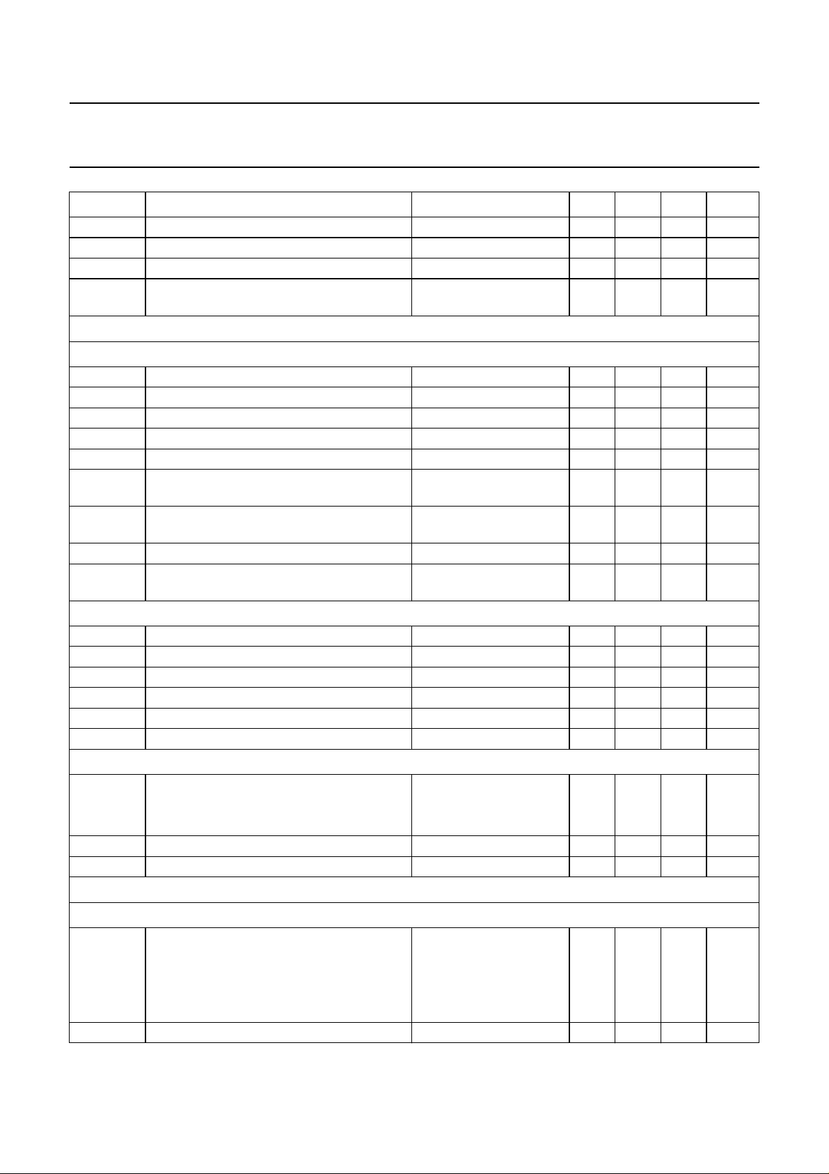
SYMBOL PARAMETER CONDITIONS MIN. TYP. MAX. UNIT
t
d
S/N noise detector threshold level − 20 − dB
H hysteresis − 3 − dB
t
d
Horizontal section
CLP
OUTPUT (OPB/CLP MODE); HAOUTPUT (LLC/HA MODE)
V
OH
V
OL
I
sink
I
source
t
W
t
d
t
d
t
W
t
d
FIRST LOOP
∆f frequency deviation when not locked −−1.5 %
SVRR supply voltage ripple rejection − tbf − V
TC temperature coefficient − tbf − Hz/°C
f
CR
f
HR
φ static phase shift −−0.1 µs/kHz
LLC
OUTPUT (LLC/HAMODE)
f
O
V
O(p-p)
V
O
Vertical section
delay of sync pulse due to internal filter 0.2 0.3 0.4 µs
delay between video signal and internally
12 18.5 27 µs
separated vertical sync pulse
HIGH level output voltage 4.0 5.0 5.5 V
LOW level output voltage I
= 2 mA − 0.2 0.4 V
sink
sink current 2 −−mA
source current 2 −−mA
HA pulse width (32 LLC pulses) − 4.7 −µs
delay between middle of horizontal sync
pulse and middle of H
A
delay between negative edge LLC pulse
note 2 0.3 0.45 0.6 µs
CL = 15 pF 10 20 40 ns
and positive edge HA pulse
CLP pulse width 21 LLC pulses − 3.1 −µs
delay between middle of horizontal sync
note 2 3.5 3.7 3.9 µs
pulse and start of CLP pulse
catching range ±625 −−Hz
holding range −−±1.4 kHz
output frequency
432f
432f
H
H
50 Hz standard − 6.75 − MHz
60 Hz standard − 6.80 − MHz
output amplitude (peak-to-peak value) CL = 15 pF 0.25 −−V
DC output voltage level − 2.5 − V
ERTICAL OSCILLATOR
V
f
fr
f
LR
free running frequency
frequency locking range 43 − 64 Hz
December 1992 19
FORF = 1;
divider ratio 628
FORF = 0;
divider ratio 528
− 50 − Hz
− 60 − Hz
Page 20
Philips Semiconductors Product specification
PAL/NTSC/SECAM decoder/sync processor TDA9141
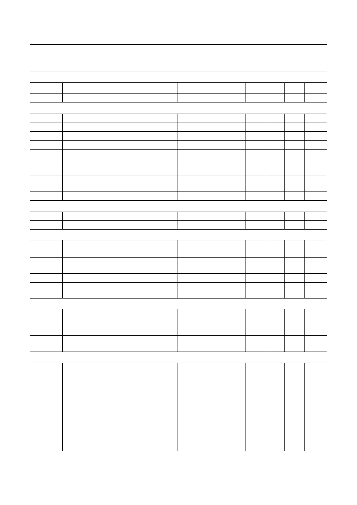
SYMBOL PARAMETER CONDITIONS MIN. TYP. MAX. UNIT
LR divider locking range 488 625 722
V
output
A
V
OH
V
OL
I
sink
I
source
t
W
t
d
Z
O
Sandcastle output (pin 10)
V
10
I
sink
HORIZONTAL AND VERTICAL BLANKING
V
bl
I
source
I
ext
t
W
t
d
CLAMPING PULSE
V
clamp
I
source
t
W
t
d
HIGH level output voltage 4.0 5.0 5.5 V
LOW level output voltage − 0.2 0.4 V
sink current 2 −−mA
source current 2 −−mA
VA pulse width
50 Hz standard − 160 −µs
60 Hz standard − 192 −µs
delay between start of vertical sync pulse
− 32 −µs
and positive edge of VA pulse
output impedance STM = 1 3 −−MΩ
zero level output voltage 0 0.5 1.0 V
sink current 0.5 −−mA
blanking voltage level 2.0 2.5 3.0 V
source current 0.5 −−mA
external current required to force the output
1.0 − 3.0 mA
to the blanking level
horizontal blanking pulse width 69 LLC pulses − 10.2 −µs
delay between start of horizontal blanking
45 LLC pulses − 6.7 −µs
and start of clamping pulse
clamping voltage level 4.0 4.5 5.0 V
source current 0.5 −−mA
pulse width 21 LLC pulses − 3.1 −µs
delay between middle sync of input and
note 2 3.5 3.7 3.9 µs
start of clamping pulse
Colour matrix
G
v
gain
from R to Y − 0.43 −
from G to Y − 0.84 −
from B to Y − 0.16 −
from R to U
from G to U
from B to U
from R to V
from G to V
from B to V
out
out
out
out
out
out
December 1992 20
− 0.43 −
− 0.84 −
− 1.27 −
− 1.00 −
− 0.84 −
− 0.16 −
Page 21
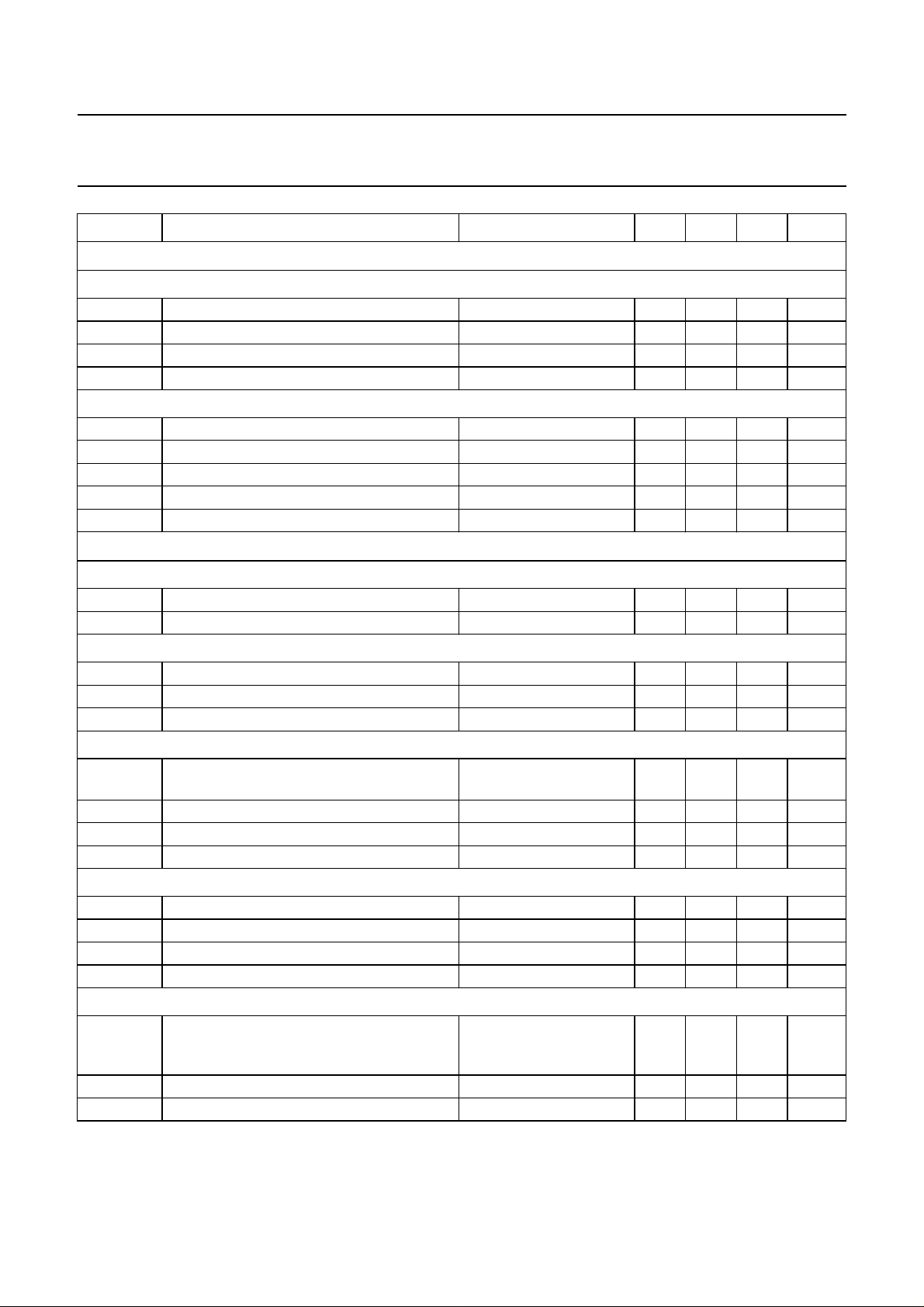
Philips Semiconductors Product specification
PAL/NTSC/SECAM decoder/sync processor TDA9141
SYMBOL PARAMETER CONDITIONS MIN. TYP. MAX. UNIT
Output and input/output port
O PORT (OPB/CLP MODE)
V
OH
V
OL
I
sink
I
source
I/O PORT (OPB/CLP MODE)
V
OH
V
OL
I
sink
V
IH
V
IL
YUV switches (note 3)
HIGH level output voltage 4.0 5.0 5.5 V
LOW level output voltage − 0.2 0.4 V
sink current 100 −−µA
source current 100 −−µA
HIGH level output voltage −−V
SUP
V
LOW level output voltage − 0.2 0.4 V
sink current 2 −−mA
HIGH level input voltage 2.0 −−V
LOW level input voltage −−0.6 V
RGB
INPUTS (NOTE 3)
V
Z
I(p-p)
I
input voltage (peak-to-peak value) note 4 − 0.7 1.0 V
input impedance 3 −−MΩ
UV INPUTS (NOTE 3)
V
V
Z
I(p-p)
I(p-p)
I
U input voltage (peak-to-peak value) note 3 − 1.33 1.90 V
V input voltage (peak-to-peak value) − 1.05 1.50 V
input impedance (both inputs) 3 −−MΩ
YOUTPUT
V
O(p-p)
U output voltage (peak-to-peak value) note 4;
− 1.43 − V
top sync-to-white
Z
O
V
O
output impedance −−250 Ω
DC output voltage level top sync − 2.5 − V
S/N signal-to-noise ratio − tbf − dB
UV
OUTPUTS (NOTE 3)
V
O(p-p)
V
O(p-p)
Z
O
V
O
U output voltage (peak-to-peak value) − 1.33 1.90 V
V output voltage (peak-to-peak value) − 1.05 1.50 V
output impedance (both outputs) −−250 Ω
DC output voltage level − 2.7 − V
GENERAL
V
diff
difference between black levels of
sync locked −−10 mV
YUV outputs in RGB mode
and YUV mode
NL non-linearity any input to any output −−5%
B bandwidth any input to any output − 7 − MHz
December 1992 21
Page 22
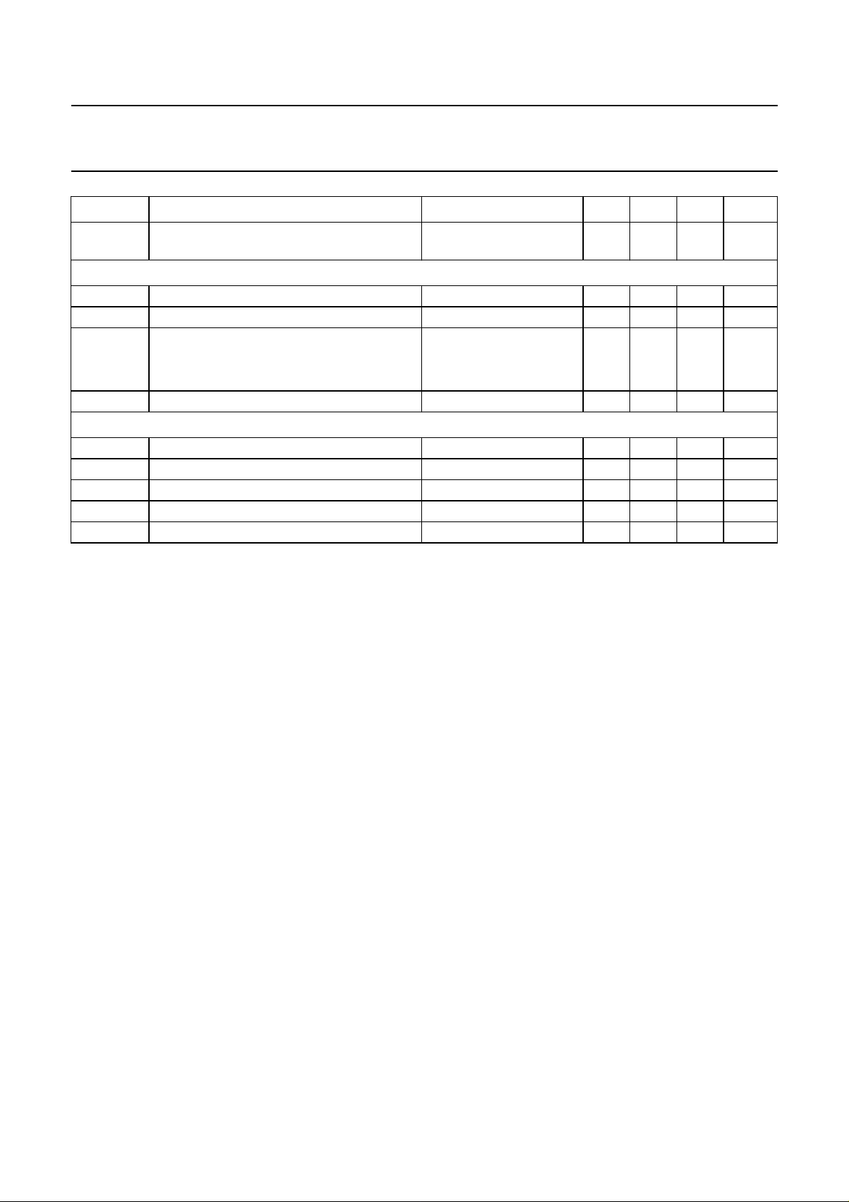
Philips Semiconductors Product specification
PAL/NTSC/SECAM decoder/sync processor TDA9141
SYMBOL PARAMETER CONDITIONS MIN. TYP. MAX. UNIT
CT crosstalk between RGB and UV
UV
out
FAST SWITCH SELECT INPUT (PIN 18)
V
IH
V
IL
G
v
t
d
HIGH level input voltage RGB switched on 0.9 − 3.0 V
LOW level input voltage UV switched on 0 − 0.5 V
gain
in
in
to U
to V
out
out
from U
from V
switching delay between pin 18 and YUV −−20 ns
INPUT CLAMP (PIN 17)
V
IH
V
IL
t
W
V
os
Z
I
HIGH level input voltage clamping 2.4 − 5.5 V
LOW level input voltage no clamping 0 − 0.6 V
clamping pulse width 1.8 3.5 −µs
clamping offset voltage on UV outputs −−10 mV
input impedance STM = 1 3 −−MΩ
Notes to the characteristics
1. All oscillator specifications are measured with the Philips crystal series 4322 143/144. If the spurious response of the
reference crystal is less than −3 dB with respect to the fundamental frequency for a damping resistance of 1 kΩ,
oscillation at the fundamental frequency is guaranteed. The spurious response of the second crystal must be less
than −3 dB with respect to the fundamental frequency for a damping resistance of 1.5 kΩ.
The catching and detuning range are measured for nominal crystal parameters. These are:
load resonance frequency f0 (CL = 20 pF) = 4.433619 MHz, (second crystal: 3.579545 MHz)
motional capacitance CM = 20.6 fF, (second crystal: 14.7 fF)
parallel capacitance C0 = 5.5 pF, (second crystal: 4.5 pF).
The actual load capacitance in the application should be CL = 18 pF to account for parasitic capacitances on and off
chip.
2. This delay is caused by the low pass filter at the sync separator input.
3. The output signals of the demodulator are called −(R−Y) and −(B−Y). The colour difference input and output signals
of the YUV switch are called UV signals. However, these signals do not have the amplitude correction factor of real
UV signals. They are called UV signals and not −(R−Y) and −(B−Y) to prevent confusion between the colour
difference signals of the demodulator and the colour difference signals of the YUV switch.
4. This value refers to signals including a sync pulse. For Y signals composed to the RGB inputs this output voltage is
30% lower, as there is no sync pulse on such signals.
signals on
in
f = 0 to 5 MHz −−−50 dB
− 1 −
− 1 −
December 1992 22
Page 23
Philips Semiconductors Product specification
PAL/NTSC/SECAM decoder/sync processor TDA9141
QUALITY SPECIFICATION
Quality level in accordance with URV 4-2-59/601.
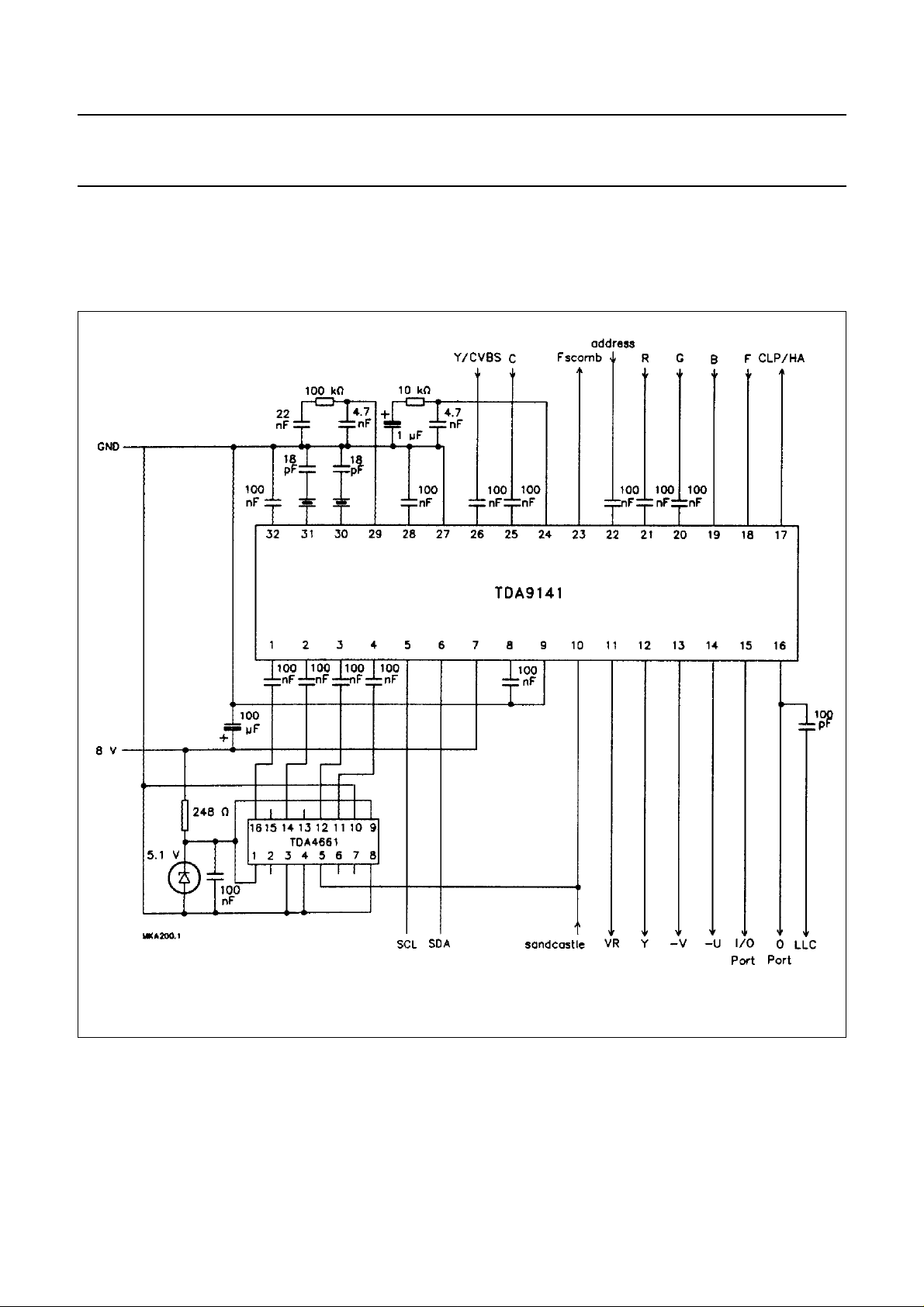
TEST AND APPLICATION INFORMATION
Fig.8 Application diagram.
Notes to figure 8
1. Pins 28 and 32 are sensitive to leakage current.
2. The analog and digital ground currents should be completely separated.
3. The decoupling capacitor connected between pins 8 and 9 must be placed as close to the IC as possible.
December 1992 23
Page 24
Philips Semiconductors Product specification
PAL/NTSC/SECAM decoder/sync processor TDA9141
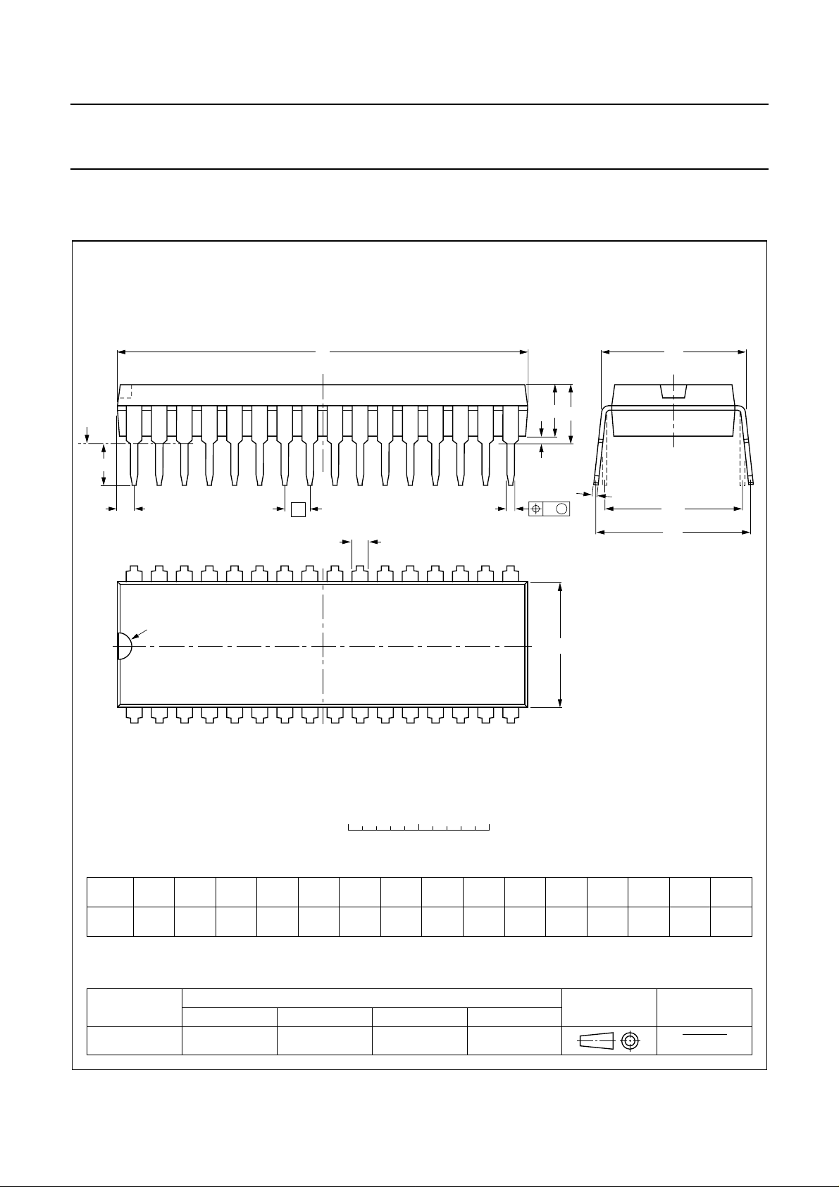
PACKAGE OUTLINE
SDIP32: plastic shrink dual in-line package; 32 leads (400 mil)
D
seating plane
L
Z
32
pin 1 index
e
b
SOT232-1
M
E
A
2
A
A
1
w M
b
1
17
E
c
(e )
M
1
H
1
0 5 10 mm
scale
DIMENSIONS (mm are the original dimensions)
A
A
A
UNIT b
Note
1. Plastic or metal protrusions of 0.25 mm maximum per side are not included.
mm
OUTLINE
VERSION
SOT232-1
max.
4.7 0.51 3.8
12
min.
max.
IEC JEDEC EIAJ
1.3
0.8
b
1
0.53
0.40
REFERENCES
0.32
0.23
cEe M
(1) (1)
D
29.4
28.5
December 1992 24
9.1
8.7
16
(1)
Z
L
3.2
2.8
EUROPEAN
PROJECTION
M
10.7
10.2
E
12.2
10.5
e
1
w
H
0.181.778 10.16
ISSUE DATE
92-11-17
95-02-04
max.
1.6
Page 25
Philips Semiconductors Product specification
PAL/NTSC/SECAM decoder/sync
processor
SOLDERING
Introduction
There is no soldering method that is ideal for all IC
packages. Wave soldering is often preferred when
through-hole and surface mounted components are mixed
on one printed-circuit board. However, wave soldering is
not always suitable for surface mounted ICs, or for
printed-circuits with high population densities. In these
situations reflow soldering is often used.
This text gives a very brief insight to a complex technology.
A more in-depth account of soldering ICs can be found in
“IC Package Databook”
our
Soldering by dipping or by wave
The maximum permissible temperature of the solder is
260 °C; solder at this temperature must not be in contact
DEFINITIONS
(order code 9398 652 90011).
TDA9141
with the joint for more than 5 seconds. The total contact
time of successive solder waves must not exceed
5 seconds.
The device may be mounted up to the seating plane, but
the temperature of the plastic body must not exceed the
specified maximum storage temperature (T
printed-circuit board has been pre-heated, forced cooling
may be necessary immediately after soldering to keep the
temperature within the permissible limit.
Repairing soldered joints
Apply a low voltage soldering iron (less than 24 V) to the
lead(s) of the package, below the seating plane or not
more than 2 mm above it. If the temperature of the
soldering iron bit is less than 300 °C it may remain in
contact for up to 10 seconds. If the bit temperature is
between 300 and 400 °C, contact may be up to 5 seconds.
stg max
). If the
Data sheet status
Objective specification This data sheet contains target or goal specifications for product development.
Preliminary specification This data sheet contains preliminary data; supplementary data may be published later.
Product specification This data sheet contains final product specifications.
Limiting values
Limiting values given are in accordance with the Absolute Maximum Rating System (IEC 134). Stress above one or
more of the limiting values may cause permanent damage to the device. These are stress ratings only and operation
of the device at these or at any other conditions above those given in the Characteristics sections of the specification
is not implied. Exposure to limiting values for extended periods may affect device reliability.
Application information
Where application information is given, it is advisory and does not form part of the specification.
LIFE SUPPORT APPLICATIONS
These products are not designed for use in life support appliances, devices, or systems where malfunction of these
products can reasonably be expected to result in personal injury. Philips customers using or selling these products for
use in such applications do so at their own risk and agree to fully indemnify Philips for any damages resulting from such
improper use or sale.
2
PURCHASE OF PHILIPS I
C COMPONENTS
Purchase of Philips I
components in the I2C system provided the system conforms to the I2C specification defined by
Philips. This specification can be ordered using the code 9398 393 40011.
December 1992 25
2
C components conveys a license under the Philips’ I2C patent to use the
 Loading...