

Page 1

INTEGRATED CIRCUITS
DATA SH EET
TDA8822
Universal I
2
C-bus programmable
RF modulator
Preliminary specification
File under Integrated Circuits, IC02
1997 Jan 08
Page 2

Philips Semiconductors Preliminary specification
Universal I2C-bus programmable RF
modulator
FEATURES
• 5 V power supply
• Video amplifier with clamp and white clip circuits
• Programmable video modulation depth
• FM sound modulator (4.5, 5.5, 6.0 and 6.5 MHz)
• Programmable picture-to-sound ratio
• Programmable deviation of the sound subcarrier
• Input for modulated NICAM sound subcarrier or second
frequency modulated sound subcarrier
• Asymmetrical or symmetrical RF output buffer
• Symmetrical RF oscillator for UHF or VHF band
according to the application
• One I2C-bus programmable output port
• On-chip Phase-Locked Loop (PLL) frequency
synthesizer for the RF carrier
• On-chip PLL frequency synthesizer for the sound carrier
• On-chip power supply regulator
• On-chip I2C-bus and/or hardware controlled Test
Pattern Signal Generator (TPSG) with LED driver
• RF output switch-off during tuning.
APPLICATIONS
• Video recorders
• Cable converters
• Satellite receivers
• Set top boxes.
TDA8822
GENERAL DESCRIPTION
The TDA8822 is a programmable modulator which
generates an RF TV channel from a baseband video
signal and a baseband audio signal in the event of
negative video and FM sound standards (B/G, I, D/K, M
and N standards).
Two PLL frequency-synthesizers set the picture carrier
frequency and the sound subcarrier frequency to the
required frequencies. These PLL frequency-synthesizers
are programmed via the I
The I2C-bus controls these features:
• Video modulation depth
• Sound subcarrier modulation deviation
• Picture-to-sound ratio.
This makes the IC suitable for multistandard applications
without any adjustment into the application.
Additional features are provided like an input for the
NICAM or second FM carrier, a test pattern signal
generator with a LED driver and a general purpose
output port.
2
C-bus.
ORDERING INFORMATION
TYPE
NUMBER
TDA8822T SO24 plastic small outline package; 24 leads; body width 7.5 mm SOT137-1
TDA8822M SSOP24 plastic shrink small outline package; 24 leads; body width 5.3 mm SOT340-1
1997 Jan 08 2
NAME DESCRIPTION VERSION
PACKAGE
Page 3

Philips Semiconductors Preliminary specification
Universal I2C-bus programmable RF
TDA8822
modulator
QUICK REFERENCE DATA
V
CCA=VCCD
PS setting = 1; video input signal = 500 mV (p-p) EBU colour bars; audio input signal = 45 mV (p-p); 1 kHz sine wave;
unless otherwise specified.
SYMBOL PARAMETER CONDITIONS MIN. TYP. MAX. UNIT
V
CCA
V
CCD
I
CC(tot)
m
d
P/S picture-to-sound ratio
V
RF
f
sc
∆f
sc
=5V; T
=25°C; in PAL B/G, PAL I, PAL D/K or NTSC; MD setting = 4; DEV setting = 2;
amb
analog supply voltage 4.5 5.0 5.5 V
digital supply voltage 4.5 5.0 5.5 V
total supply current − 60 72 mA
modulation depth adjustment
range
adjustment range
RF output voltage level
typical value for MD setting between
72.5 − 90.0 %
0 and 7
typical value for PS setting between
−18 −−11 dB
0 and 7
frequency between 45 and 860 MHz 77 80 83 dBµV
asymmetrical on a 75 Ω load
sound subcarrier frequency 4.5 − 6.5 MHz
sound subcarrier frequency
deviation range
for B/G, I, D/K, SC setting = 1, 2 or 3;
typical value for DEV setting between
20 − 45 kHz
0 and 7
for M, N, SC setting = 0; typical value
10 − 22.5 kHz
for DEV setting between 0 and 7
1997 Jan 08 3
Page 4
Philips Semiconductors Preliminary specification
Universal I2C-bus programmable RF
modulator
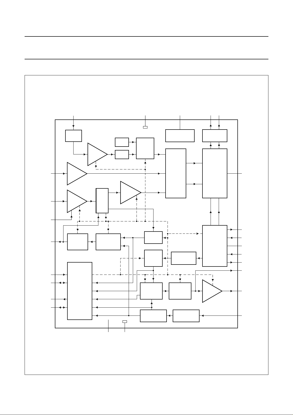
BLOCK DIAGRAM
handbook, full pagewidth
NICAM
VIDEO
24
CLAMP
TPSG
VIDEO
AMP.
MD setting
21
NICAM
AMP.
CLIP
AGND
23
SWITCH
TPSG
ON/OFF
V
CCA
1
VOLTAGE
REGULATOR
ADDER
RFA RFB
OUTPUT
BUFFER
MIXER
1819
TDA8822
20
RFGND
AUDIO
PREEMPH
ACP
SCL
SDA
P0
TPSG
SND-IF
22
AUDIO
AMP.
DEV
setting
3
test test
2
14
15
16
17
AUDIO
CHARGE
PUMP
2
I
C-BUS
RECEIVER
AND
LOGIC
VCO
AUDIO
PHASE
DETECTOR
I2C-bus control
f
div(audio)
f
div(video)
in-lock flag
f
ref(video)
f
ref(audio)
V
CCD
AMP.
setting
sound oscillator
ON/OFF
frequency
setting
11 13
DGND
PS
PROG.
DIVIDER
14 BITS
PROG.
DIVIDER
test test
VIDEO
PHASE
DETECTOR
REFERENCE
DIVIDER
frequency
setting
PRESCALER
DIVIDE-BY-8
CHARGE
TDA8822
RF oscillator
ON/OFF
VIDEO
PUMP
CRYSTAL
OSCILLATOR
RF
OSCILLATOR
test
LOOP
AMP.
10
12
MGE674
4
5
6
7
8
9
RFOSCA
RFOSCB
OGND
RFOSCC
RFOSCD
VCP
VVT
XTAL
Fig.1 Block diagram.
1997 Jan 08 4
Page 5
Philips Semiconductors Preliminary specification
Universal I2C-bus programmable RF
modulator
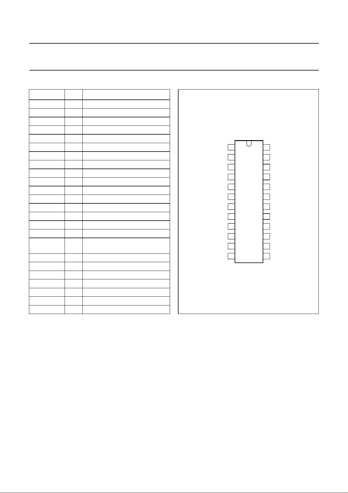
PINNING
SYMBOL PIN DESCRIPTION
V
CCA
ACP 2 audio charge pump output
PREEMPH 3 audio pre-emphasis network
RFOSCA 4 RF oscillator A (collector) output
RFOSCB 5 RF oscillator B (base) input
OGND 6 RF oscillator ground
RFOSCC 7 RF oscillator C (base) input
RFOSCD 8 RF oscillator D (collector) output
VVT 9 video tuning voltage output
VCP 10 video charge pump output
V
CCD
XTAL 12 crystal oscillator input
DGND 13 digital ground
SCL 14 serial clock (I
SDA 15 serial data (I
P0 16 general purpose output
TPSG 17 test pattern signal generator
RFB 18 RF output B
RFA 19 RF output A
RFGND 20 ground for the RF outputs
NICAM 21 NICAM input
AUDIO 22 audio input
AGND 23 analog ground
VIDEO 24 video input
1 analog power supply
11 digital power supply
2
C-bus) input
2
C-bus) input/output
input/output pin
handbook, halfpage
PREEMPH
RFOSCA
RFOSCB
RFOSCC
RFOSCD
V
1
CCA
ACP
2
3
4
5
OGND
6
TDA8822
7
8
VVT
9
VCP
10
V
11
CCD
XTAL
12
MGE673
Fig.2 Pin configuration.
TDA8822
VIDEO
24
AGND
23
AUDIO
22
NICAM
21
RFGND
20
19
RFA
RFB
18
17
TPSG
P0
16
SDA
15
SCL
14
DGND
13
1997 Jan 08 5
Page 6
Philips Semiconductors Preliminary specification
Universal I2C-bus programmable RF
modulator
FUNCTIONAL DESCRIPTION
The TDA8822 is a programmable RF modulator which can
be divided into the following parts:
• Video part
• Audio part
• RF part.
Video part
The video part provides the following:
• The video part includes a clamping circuit which sets the
internal reference voltage to the bottom of the
synchronizing pulse. The modulation depth is adjusted
using 3 bits of the I
MD1 and MD0. These 3 bits make 8 different values for
the modulation depth possible (see Table 1).
• After the modulation depth is set, the signal is fed
through a clip control circuit that clips the video signal to
avoid that the modulation depth becomes higher than
100%.
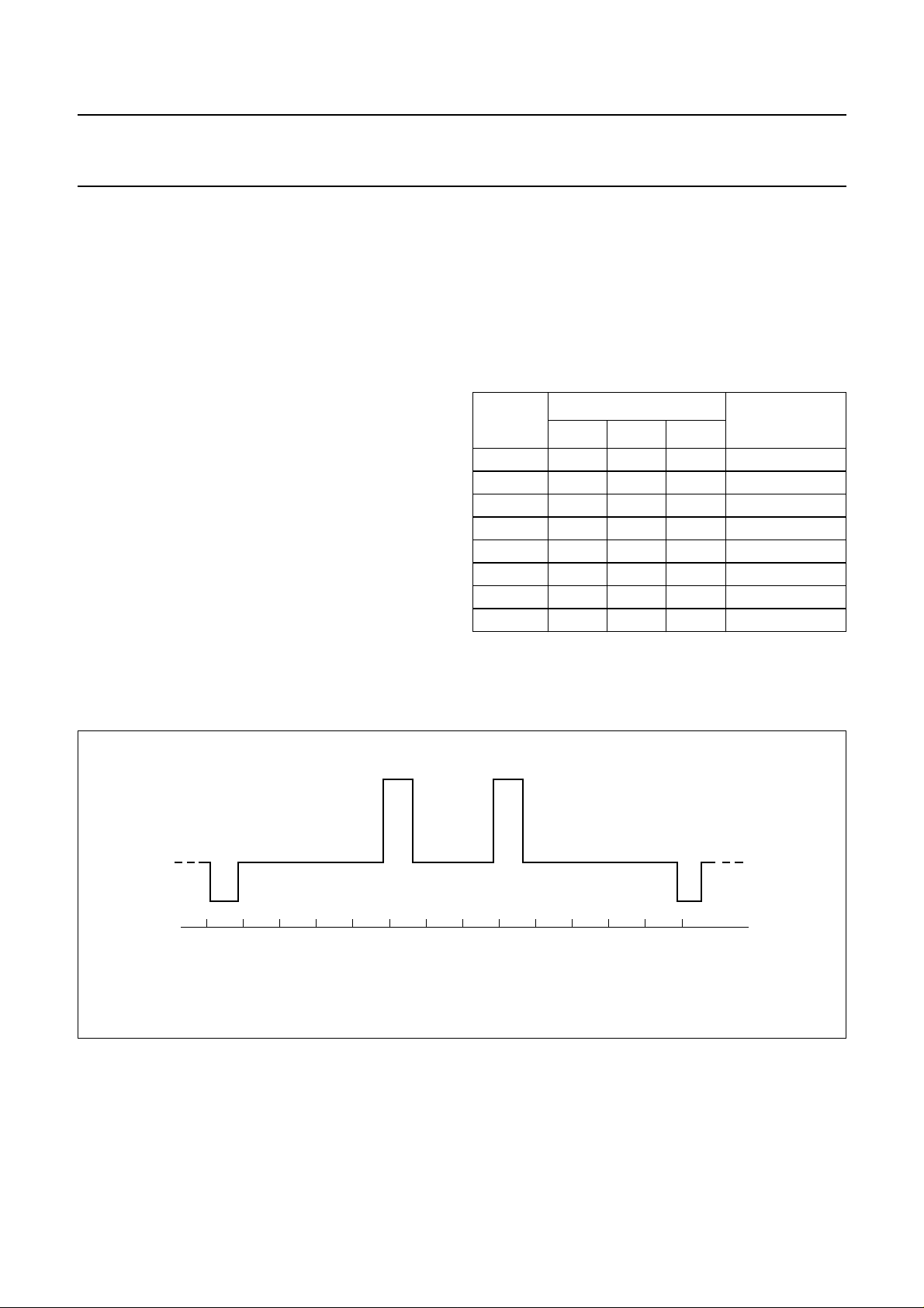
• The video part also contains a TPSG. This TPSG
generates a pattern that helps to tune the TV set to the
programmed channel of the modulator. The pattern
consists of a sync pulse and two vertical white bars on
the screen (see Fig.3)
2
C-bus programming, called MD2,
TDA8822
The TPSG is activated in two ways:
– Forcing the pin TPSG to DGND in the application
(see Fig.8)
– Setting the TPSG bit to 1 via the I2C-bus, then the
TPSG pin acts as an output port, sinking current to
allow the indication of the use of the TPSG in the
application e.g. with an LED (see Fig.9).
Table 1 Modulation depth setting (typical values)
MD
SETTING
0 0 0 0 72.5
1 0 0 1 75.0
2 0 1 0 77.5
3 0 1 1 80.0
4 1 0 0 82.5
5 1 0 1 85.0
6 1 1 0 87.5
7 1 1 1 90.0
MD2 MD1 MD0
BIT
MODULATION
DEPTH (%)
handbook, full pagewidth
0 5 10 15 20 25 30 35 40 45 50 55 60 65 t (µs)
Fig.3 Test pattern signal.
1997 Jan 08 6
MGE675
Page 7

Philips Semiconductors Preliminary specification
Universal I2C-bus programmable RF
modulator
Audio part
The audio part provides the following:
• The sound subcarrier is created in an integrated VCO.
The signal at the output of this VCO is fed to a stage that
adjusts the picture-to-sound ratio and to the audio
programmable divider.
• The frequency of the sound subcarrier is set by
programming the bits SC1 and SC0 of the I2C-bus (see
Table 2). These two bits set the dividing ratio of the
audio programmable divider to get the divided frequency
f
div(audio)
• The audio phase detector compares the
phase/frequency of the divided audio frequency f
and the reference frequency for the audio, f
drives the Charge Pump (CP) that charges or
discharges the audio loop filter connected between
pins ACP and AGND to get the VCO oscillating to the
programmed frequency.
.
div(audio)
ref(audio)
and
TDA8822
• f
ref(audio)
purpose output port during a special test mode.
• The frequency deviation of the sound subcarrier is set
using 3 bits DEV2, DEV1 and DEV0 of the I2C-bus
programming (see Table 3), when a signal of 1 kHz with
a level of 50 mV (p-p) is applied on the audio input pin.
• The difference between the picture carrier level and the
sound subcarrier level is adjusted using 3 bits PS2, PS1
and PS0 (see Table 4).
• The NICAM amplifier has a constant gain, and is
designed for adding a second sound subcarrier in the TV
channel. This subcarrier can be either a second FM
carrier for dual-sound/stereo system used in PAL B/G or
a modulated NICAM carrier. The level between the
picture carrier and the NICAM carrier (P/N) will depend
on the input level on the NICAM input.
and f
div(audio)
can be monitored on the general
Table 2 Sound subcarrier frequency setting
SC SETTING
BIT
SC1 SC0
0 0 0 4.5 M, N
1 0 1 5.5 B, G
2 1 0 6.0 I
3 1 1 6.5 D, K
Table 3 Sound subcarrier frequency deviation setting (typical values)
BIT
DEV SETTING
DEV2 DEV1 DEV0 B, G, I, D, K M, N
0 0 0 0 40.0 20.0 10.0
1 0 0 1 45.0 22.5 11.3
2 0 1 0 50.5 25.3 12.6
3 0 1 1 56.5 28.3 14.1
4 1 0 0 63.5 31.8 15.9
5 1 0 1 71.5 35.8 17.9
6 1 1 0 80.0 40.0 20.0
7 1 1 1 90.0 45.0 22.5
SOUND SUBCARRIER
FREQUENCY (MHz)
DEVIATION
(%)
STANDARD
DEVIATION (kHz)
1997 Jan 08 7
Page 8

Philips Semiconductors Preliminary specification
Universal I2C-bus programmable RF
modulator
Table 4 Picture-to-sound ratio setting (typical values)
PS SETTING
PS2 PS1 PS0
0 000 −11
1 001 −12
2 010 −13
3 011 −14
4 100 −15
5 101 −16
6 110 −17
7 111 −18
RF part
The RF part provides the following:
• The RF oscillator can produce any frequency used for
TV transmission, from 35 to 890 MHz. The frequency
range depends on the components used in the
application (see Table 11).
• The RF mixer combines the video signal, the sound
subcarrier and the carrier from the NICAM input to build
a baseband TV channel. This baseband signal is then
mixed with the RF oscillator signal to get the RF TV
channel.
• The two signals from the RF mixer are sent to the output
buffer. This output buffer can be used either as two
asymmetrical outputs or as one symmetrical output.
• The output buffer is switched-off while the PLL is not
in-lock, to avoid parasitic output signal during the tuning
of the RF oscillator. The in-lock information is given by
the phase detector of the loop.
• The signal from the RF oscillator is fed to the PLL which
controls the picture carrier frequency. The RF signal is
first divided by 8 in the prescaler, and then divided in the
programmable 14-bits divider. The dividing ratio of this
divider is programmed via the I2C-bus. The minimum
frequency that can be synthesized is 16 MHz, and the
maximum frequency is 1023.9375 MHz.
• The divided frequency called f
reference frequency called f
div(video)
ref(video)
is compared to the
coming from the
crystal oscillator and divided in the reference divider.
The crystal oscillator is intended to be used with a
crystal of 4 MHz.
• The comparison between f
ref(video)
and f
div(video)
in the video phase detector. The resulting signal is fed
via the video charge pump to the loop amplifier,
including the tuning voltage drive (33 V) inside the IC.
BIT
is done
TDA8822
P/S RATIO
(dB)
• f
ref(video)
and f
div(video)
output port during a special test mode.
• The I2C-bus receiver and control logic includes the
control of:
– Picture carrier frequency
– Sound subcarrier frequency
– Sound subcarrier frequency deviation
– Video modulation depth
– Picture-to-sound ratio
– TPSG on/off and LED drive control
– RF oscillator on/off
– Sound oscillator on/off
– General purpose output port on/off
– Test modes setting.
Software information
The transmission is made using 4 words in I
First the address CA has to be sent, then at least two
consecutive words have to be sent, either the two words
F1 and F0, or the two words C1 and C0.
The two words C1 and F1 are differentiated inside the IC
by the first bit being logic 1 or logic 0 respectively.
The contents of the 4 bytes is shown in Table 5.
At the power-up of the TDA8822, the I2C-bus state is the
following:
• N13 to N0 are not fixed
• SC setting = 1: the sound carrier is fixed to 5.5 MHz
• MD is set to 4 (82.5%), PS is set to 1 (−12 dB) and DEV
is set to 2 (50.5%)
can also be monitored on the
2
C-bus format.
1997 Jan 08 8
Page 9

Philips Semiconductors Preliminary specification
Universal I2C-bus programmable RF
modulator
• T0 is set to logic 1, RF0 is set to logic 1, TPSG is set to
logic 1 and P0 is set to logic 0 to select the video high
impedance test mode because it is in this mode that the
RF oscillator starts in the best conditions.
The TPSG bit is used to switch on or off the TPSG using
the I2C-bus. It is also possible to switch the TPSG on in the
application, connecting the pin TPSG to DGND. This
pin TPSG has a double function and acts as an input or as
an output.
These are the two functions:
• Output: if the TPSG is set using the I2C-bus, the
pin TPSG is used as an output open collector NPN port.
This port can be used to indicate with an LED that the
TPSG is on. This is especially useful in systems using
an on-screen display. If the TV set is not tuned to the
right channel there is an alternate indication that the
TPSG is on (see Fig.9).
• Input: if the TPSG is set with an hardware switch in the
application, the TPSG pin is used as one of the inputs to
select the TPSG mode (see Fig.8).
Notice that if the TPSG bit is set to logic 1 while the RF0
bit is set to logic 0, the TPSG is turned off, and the sound
oscillator is off (see Table 8).
N13 to N0 are the 14 bits to set the video programmable
divider ratio and then to set the picture carrier frequency
following the formula: f
where:
• f
ref(video)
reference divider ratio. For example, with a 4 MHz
crystal connected to
pin XTAL,f
is the frequency on pin XTAL divided by the
ref video()
osc=fref(video)
4000000
----------------------- 512
× 8 × N,
7812.5 Hz==
TDA8822
• N is the programmable divider ratio:
N=N
• f
osc
DEV2, DEV1 and DEV0 are the bits to set the sound
subcarrier frequency deviation (see Table 3).
PS2, PS1 and PS0 are the bits to set the picture-to-sound
ratio (see Table 4).
MD2, MD1 and MD0 are the bits to set the modulation
depth (see Table 1).
SC1 and SC0 are the bits to set the sound subcarrier
frequency according to Table 2.
RF0 is a bit that controls the RF oscillator on/off. In normal
mode, it should be set to logic 1. If the modulator is not
used and may create some interferences with other
signals in the application, it should be set to logic 0
(see Table 6).
Notice that if the bit RF0 is logic 0 while the bit TPSG is
logic 1, then the RF oscillator is still running, but the sound
oscillator is off, and the TPSG is also off (see Table 8).
The bit P0 controls the output port P0, which is an open
collector NPN port, able to drive up to 10 mA
(see Table 7).
T0 is a bit used for test purposes. If this bit is set to logic 0,
the IC operates in normal configuration. If it is set to
logic 1, then the use of bits TPSG, RF0 and P0 is changed
to select 1 of the 8 test modes as explained in Table 9.
× 213+N12× 212+ ... + N1× 2+N
13
is the RF oscillator frequency.
0
Table 5 Contents of programming words
BYTE
Address byte CA 11001010 ACK
F1: frequency
byte 1
F0: frequency
byte 0
C1: control byte 1 1 DEV2 DEV1 DEV0 PS2 PS1 PS0 0 ACK
C0: control byte 0 MD2 MD1 MD0 SC1 SC0 RF0 P0 T0 ACK
1997 Jan 08 9
MSB LSB
ACKNOWLEDGE BIT
BIT 7 BIT 6 BIT 5 BIT 4 BIT 3 BIT 2 BIT 1 BIT 0
0 TPSG N13 N12 N11 N10 N9 N8 ACK
N7 N6 N5 N4 N3 N2 N1 N0 ACK
Page 10

Philips Semiconductors Preliminary specification
Universal I2C-bus programmable RF
modulator
Table 6 RF oscillator on/off setting (see note 1)
STATE OF RF0 ACTION ON RF OSCILLATOR
0 stopped; no RF carrier
1 operating; normal use
Note
1. This table is valid only if bit TPSG is set to logic 0.
Table 7 Output port programming
STATE OF P0 PORT STATE
0 high impedance close to V
1 sinking current close to 0 V
Table 8 Overview of the normal modes
T0 RF0 TPSG P0 PIN TPSG MODE
(1)
010X
010X
011X
000X
001X
001X
0X
0X
(1)
(1)
(1)
X
(1)
X
input: open RF on; TPSG off
(1)
input: to DGND RF on; TPSG on
(1)
output: sinking current RF on; TPSG on
(1)
input: open or to DGND RF off
(1)
input: open RF on; TPSG off; sound oscillator off
(1)
input: to DGND RF on; TPSG on; sound oscillator off
0X
1X
(1)
(1)
Port P0 off (high impedance)
Port P0 on (sinking current)
VOLTAGE ON PORT
(with a pull-up resistor to V
CCD
TDA8822
)
CCD
Note
1. X means logic 0 or logic 1, don’t care.
1997 Jan 08 10
Page 11

Philips Semiconductors Preliminary specification
Universal I2C-bus programmable RF
TDA8822
modulator
Table 9 Overview of the test modes
T0 RF0 TPSG P0 PIN
1000 X f
1001 X f
1010 X f
1011 X f
1100 X video charge pump off; note 7
1101 X audio charge pump off and balance test; notes 8 and 11
1110 X video high impedance test; note 9
1111 X baseband signal on RF outputs; note 10
Notes
1. During the test mode (bit T0 set to logic 1), the pin TPSG is unused, meaning that the input information does not have
any effect, and that the output port does not sink any current.
2. In ‘f
3. In ‘f
ref(audio)
div(audio)
on P0’ mode, the reference frequency of the audio PLL is available on the port P0.
f
on P0’ mode, is available on the port P0 (f
div audio()
------------------------- -
divided by the dividing ratio of the audio programmable divider).
4. In ‘f
5. In ‘f
on P0’ mode, the reference frequency of the video PLL is available on the port P0.
ref(video)
f
on P0’ mode, is available on the port P0 (f
div(video)
div video()
-------------------------
by the dividing ratio of the video programmable divider).
6. In ‘both CP sinking or sourcing current’ modes, the charge pump of the audio PLL and the one of the video PLL are
sinking or sourcing their nominal current.
7. The ‘video charge pump off’ mode allows to measure the leakage current on the video PLL charge pump.
8. The ‘audio charge pump off’ mode allows to measure the leakage current on the audio PLL charge pump.
9. In the ‘video high-impedance’ mode, it is possible to inject an external tuning voltage for the RF carrier setting.
In this mode, the video PLL is off.
10. In the ‘baseband signal on RF outputs’ mode, the RF oscillator is off, and it is possible to measure the baseband
video and audio subcarrier signals on the RF output pins.
11. During the ‘balance test’ mode the picture carrier is over-modulated allowing the measurement of the residual carrier.
(1)
2
2
TPSG TEST MODES
ref(audio)
div(audio)
ref(video)
div(video)
on P0; both CP sinking current; notes 2 and 6
on P0; note 3
on P0; both CP sourcing current; notes 4 and 6
on P0; note 5
div(audio)
div(video)
is the frequency from the sound oscillator
is the frequency of the RF oscillator divided
1997 Jan 08 11
Page 12

Philips Semiconductors Preliminary specification
Universal I2C-bus programmable RF
TDA8822
modulator
Example of programming
We want to program the TDA8822 in a UHF application, on channel 21 (picture carrier at 471.25 MHz) in a B/G standard
(sound carrier at 5.5 MHz from the picture carrier) with a Picture-to-Sound ratio of −12 dB, a modulation depth of 82.5%
and a deviation set to 50.5% in normal mode, without TPSG, output port on.
These are the values of the bits that must be programmed:
f
• The video dividing ratio will be
• TPSG bit will be set to logic 0
• DEV2 will be set to logic 0, DEV1 to logic 1 and DEV0 to logic 0
• PS2 will be set to logic 0, PS1 to logic 0 and PS0 to logic 1
• MD2 will be set to logic 1, MD1 to logic 0 and MD0 to logic 0
• SC1 will be set to logic 0 and SC0 to logic 1
• P0 will be set to logic 1
• RF0 will be set to logic 1
• T0 will be set to logic 0.
The protocol to the TDA8822 is illustrated in Table 10.
N
osc
----------------f
ref
471250000
------------------------------
8×
7812.5 8×
7540 01110101110100== ==
Table 10 Example of programming for the TDA8822.
BYTE
Address byte CA 11001010 ACK
F1: frequency
byte 1
F0: frequency
byte 0
C1: control byte 1 10100010 ACK
C0: Control byte 0 10001110 ACK
MSB LSB
ACKNOWLEDGE
BIT 7 BIT 6 BIT 5 BIT 4 BIT 3 BIT 2 BIT 1 BIT 0
00011101 ACK
01110100 ACK
1997 Jan 08 12
Page 13

Philips Semiconductors Preliminary specification
Universal I2C-bus programmable RF
TDA8822
modulator
LIMITING VALUES
In accordance with the Absolute Maximum Rating System (IEC 134).
SYMBOL PARAMETER MIN. MAX. UNIT
V
CCA
V
CCD
V
CC
V
max
V
BUS(max)
V
VVT(max)
T
stg
T
amb
HANDLING
Inputs and outputs are protected against electrostatic discharge in normal handling. However, to be completely safe, it
is desirable to take normal precautions appropriate to handling integrated circuits. The IC withstands the ESD test in
accordance with the
withstands the ESD test in accordance with Philips Semiconductors Machine Model (MM), specification
“UZW-B0/FQ-B302”
analog supply voltage −0.3 +7.0 V
digital supply voltage −0.3 +7.0 V
operating supply voltage 4.5 5.5 V
maximum voltage on all pins except SCL, SDA and VVT −0.3 V
CC
V
maximum voltage on SCL and SDA pins −0.3 +7.0 V
maximum voltage on VVT pin −0.3 +35.0 V
storage temperature −40 +125 °C
operating ambient temperature −20 +85 °C
“UZW-B0/FQ-A302”
specification equivalent to the
“MIL-STD-883C category B”
(2000 V). The IC
, issue date November 6th, 1990,(0 Ω, 200 pF, 200 V).
THERMAL CHARACTERISTICS
SYMBOL PARAMETER VALUE UNIT
R
th j-a
thermal resistance from junction to ambient in free air
SO24; SOT137-1 74 K/W
SSOP24; SOT340-1 120 K/W
1997 Jan 08 13
Page 14

Philips Semiconductors Preliminary specification
Universal I2C-bus programmable RF
TDA8822
modulator
CHARACTERISTICS
V
CCA=VCCD
PS setting = 1; video input signal = 500 mV (p-p) EBU colour bars; audio input signal = 45 mV (p-p) 1 kHz sine wave;
unless otherwise specified.
SYMBOL PARAMETER CONDITIONS MIN. TYP. MAX. UNIT
Supply
I
P
Video characteristics
I
VIDEO
z
VIDEO
m
d
m
d(clip)
m
d(TPSG)
m
d(APL)
S/N video signal-to-noise ratio note 1 48 52 − dB
G
diff
ϕ
diff
V/S video-to-sync ratio input signal: V/S=7:3 6.9:3.1 7:3 7.1:2.9
f
video
=5V; T
=25°C; in PAL B/G, PAL I, PAL D/K, or NTSC; MD setting = 4; DEV setting = 2;
amb
power supply current analog and digital parts − 60 72 mA
video input current − 0.5 2.0 µA
video input impedance 30 −− kΩ
modulation depth part-to-part variation;
77.5 82.5 87.5 %
MD setting = 4
modulation depth during clipping
condition
modulation depth when TPSG modeonpart to part variation,
video input level lower
than 1 V (p-p)
−−99 %
72.5 82.5 92.5 %
MD setting = 4
variation of the modulation depth with
reference for APL = 50% −2 0 +2 %
change of APL between 10 and 90%
differential gain note 2 − 36 %
differential phase note 2 − 3 6 deg
frequency response for the video
note 3 −1 − +1 dB
signal
Audio characteristics
Z
AUDIO
audio input impedance without any resistor
30 −− kΩ
between AUDIO and
AGND
∆f
m
modulation deviation SC setting = 1, 2 or 3;
20 25 30 kHz
DEV setting = 2
SC setting = 0;
10 12.5 15 kHz
DEV setting = 2
∆f
m(max)
maximum modulation deviation V
= 500 mV (p-p);
AUDIO
180 250 − kHz
note 4
THD total harmonic distortion 50 mV (p-p) sine wave at
− 0.4 1.0 %
1 kHz on AUDIO pin
S/N audio signal-to-noise ratio note 5 44 47 − dB
f
AUDIO
∆f
sc(acc)
P/S picture-to-sound ratio no audio signal; no video
frequency response of the audio signal note 6 −1 − +1 dB
sound subcarrier accuracy note 7 −1 0 +1 kHz
−15 −12 −9dB
signal; PS setting = 1
1997 Jan 08 14
Page 15
Philips Semiconductors Preliminary specification
Universal I2C-bus programmable RF
TDA8822
modulator
SYMBOL PARAMETER CONDITIONS MIN. TYP. MAX. UNIT
NICAM characteristics
Z
NICAM
P/N level between picture carrier and
f
NICAM
BER bit error rate note 11 − 10
EHD eye-height degradation note 11 − 4 − %
Channel characteristics
f
RF
f
RF(acc)
V
RF
V
RF(flat)
Z
o(RF)
SPU
o
SPU
2PC
SPU
2SC
SPU
3SC
SPU
fref
CHR
BEAT
NIC
BEAT
Video charge pump output and video tuning amplifier: VCP and VVT
I
VCP
I
VCP(lk)
V
VVT(min)
I
VVT(lk)
NICAM input impedance 10 −− kΩ
NICAM carrier
NICAM input
level = 150 mV (p-p);
−23 −20 −17 dB
no video signal
frequency response of the NICAM
input
for frequencies between 5
and 8 MHz; reference for
−1 − +1 dB
6.5 MHz
−6
−
RF frequency range with application VHF 1 47 − 88 MHz
with application VHF 3 174 − 230 MHz
with application UHF 470 − 860 MHz
picture carrier accuracy note 7 −75 − +75 kHz
output level on RF outputs during sync.
between 45 and 860 MHz 77 80 83 dBµV
pulse, loaded with 75 Ω
flatness of the RF output level across
each band
reference is centre of
each band
−202 dB
RF output impedance single ended − 75 −Ω
spurious outside channel note 8 −−−40 dBc
RF second harmonic level on asymmetrical output at
−−−10 dBc
low end of UHF band
sound carrier second harmonic level −−65 −60 dBc
sound carrier third harmonic level −−65 −60 dBc
reference frequency spurious measured with Philips
−−−40 dBc
application board
chroma beat note 9 −−−63 dBc
NICAM beat note 10 −−−63 dBc
output current − 50 −µA
off-state leakage current −10 − 10 nA
minimum tuning voltage on pin VVT 27 kΩ resistor between
−−0.2 V
pin VVT and +33 V
leakage current on pin VVT 27 kΩ resistor between
−−10 µA
pin VVT and +33 V; high
impedance test mode
Audio charge pump output: ACP
I
ACP
I
ACP(lk)
V
ACP
output current − 3 −µA
off-state leakage current −10 − 10 nA
tuning voltage range for the audio PLL,
on pin ACP
1997 Jan 08 15
1.5 − 4.5 V
Page 16

Philips Semiconductors Preliminary specification
Universal I2C-bus programmable RF
TDA8822
modulator
SYMBOL PARAMETER CONDITIONS MIN. TYP. MAX. UNIT
XTAL characteristics
| XTAL input impedance absolute value;
|Z
XTAL
with a 4 MHz crystal
Output Port characteristics
V
PORT
I
PORT(lk)
I
PORT(sink)
low voltage port on; I
off-state leakage current port off; V
sinking current in the port port on 10 −− mA
TPSG pin characteristics
V
TPSG(on)
voltage on pin TPSG to switch the
TPSG on
V
TPSG(off)
voltage on pin TPSG to switch the
TPSG off
I
TPSGL
I
TPSGH
I
TPSG(sink)
LOW input current in pin TPSG TPSG to DGND −100 −− µA
HIGH input current in pin TPSG TPSG to V
output sinking current in pin TPSG TPSG set on using
I2C-bus
V
TPSG(sink)
voltage on pin TPSG used as output TPSG set on using
I2C-bus
2
C-bus receiver characteristics, pins SCL and SDA
I
f
SCL
V
IH
V
IL
I
IH
I
IL
V
SDA(ack)
frequency on SCL line −−100 kHz
HIGH level input voltage 3 − 5.5 V
LOW level input voltage 0 − 1.5 V
HIGH level input current VIH=5V; V
LOW level input current VIL=0V; V
acknowledge output voltage on SDA during acknowledge
pulse; IIL=3mA
=10mA − 150 400 mV
PORT
= 5.5 V −−10 µA
CCD
CCD
=0or5V −−10 µA
CCD
=0or5V −10 −− µA
CCD
600 1200 −Ω
0 − 1.5 V
3.0 − V
CCD
V
−−100 µA
10 −− mA
− 150 400 mV
−−0.4 V
Notes
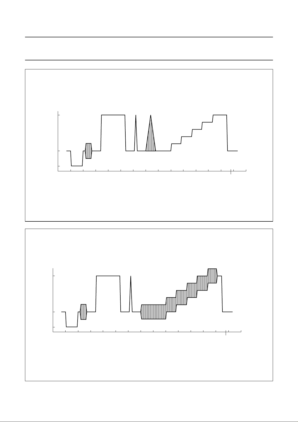
1. Ratio between the CCIR 17-line bar amplitude (corresponding to the level difference between black and white;
see Fig.4) and the RMS value of the noise on a black line (line 22 or 335) measured on the video signal after
demodulation. Measurement is done for frequencies between 200 kHz and 5 MHz. Measurement is unweighted.
2. Measured on CCIR 330 line, corresponding to a 5-step staircase with a chroma carrier of amplitude equal to 0.3
times the voltage between sync pulse and white (see Fig.5). The video signal is 500 mV (p-p). The modulation depth
is adjusted using the I2C-bus to MD setting = 4 (82.5% typical modulation depth).
3. Measured with a spectrum analyser with ‘peak hold’ function, applying a 500 mV (p-p) sine wave at the video input
of the IC, with a sweeping frequency between 0.5 and 6.0 MHz. The reference is the value measured at 1.0 MHz.
4. To have a deviation between 50 and 250 kHz, the audio frequency must be higher than 100 Hz.
5. Measured with an audio frequency of 1 kHz with a level adjusted to get a deviation of 50 kHz with DEV setting = 2,
using CCIR 468-3 weighting filter, with a quasi-peak detection. The input signal has pre-emphasis and the receiver
has de-emphasis. Video signal is 500 mV (p-p) EBU colour bars on pin VIDEO.
1997 Jan 08 16
Page 17

Philips Semiconductors Preliminary specification
Universal I2C-bus programmable RF
TDA8822
modulator
6. Measured with no pre-emphasis on the audio input and no de-emphasis in the receiver. Measurement is done for
frequencies between 50 Hz and 15 kHz, reference is the level measured at 1 kHz.
7. The accuracy only depends on the accuracy of the reference frequency (accuracy of the crystal). Notice that the
value of the capacitor in series with the crystal must be chosen to be as close as possible to the load capacitance of
the crystal.
8. Except for the harmonics of the RF oscillator frequency and for the combinations between the RF oscillator
frequency and the sound oscillator frequency (fRF+2fs, 2fRF+fs, etc.). This measurement includes the spurious at
the1⁄4fRF,1⁄2fRF and3⁄4f
9. Chroma beat
a) For PAL: measured applying a 4.43 MHz sine wave of 200 mV (p-p) at the video input. Measurement is the
difference between the level of the unmodulated picture carrier and the level of the spike appearing at the
frequency of the picture carrier plus 1.07 MHz for PAL B/G, 1.57 MHz for PAL I and 2.07 MHz for PAL D/K.
b) For NTSC: measured applying a 3.58 MHz sine wave of 200 mV (p-p) at the video input. Measurement is the
difference between the level of the unmodulated picture carrier and the level of the spike appearing at the
frequency of the picture carrier plus 920 kHz.
10. NICAM beat
a) For PAL B/G: measured applying a sine wave of 150 mV (p-p) at 5.85 MHz on the NICAM input. Measurement
is the difference between the level of the unmodulated picture carrier and the level of the spike appearing at the
frequency of the picture carrier plus 350 kHz or 5.15 MHz.
b) For PAL I: measured applying a sine wave of 150 mV (p-p) at 6.552 MHz on the NICAM input. Measurement is
the difference between the level of the unmodulated picture carrier and the level of the spike appearing at the
frequency of the picture carrier plus 552 kHz or 5.448 MHz.
11. NICAM eye height and Bit Error Rate measurement conditions:
a) A NICAM frame is applied from a Textronix 728E in B/G mode on the NICAM input of the TDA8822 through an
attenuator to get 150 mV (p-p). The sound subcarrier is set to 5.5 MHz (SC = 1) and the picture to sound ratio is
set to -12 dB (PS = 1). There is no video signal applied to the video input and no audio signal on the audio input.
b) The RF carrier is demodulated with a Rohde & Schwartz EMFP demodulator for PAL B/G, the sound trap filter is
set off, and the video signal is fed to a Textronix 728D NICAM demodulator for B/G. Measurements of the eye
height and bit error rate are done on the 728D.
RF.
1997 Jan 08 17
Page 18
Philips Semiconductors Preliminary specification
Universal I2C-bus programmable RF
modulator
handbook, full pagewidth
1 V
0.3 V
0 V
010203040 50 60
t (µs)
TDA8822
MBE396
64
70
handbook, full pagewidth
1 V
0.3 V
0 V
Fig.4 CCIR insertion line 17.
010203040 50 60
t (µs)
MBE397
64
70
Fig.5 CCIR insertion line 330.
1997 Jan 08 18
Page 19
Philips Semiconductors Preliminary specification
Universal I2C-bus programmable RF
modulator
INTERNAL PIN CONFIGURATION
handbook, full pagewidth
1
V
CCA
2
ACP
V
CCD
DGND
regulated voltage
PREEMPH
3
V
CCA
AGND
V
CCA
AGND
regulated voltage
VOLTAGE
REGULATOR
regulated
voltage
V
CCA
V
CCA
AGND
regulator voltage
AGND
V
CCA
AGND
TDA8822
24
VIDEO
23
AGND
22
AUDIO
21
NICAM
20
RFGND
19
RFA
18
RFB
RFOSCA
RFOSCB
OGND
RFOSCC
RFOSCD
VVT
VCP
V
CCD
XTAL
4
5
6
7
8
9
DGND
V
CCD
10
11
12
V
CCD
DGND
DGND
V
CCD
DGND
V
DGND
V
CCD
DGND
CCD
V
DGND
CCD
MGE681
17
TPSG
16
P0
15
SDA
14
SCL
13
DGND
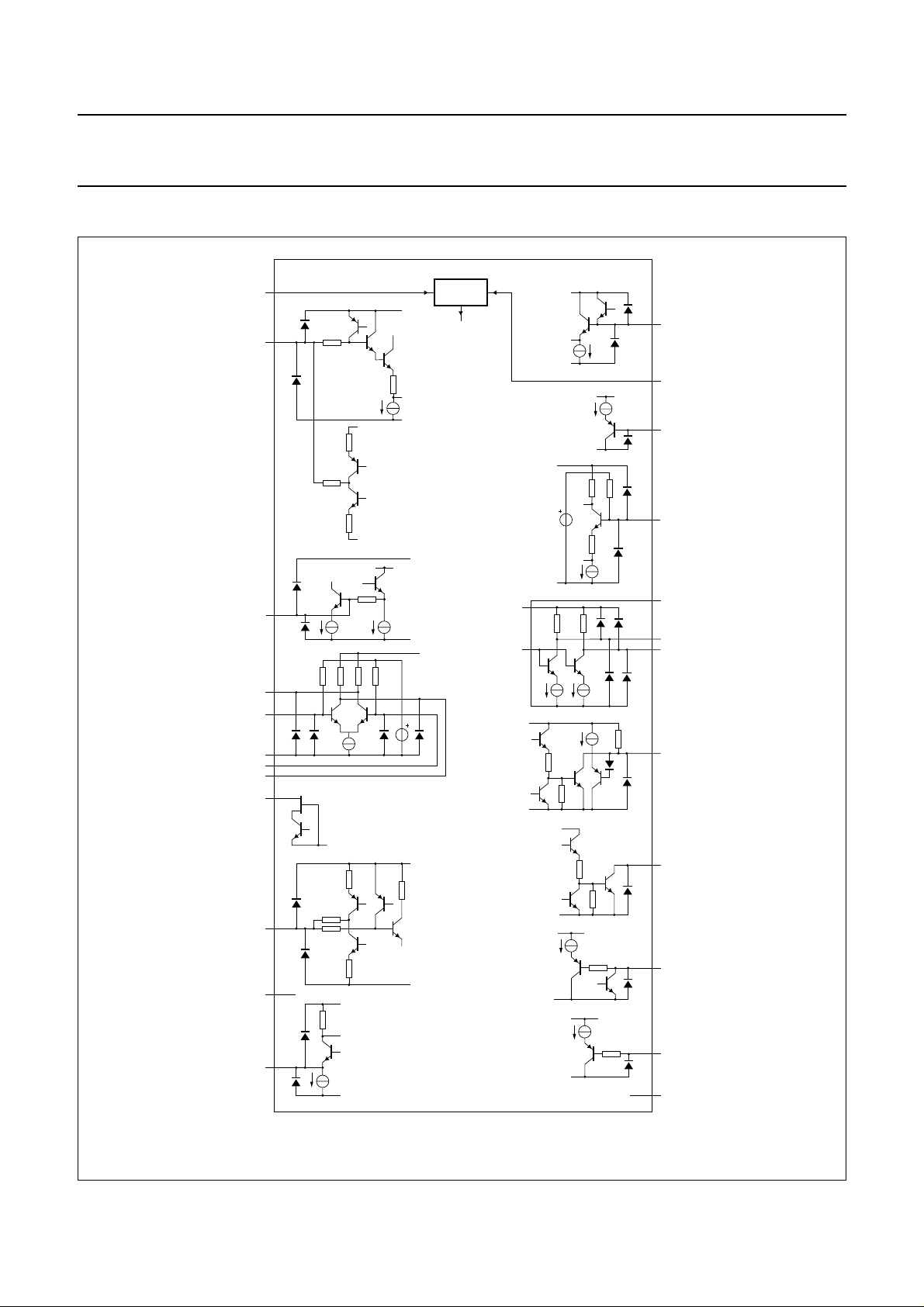
Fig.6 Pin equivalent circuit for each pin.
1997 Jan 08 19
Page 20
Philips Semiconductors Preliminary specification
Universal I2C-bus programmable RF
modulator
APPLICATION INFORMATION
SCL
SDA
NICAM
AUDIO
VIDEO
470 Ω
R26
82 Ω
R21
51 Ω
R24
C21
1 nF
100 nF
R25
470 Ω
C22
220 pF
R27
220 kΩ
C24
VIDEO23AGND22AUDIO21NICAM20RFGND19RFA18RFB17TPSG16P0
24
R22
12
kΩ
R14
270 Ω
handbook, full pagewidth
R15
270 Ω
C18
C19
100
100
pF
pF
R18
1 kΩ
TDA8822
RFB
RFA
P0
DGND
SCL
SDA
15
14
13
TDA8822
8
7
6
5
4
3
2
1
RFOSCD
OGND
(1)
RFOSCC
C7
(1)
C6
(1)
R7 R8
22 kΩ 15 kΩ
C9
10 nF
C8
(1)
V
= 5 V
CC
VVT = 33 V
C25
CCA
C1
100
nF
R2
4.7
kΩ
10
nF
C2
2.2
EMPH
µF
C26
68 nF
C4
(1)
C5
(1)
L1
(1)
D1
R5
22 kΩ
RFOSCB
RFOSCA
PRE
ACP
V
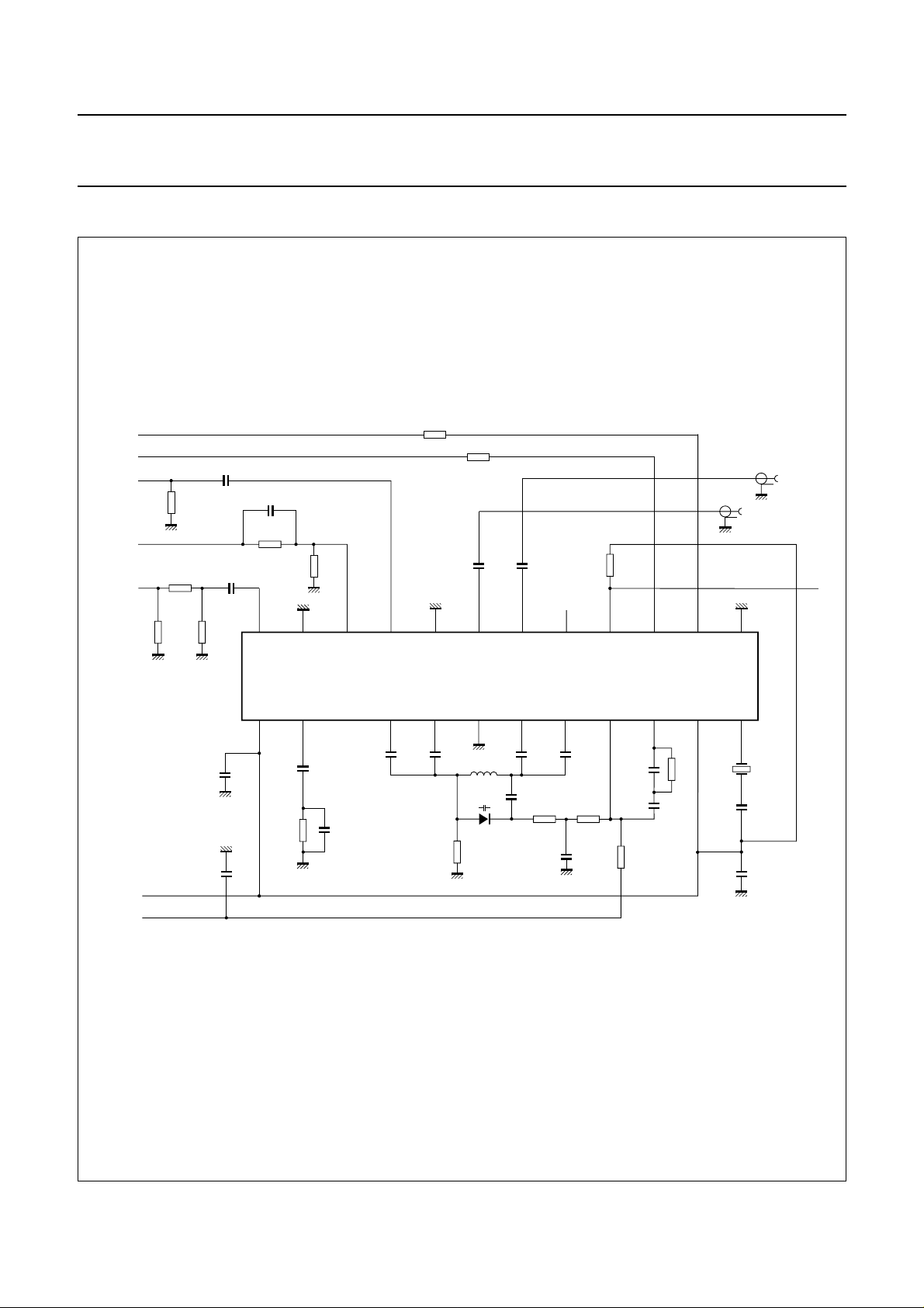
(1) The components marked: C4, C5, C6, C7, C8, L1 and D1 must be chosen from Table 11 to get the desired frequency range.
9
VVT
C10
4.7
nF
R9
27 kΩ
10
VCP
C27
100 nF
R10
33
kΩ
12
11
XTAL
V
CCD
XTAL1
4 MHz
C12
18 pF
C11
10 nF
MGE678
Fig.7 Reference application.
1997 Jan 08 20
Page 21

Philips Semiconductors Preliminary specification
Universal I2C-bus programmable RF
TDA8822
modulator
Application design
In the design of the application, it is highly recommended to separate the part of the RF oscillator as much as possible
from the part of the RF outputs in order to avoid parasitic coupling between these two parts.
A good solution is shielding the RF oscillator part to avoid radiation from and to this part. The pin OGND must be
connected to the shielding box and to ground.
The frequency range the IC covers is fixed by the choice of the components marked with a note (1) in Fig.7. For these
components, it is recommended to use the values indicated in Table 11.
Table 11 Components to be used for the RF oscillator
BAND
VHF1 47 to 130 MHz 5.6 pF 100pF BB132 14.5 3.0 mm 0.3 mm
VHF3 130 to 350 MHz 4.7 pF 150 pF BB133 4.5 3.0 mm 0.4 mm
UHF 470 to 860 MHz 1.8 pF 22 pF BB134 1.5 2.5 mm 0.5 mm
Video input (pin 24)
The video input level on the IC is of 500 mV (p-p). In most
of the cases, the available video signals are of 1 V (p-p)
with a source impedance of 75 Ω.
To handle this kind of signal, we use a resistive divider with
two 470 Ω resistors (R24 and R25 in Fig.7) to divide the
1 V (p-p) signal down to 500 mV (p-p). In order to get an
input impedance of 75 Ω, a resistor of 82 Ω is implemented
in parallel to the divider (R26 in Fig.7).
Audio pre-emphasis
The capacitor C22 connected in parallel with R27 is
defining the time constant for the pre-emphasis following
Table 12.
Table 12 Choice of the pre-emphasis constant
STANDARD
special; note 1 no capacitor −
Note
1. This mode has to be considered if the pre-emphasis is
applied else-where on the path of the audio signal, or
if there is no need for pre-emphasis in specific
applications. Note also that the pre-emphasis can be
done by connecting a capacitor between pin
PREEMPH (pin 3) and ground. The value for this
capacitor is 10 nF for PAL and 15 nF for NTSC.
FREQUENCY
RANGE
CAPACITOR
C22
NTSC 330 pF 75 µs
PAL 220 pF 50 µs
VALUE FOR
C4, C5, C7, C8
TIME
CONSTANT
VALUE
FOR C6
D1
Audio input (pin 22)
The IC is sensitive to 45 mV (p-p) on pin AUDIO and the
DC voltage on this pin is close to 0 V.
This pin needs to be grounded through a 12 kΩ resistor
(R22 in Fig.7). Care must then be taken if a coupling
capacitor needs to be implemented on the audio path to
connect it between the signal source and the input, with
the resistor of 12 kΩ still connected to the AUDIO pin.
NICAM input (pin 21)
The NICAM pin is sensitive to 150 mV (p-p) to reach a
level between picture carrier and NICAM carrier of typical
−20 dBc.
It is possible to put on this pin either a NICAM modulated
carrier for a NICAM application or a frequency modulated
carrier for the stereo system with a second FM carrier used
e.g. in Germany.
In a specific application where the main sound subcarrier
would be generated outside the IC, it is also possible to
inject the main sound carrier to this pin, with a level
depending on the wanted P/S. In this event, it is necessary
to stop the internal sound oscillator by setting RF0 to
logic 0 and TPSG to logic 1 (see Table 8).
L1: NUMBER
OF TURNS
L1:COIL
DIAMETER
L1: WIRE
DIAMETER
1997 Jan 08 21
Page 22

Philips Semiconductors Preliminary specification
Universal I2C-bus programmable RF
modulator
TPSG input/output (pin 17)
As already mentioned, this pin can be used either as an
input or as an output.
• As an input, it allows to turn on the TPSG, without
changing anything to the word the TDA8822 is
programmed through the I2C-bus.
In this mode, it is simply necessary to connect a switch
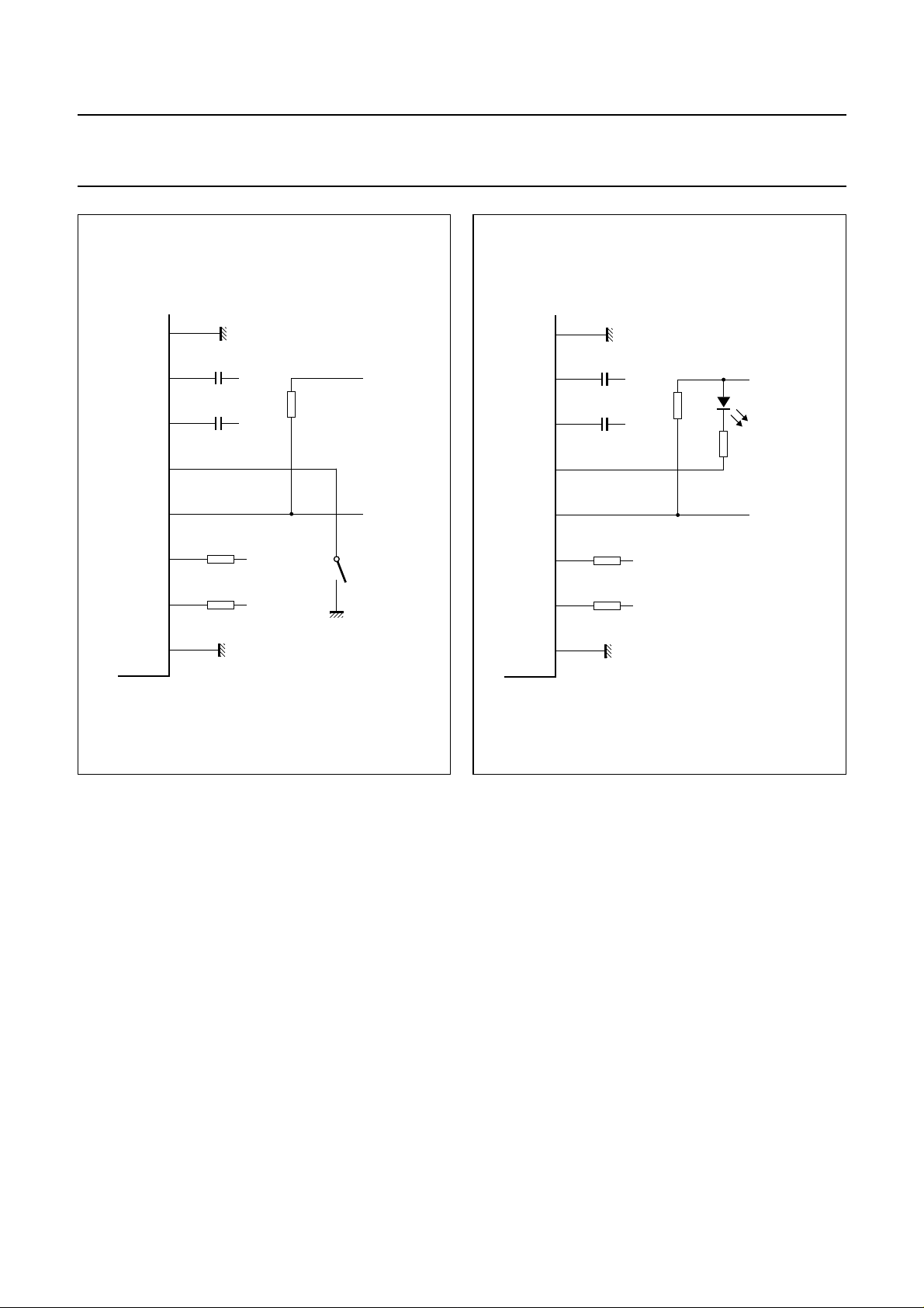
between the pin TPSG and DGND (see Fig.8). If the
switch is open, then the TPSG is selected
corresponding to the I2C-bus programming; if the switch
is closed, then the TPSG is on.
• As an output, it allows to indicate e.g. with an LED that
the TPSG has been programmed on using the I2C-bus.
In this mode, the pin acts as an open-collector output
port, it is possible to connect a LED to the 5 V power
supply with a series resistor to limit the current to about
10 mA (see Fig.9).
XTAL pin (pin 12)
This pin is connected to a 4 MHz crystal in series with a
capacitor. The value of this capacitor has to be as close as
possible to the load capacitance of the crystal.
It is also possible to drive the IC with an external 4 MHz
signal from a voltage source. A level of 50 mV(RMS)
insures stable operation. A capacitor of about 18 pF and a
resistor of 680 Ω needs to be placed in series with the
voltage source.
ACP pin (pin 2)
This pin is the charge pump output for the sound subcarrier
PLL as well as the input of the sound subcarrier VCO.
It is necessary to connect the loop filter between this pin
and ground. The loop filter indicated in Fig.7 gives a cut-off
frequency lower than 20 Hz.
TDA8822
If a cutoff frequency slightly higher than 20 Hz can be
accepted, it is possible to reduce the value of the 2.2 µF
capacitor (C2) to 220 nF. In this case C26 needs to be
changed from 68 nf to 22 nF and R3 needs to be changed
from 4.7 kΩ to 33 kΩ.
RF outputs (pins 18 and 19)
For inexpensive applications, it is possible to use the IC
with an asymmetrical output.
In an asymmetrical application, the unused output pin
must be loaded with a load as close as possible to the load
connected to the used pin.
A good improvement in performance is obtained using a
symmetrical to asymmetrical transformer
(balun; balance-to-unbalance) connected between the two
outputs. In this event both outputs have their loads
matched. The level of the RF second harmonic, and the
spurious outside channel is decreasing. The parasitic
coupling between RF outputs and RF oscillator is also
reduced.
RF harmonics
This IC has been designed to have the lowest level of
unwanted RF harmonics at the frequencies where these
are the hardest to be filtered out, especially for the second
harmonic of the RF carrier at the lowest frequencies of the
UHF band.
It is possible to reduce the level of the second harmonic by
using a wide-band transformer at the output of the IC and
create a symmetrical application.
To reduce the out-of-band harmonics and especially the
third one, it is necessary to use a low-pass filter at the
output of the IC.
1997 Jan 08 22
Page 23
Philips Semiconductors Preliminary specification
Universal I2C-bus programmable RF
modulator
handbook, halfpage
20
19
18
17
16
15
14
13
RFGND
RFA
RFB
TPSG
P0
SDA
SCL
DGND
C19
100 pF
C18
100 pF
R15
270 Ω
R14
270 Ω
RFA
RFB
SDA
SCL
R15
VCC = 5 V
1 kΩ
P0
S1
MGE679
handbook, halfpage
20
19
18
17
16
15
14
13
RFGND
RFA
RFB
TPSG
P0
SDA
SCL
DGND
C19
100 pF
C18
100 pF
R15
270 Ω
R14
270 Ω
RFA
RFB
SDA
SCL
R15
1 kΩ
R17
TDA8822
VCC = 5 V
330 Ω
P0
MGE680
Fig.8 Use of the pin TPSG as an input.
Fig.9 Use of the pin TPSG as an output.
1997 Jan 08 23
Page 24
Philips Semiconductors Preliminary specification
Universal I2C-bus programmable RF
modulator
PACKAGE OUTLINES
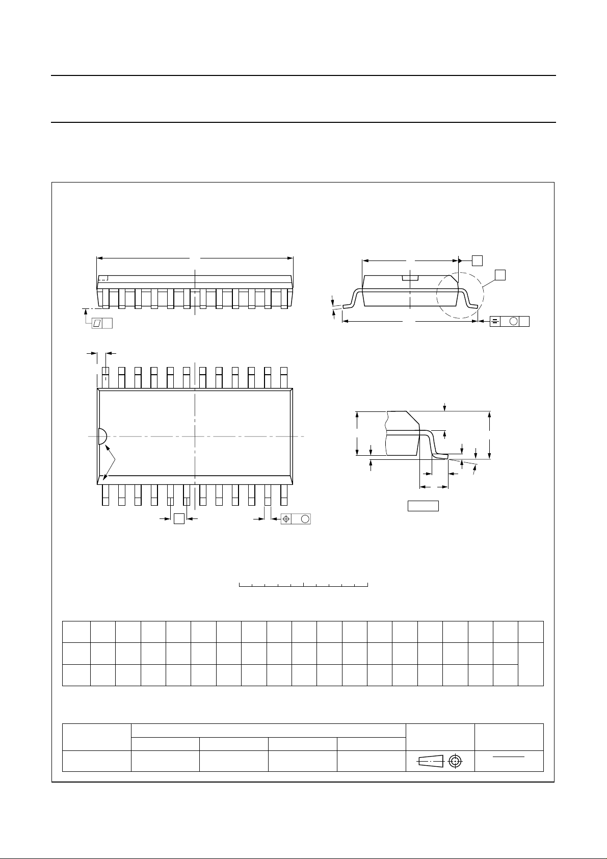
SO24: plastic small outline package; 24 leads; body width 7.5 mm
D
c
y
Z
24
13
TDA8822
SOT137-1
E
H
E
A
X
v M
A
pin 1 index
1
e
0 5 10 mm
DIMENSIONS (inch dimensions are derived from the original mm dimensions)
mm
A
max.
2.65
0.10
A1A2A
0.30
2.45
0.10
2.25
0.012
0.096
0.004
0.089
0.25
0.01
b
3
p
0.49
0.32
0.36
0.23
0.019
0.013
0.014
0.009
UNIT
inches
Note
1. Plastic or metal protrusions of 0.15 mm maximum per side are not included.
(1)E(1) (1)
cD
15.6
15.2
0.61
0.60
12
w M
b
p
scale
eHELLpQ
7.6
1.27
7.4
0.30
0.050
0.29
10.65
10.00
0.419
0.394
A
1.4
0.055
Q
2
A
1
detail X
1.1
1.1
0.4
0.043
0.016
1.0
0.043
0.039
0.25
0.01
L
p
L
(A )
0.25 0.1
0.01
A
3
θ
ywv θ
Z
0.9
0.4
0.035
0.004
0.016
o
8
o
0
OUTLINE
VERSION
SOT137-1
IEC JEDEC EIAJ
075E05 MS-013AD
REFERENCES
1997 Jan 08 24
EUROPEAN
PROJECTION
ISSUE DATE
95-01-24
97-05-22
Page 25
Philips Semiconductors Preliminary specification
Universal I2C-bus programmable RF
modulator
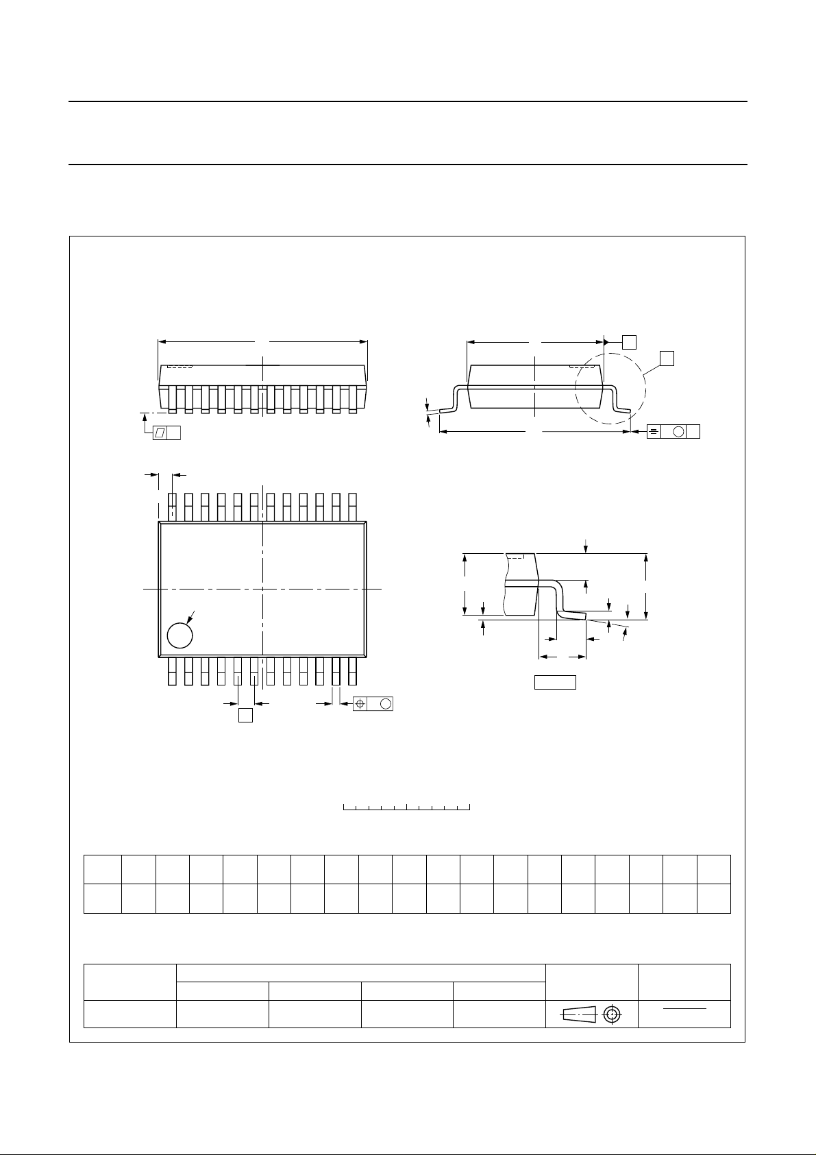
SSOP24: plastic shrink small outline package; 24 leads; body width 5.3 mm
D
c
y
Z
24 13
TDA8822
SOT340-1
E
H
E
A
X
v M
A
pin 1 index
112
w M
b
e
DIMENSIONS (mm are the original dimensions)
mm
A
max.
2.0
0.21
0.05
1.80
1.65
0.25
b
3
p
0.38
0.25
UNIT A1A2A
Note
1. Plastic or metal protrusions of 0.20 mm maximum per side are not included.
p
0 2.5 5 mm
(1)E(1) (1)
cD
0.20
8.4
0.09
8.0
scale
eHELLpQZywv θ
5.4
0.65 1.25
5.2
7.9
7.6
Q
A
2
A
1
detail X
1.03
0.9
0.63
0.7
(A )
L
p
L
A
3
θ
0.13 0.10.2
0.8
0.4
o
8
o
0
OUTLINE
VERSION
SOT340-1 MO-150AG
IEC JEDEC EIAJ
REFERENCES
1997 Jan 08 25
EUROPEAN
PROJECTION
ISSUE DATE
93-09-08
95-02-04
Page 26

Philips Semiconductors Preliminary specification
Universal I2C-bus programmable RF
modulator
SOLDERING
Introduction
There is no soldering method that is ideal for all IC
packages. Wave soldering is often preferred when
through-hole and surface mounted components are mixed
on one printed-circuit board. However, wave soldering is
not always suitable for surface mounted ICs, or for
printed-circuits with high population densities. In these
situations reflow soldering is often used.
This text gives a very brief insight to a complex technology.
A more in-depth account of soldering ICs can be found in
“IC Package Databook”
our
Reflow soldering
Reflow soldering techniques are suitable for all SO and
SSOP packages.
Reflow soldering requires solder paste (a suspension of
fine solder particles, flux and binding agent) to be applied
to the printed-circuit board by screen printing, stencilling or
pressure-syringe dispensing before package placement.
Several techniques exist for reflowing; for example,
thermal conduction by heated belt. Dwell times vary
between 50 and 300 seconds depending on heating
method. Typical reflow temperatures range from
215 to 250 °C.
Preheating is necessary to dry the paste and evaporate
the binding agent. Preheating duration: 45 minutes at
45 °C.
Wave soldering
(order code 9398 652 90011).
TDA8822
SSOP
Wave soldering is not recommended for SSOP packages.
This is because of the likelihood of solder bridging due to
closely-spaced leads and the possibility of incomplete
solder penetration in multi-lead devices.
If wave soldering cannot be avoided, the following
conditions must be observed:
• A double-wave (a turbulent wave with high upward
pressure followed by a smooth laminar wave)
soldering technique should be used.
• The longitudinal axis of the package footprint must
be parallel to the solder flow and must incorporate
solder thieves at the downstream end.
Even with these conditions, only consider wave
soldering SSOP packages that have a body width of
4.4 mm, that is SSOP16 (SOT369-1) or
SSOP20 (SOT266-1).
METHOD (SO AND SSOP)
During placement and before soldering, the package must
be fixed with a droplet of adhesive. The adhesive can be
applied by screen printing, pin transfer or syringe
dispensing. The package can be soldered after the
adhesive is cured.
Maximum permissible solder temperature is 260 °C, and
maximum duration of package immersion in solder is
10 seconds, if cooled to less than 150 °C within
6 seconds. Typical dwell time is 4 seconds at 250 °C.
A mildly-activated flux will eliminate the need for removal
of corrosive residues in most applications.
SO
Wave soldering techniques can be used for all SO
packages if the following conditions are observed:
• A double-wave (a turbulent wave with high upward
pressure followed by a smooth laminar wave) soldering
technique should be used.
• The longitudinal axis of the package footprint must be
parallel to the solder flow.
• The package footprint must incorporate solder thieves at
the downstream end.
1997 Jan 08 26
Repairing soldered joints
Fix the component by first soldering two diagonally-
opposite end leads. Use only a low voltage soldering iron
(less than 24 V) applied to the flat part of the lead. Contact
time must be limited to 10 seconds at up to 300 °C. When
using a dedicated tool, all other leads can be soldered in
one operation within 2 to 5 seconds between
270 and 320 °C.
Page 27

Philips Semiconductors Preliminary specification
Universal I2C-bus programmable RF
TDA8822
modulator
DEFINITIONS
Data sheet status
Objective specification This data sheet contains target or goal specifications for product development.
Preliminary specification This data sheet contains preliminary data; supplementary data may be published later.
Product specification This data sheet contains final product specifications.
Limiting values
Limiting values given are in accordance with the Absolute Maximum Rating System (IEC 134). Stress above one or
more of the limiting values may cause permanent damage to the device. These are stress ratings only and operation
of the device at these or at any other conditions above those given in the Characteristics sections of the specification
is not implied. Exposure to limiting values for extended periods may affect device reliability.
Application information
Where application information is given, it is advisory and does not form part of the specification.
LIFE SUPPORT APPLICATIONS
These products are not designed for use in life support appliances, devices, or systems where malfunction of these
products can reasonably be expected to result in personal injury. Philips customers using or selling these products for
use in such applications do so at their own risk and agree to fully indemnify Philips for any damages resulting from such
improper use or sale.
PURCHASE OF PHILIPS I
Purchase of Philips I
components in the I2C system provided the system conforms to the I2C specification defined by
Philips. This specification can be ordered using the code 9398 393 40011.
2
C COMPONENTS
2
C components conveys a license under the Philips’ I2C patent to use the
1997 Jan 08 27
Page 28

Philips Semiconductors – a worldwide company
Argentina: see South America
Australia: 34 Waterloo Road, NORTH RYDE, NSW 2113,
Tel. +61 2 9805 4455, Fax. +61 2 9805 4466
Austria: Computerstr. 6, A-1101 WIEN, P.O. Box 213,
Tel. +43 1 60 101, Fax. +43 1 60 101 1210
Belarus: Hotel Minsk Business Center, Bld. 3, r. 1211, Volodarski Str. 6,
220050 MINSK, Tel. +375 172 200 733, Fax. +375 172 200 773
Belgium: see The Netherlands
Brazil: see South America
Bulgaria: Philips Bulgaria Ltd., Energoproject, 15th floor,
51 James Bourchier Blvd., 1407 SOFIA,
Tel. +359 2 689 211, Fax. +359 2 689 102
Canada: PHILIPS SEMICONDUCTORS/COMPONENTS,
Tel. +1 800 234 7381
China/Hong Kong: 501 Hong Kong Industrial Technology Centre,
72 Tat Chee Avenue, Kowloon Tong, HONG KONG,
Tel. +852 2319 7888, Fax. +852 2319 7700
Colombia: see South America
Czech Republic: see Austria
Denmark: Prags Boulevard 80, PB 1919, DK-2300 COPENHAGEN S,
Tel. +45 32 88 2636, Fax. +45 31 57 1949
Finland: Sinikalliontie 3, FIN-02630 ESPOO,
Tel. +358 9 615800, Fax. +358 9 61580/xxx
France: 4 Rue du Port-aux-Vins, BP317, 92156 SURESNES Cedex,
Tel. +33 1 40 99 6161, Fax. +33 1 40 99 6427
Germany: Hammerbrookstraße 69, D-20097 HAMBURG,
Tel. +49 40 23 53 60, Fax. +49 40 23 536 300
Greece: No. 15, 25th March Street, GR 17778 TAVROS/ATHENS,
Tel. +30 1 4894 339/239, Fax. +30 1 4814 240
Hungary: see Austria
India: Philips INDIA Ltd, Shivsagar Estate, A Block, Dr. Annie Besant Rd.
Worli, MUMBAI 400 018, Tel. +91 22 4938 541, Fax. +91 22 4938 722
Indonesia: see Singapore
Ireland: Newstead, Clonskeagh, DUBLIN 14,
Tel. +353 1 7640 000, Fax. +353 1 7640 200
Israel: RAPAC Electronics, 7 Kehilat Saloniki St, TEL AVIV 61180,
Tel. +972 3 645 0444, Fax. +972 3 649 1007
Italy: PHILIPS SEMICONDUCTORS, Piazza IV Novembre 3,
20124 MILANO, Tel. +39 2 6752 2531, Fax. +39 2 6752 2557
Japan: Philips Bldg 13-37, Kohnan 2-chome, Minato-ku, TOKYO 108,
Tel. +81 3 3740 5130, Fax. +81 3 3740 5077
Korea: Philips House, 260-199 Itaewon-dong, Yongsan-ku, SEOUL,
Tel. +82 2 709 1412, Fax. +82 2 709 1415
Malaysia: No. 76 Jalan Universiti, 46200 PETALING JAYA, SELANGOR,
Tel. +60 3 750 5214, Fax. +60 3 757 4880
Mexico: 5900 Gateway East, Suite 200, EL PASO, TEXAS 79905,
Tel. +9-5 800 234 7381
Middle East: see Italy
Netherlands: Postbus 90050, 5600 PB EINDHOVEN, Bldg. VB,
Tel. +31 40 27 82785, Fax. +31 40 27 88399
New Zealand: 2 Wagener Place, C.P.O. Box 1041, AUCKLAND,
Tel. +64 9 849 4160, Fax. +64 9 849 7811
Norway: Box 1, Manglerud 0612, OSLO,
Tel. +47 22 74 8000, Fax. +47 22 74 8341
Philippines: Philips Semiconductors Philippines Inc.,
106 Valero St. Salcedo Village, P.O. Box 2108 MCC, MAKATI,
Metro MANILA, Tel. +63 2 816 6380, Fax. +63 2 817 3474
Poland: Ul. Lukiska 10, PL 04-123 WARSZAWA,
Tel. +48 22 612 2831, Fax. +48 22 612 2327
Portugal: see Spain
Romania: see Italy
Russia: Philips Russia, Ul. Usatcheva 35A, 119048 MOSCOW,
Tel. +7 095 755 6918, Fax. +7 095 755 6919
Singapore: Lorong 1, Toa Payoh, SINGAPORE 1231,
Tel. +65 350 2538, Fax. +65 251 6500
Slovakia: see Austria
Slovenia: see Italy
South Africa: S.A. PHILIPS Pty Ltd., 195-215 Main Road Martindale,
2092 JOHANNESBURG, P.O. Box 7430 Johannesburg 2000,
Tel. +27 11 470 5911, Fax. +27 11 470 5494
South America: Rua do Rocio 220, 5th floor, Suite 51,
04552-903 São Paulo, SÃO PAULO - SP, Brazil,
Tel. +55 11 821 2333, Fax. +55 11 829 1849
Spain: Balmes 22, 08007 BARCELONA,
Tel. +34 3 301 6312, Fax. +34 3 301 4107
Sweden: Kottbygatan 7, Akalla, S-16485 STOCKHOLM,
Tel. +46 8 632 2000, Fax. +46 8 632 2745
Switzerland: Allmendstrasse 140, CH-8027 ZÜRICH,
Tel. +41 1 488 2686, Fax. +41 1 481 7730
Taiwan: Philips Semiconductors, 6F, No. 96, Chien Kuo N. Rd., Sec. 1,
TAIPEI, Taiwan Tel. +886 2 2134 2870, Fax. +886 2 2134 2874
Thailand: PHILIPS ELECTRONICS (THAILAND) Ltd.,
209/2 Sanpavuth-Bangna Road Prakanong, BANGKOK 10260,
Tel. +66 2 745 4090, Fax. +66 2 398 0793
Turkey: Talatpasa Cad. No. 5, 80640 GÜLTEPE/ISTANBUL,
Tel. +90 212 279 2770, Fax. +90 212 282 6707
Ukraine: PHILIPS UKRAINE, 4 Patrice Lumumba str., Building B, Floor 7,
252042 KIEV, Tel. +380 44 264 2776, Fax. +380 44 268 0461
United Kingdom: Philips Semiconductors Ltd., 276 Bath Road, Hayes,
MIDDLESEX UB3 5BX, Tel. +44 181 730 5000, Fax. +44 181 754 8421
United States: 811 East Arques Avenue, SUNNYVALE, CA 94088-3409,
Tel. +1 800 234 7381
Uruguay: see South America
Vietnam: see Singapore
Yugoslavia: PHILIPS, Trg N. Pasica 5/v, 11000 BEOGRAD,
Tel. +381 11 625 344, Fax.+381 11 635 777
For all other countries apply to: Philips Semiconductors, Marketing & Sales Communications,
Building BE-p, P.O. Box 218, 5600 MD EINDHOVEN, The Netherlands, Fax. +31 40 27 24825
© Philips Electronics N.V. 1997 SCA53
All rights are reserved. Reproduction in whole or in part is prohibited without the prior written consent of the copyright owner.
The information presented in this document does not form part of any quotation or contract, is believed to be accurate and reliable and may be changed
without notice. No liability will be accepted by the publisher for any consequence of its use. Publication thereof does not convey nor imply any license
under patent- or other industrial or intellectual property rights.
Internet: http://www.semiconductors.philips.com
Printed in The Netherlands 537021/50/01/pp28 Date of release: 1997 Jan 08 Document order number: 9397 750 01601
 Loading...